

Abstract
Using a well-known galvanic displacement reaction, ∼25–40 μm long silver ribbons grown after mixing ∼50 nm copper particles with AgNO3 solution were observed as a function of Ag+ concentration and their growth was characterized in real-time and in situ by evanescent wave (EW) microscopy. At low Ag+ concentration, chain-like structures consisting of both Ag and Cu were observed. When the sequence of mixing these two reactants was reversed, different Ag microstructures (platelets and dendrites) were formed and were also characterized by EW microscopy. Dependence of the morphology of all these microstructures on silver ion concentration was determined by EW microscopy in conjunction with scanning and transmission electron microscopy.
Export citation and abstract BibTeX RIS
1. Introduction
A detailed understanding of dynamic processes like nucleation, growth and coalescence of nanoparticles and nanowires is of great interest across broad areas of nanotechnology, especially for the design and fabrication of nanostructures where it can help in optimizing the final microstructures. Real time imaging has proven to be an effective tool for investigating growth of nanoscale clusters [1–3], chemical dynamics in living cells [4], distribution of markers in migrating cells [5], cell view of life within 100 nm of the plasma membrane [6], dynamics of single-DNA molecules [7], etc. Electron microscopy [8–10], and optical imaging [11–13], are two of the most commonly used real time imaging techniques. For example, Evans et al [14], reported on the direct visualization of the growth of lead sulfide nanoparticle using in situ liquid transmission electron microscopy (TEM) where as Strelcov et al [15], reported on an in situ scanning electron microscopy (SEM) study of lithium intercalation in individual V2O5 nanowires. Stephan et al [16], showed that SEM imaging of biological samples (cells and tissues) can be performed under natural (hydrated) conditions but their method needed tedious sample preparation methods like special chamber design and staining.
Optical imaging remains in widespread use because of its versatility as a diagnostic and inspection tool due to its simplicity and ability to image samples in a fully hydrated condition. Some examples include the imaging of single silver (Ag) nanoparticles by dark-field optical microscopy [17], and observation of the growth of carbon nanotubes by remote microscope videography combined with pulsed laser irradiation [18].
Our very recent example of optical imaging was the use of in situ evanescent wave (EW) microscopy to visualize and characterize growth of Ag ribbons. EW measurements are based on total internal reflection (TIR) microscopy theory first introduced by Ambrose in 1961 to measure the movement of fibrocytes in tissue culture [19]. It was followed by McCutchen in 1964 who, using what he labeled as frustrated TIR, measured the surface topography of a large 4.4 mm glass ball and polyvinyl chloride surfaces [20]. Since then many advances have been made in TIR microscopy techniques, especially in confocal [6] and evanescent microscopy [21–23].
Our homebuilt experimental EW microscopy system is shown in figure 1 and is reproduced here from our earlier publication for ease of reference. EW microscopy uses the EW produced by the TIR of light at a glass–water interface. Under the condition of TIR, an EW is formed and propagates in the less dense medium along the interface with an intensity that decreases exponentially along the distance perpendicular to the glass–water interface (S-1). The EW wave can be used to illuminate a layer of material beyond the interface (the shaded area in figure 1) that may contain various structures within the penetration depth of the evanescent field. The scattered light can be imaged to characterize these structures. Due to the exponential drop in the intensity of the EW wave, the image intensity is very sensitive to movement of any object vertical to the same interface. The images appear bright when the objects of interest approach the interface and dim when they retreat in a way that is directly related to the EW field intensity. Also, only those objects that are present in the limited evanescent field penetration depth can be imaged or tracked by this technique [24]. Interestingly, it was suggested that this technique could be used to measure surface diffusion, molecular conformation of adsorbates, and cell development during cell culture, visualization of cell structures and dynamics etc [25].
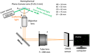
Figure 1. Diagram of our home built EW microscopy system (reproduced from [1] with permission from the Royal Society of Chemistry).
Download figure:
Standard image High-resolution imageHere, we report the results from our in situ and real time investigation of the details of the growth rates and morphology of anisotropic silver microstructures. These were created by the well-known galvanic displacement reaction between Cu particles and Ag+ ions (figure 2), carried out without a template in the absence of any external reducing agents or electric current. Also, the samples collected after several minutes of the in situ growth processes were analyzed by electron microscopy (SEM and TEM) to understand better the role of various parameters involved.
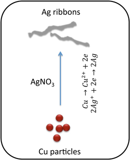
Figure 2. Schematic of Cu/Ag galvanic displacement reaction. (The drawing is not to scale.)
Download figure:
Standard image High-resolution imageIt is important to mention that there are several inherent limitations on the resolution that can be achieved by EW imaging. The resolution of the EW images is limited by the low magnification objective lens (50x) and is inherent to this method since using a higher numerical aperture and magnification lens limits ability to focus better. The image quality is also constrained by the very small (∼100 nm) EW field penetration depth. The associated slight defocusing leads to the appearance of fringes in EW images and it seems these cannot be completely eliminated. However, as our results show, that it is still possible to combine the real time in situ EW imaging with conventional SEM and TEM analysis to obtain an improved understanding of the processes involved in the growth of different microstructures of Ag.
2. Experimental details
2.1. Instrumental setup
In our experiments, a laser diode (532 and 15 mW) was used to illuminate a small amount of liquid containing the reactants placed on a hydrophobic antireflective film-coated hemispherical plano-convex lens (LA1951-A, THORLABS, USA; focal length = 25.3 mm; coating thickness = 350–700 nm, contact angle = 76°) (figure 1). The scattered light from the particles (labeled green in S-1(a)) and other structures that are in the evanescent field (the shaded area in figure 1) is collected by an area sensor of a CMOS digital camera (Baumer HXC20, pixel size 5.5 μm2) with an objective lens (numerical aperture: 0.45) and an infinity-corrected tube lens (focal length: 200 mm) and imaged. The videos and images were recorded by Silicon Software (GmbH micro Display 5.2.2) using a desktop computer.
2.2. Growth of anisotropic silver microstructures
Silver nitrate and copper powder (average particle size 50 nm) used in our experiments were purchased from Sigma-Aldrich, USA and used without any modification. Silver ribbons were grown by placing 40 μl of an aqueous dispersion (particle loadings of either 0.1 and 0.01 wt%) of the nominally 50 nm Cu nanoparticles in deionized water (18 Ω cm) onto the flat surface of the hemispherical glass lens followed by the addition of 60 μl AgNO3 solution with different values (0.2, 0.1, 0.05, 0.01, 0.005 and 0.001 M) of Ag ion concentration or [Ag+]. We also investigated the same galvanic reaction by first placing 60 μl AgNO3 solution on the glass lens followed by the addition of a drop (40 μl) of the Cu dispersion, i.e. the reverse of the above sequence. The results were quite different as discussed later.
2.3. SEM and TEM imaging
For SEM characterization, a drop of the liquid sample was placed on an aluminum stub dried at 60 °C for 5 min and examined using a high-resolution field emission SEM (JEOL7400) equipped with an energy-dispersive x-ray spectrometer. Samples prepared for TEM analysis by placing a drop of the solution on a carbon-coated copper grid and drying in air were imaged using a JEOL JEM-2010 operated at an accelerating voltage of 200 kV. Images were analyzed using Gatan Digital Micrograph Version 3.11.1.
3. Results and discussion
3.1. Ag ribbon growth
EW microscopy allows us to image continuously the growing ribbons in situ and in real-time using the same camera and software. One such video captured over 5.4 s at 100 frames s−1 is available in the supporting information (S-4). Longer videos can also be obtained but require considerable computer memory. In addition to the short time videos, the growth processes were monitored for several minutes and a large number of static images were captured at different time intervals and analyzed.
Figure 3 shows three sets of sequential images of different silver ribbons grown in the first set of experiments, i.e. when AgNO3 solution with three different [Ag+] was added to the Cu particle dispersion at a fixed Cu particle concentration (0.1 wt%). The fringes that appear in the EW images are most likely caused by slightly defocused imaging as reported by several authors [26, 27], or due to the Airy disk diffraction pattern [28], and it appears that these fringes cannot be eliminated completely.
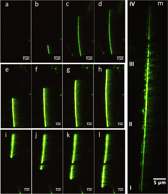
Figure 3. Sequential images with increasing time (see text for details) of three different silver ribbons grown at [Ag+] 0.2 M (a)–(d), 0.1 M (e)–(h) and 0.05 M (i)–(l) (the growth rate of these ribbons decreased with [Ag+]). Image in ('m') is one of the longest ribbons (∼74 μm) seen in our experiment ([Ag+] = 0.2 M) and it required ∼40 s to reach this length. All these ribbons were grown from a starting Cu particle concentration of 0.1 wt%.
Download figure:
Standard image High-resolution imageFigures 3(a)–(d) show the sequential images of a silver ribbon captured at 5 s intervals at [Ag+] of 0.2 M, figures 3(e)–(h) also captured at 5 s intervals but at a [Ag+] of 0.1 M, and finally figures 3(i)–(l) at [Ag+] of 0.05 M but at time intervals of 9, 8 and 6 s. It was observed that the induction time for ribbon formation varied based on Cu/[Ag+] ratio. Lower [Ag+] required a higher induction time for ribbon formation (see table 1).
Table 1. Induction time and growth rate with Ag+ concentration.
| [Ag+] (M) | Induction time (s) | Growth rate (μm s−1) |
|---|---|---|
| 0.2 | 7 ± 2 | ∼2.8 |
| 0.1 | 12 ± 2 | ∼1.2 |
| 0.05 | 17 ± 2 | ∼0.7 |
The ribbon growth rate calculated from the images in (b) and (c) is ∼2.8 μm s−1, from (e) to (f) is ∼1.2 μm s−1, and from (j) to (k) is ∼0.7 μm s−1, i.e., the rate decreases with decreasing [Ag+]. The intensities of the images of these ribbons are different, presumably because, as suggested earlier, they are located at different vertical distances from the glass–water interface. The average size of the Ag ribbons observed in our EW microscopy is 25–40 μm long (see S-2). There were several that were considerably longer and figure 3(m) shows one of the longest Ag ribbons (74 μm, ∼40 s growth time) observed in our experiments. It was grown at 0.2 M [Ag+]. It must have stayed almost but not quite parallel to the glass–water interface during its entire growth since the intensity along its length is not constant. Section II and III of this ribbon in figure 3(m) appears brighter compared to the other two sections (I and II and III and IV), indicating that this part of the ribbon was closer to the interface.
We also see a break in the Ag ribbons in some cases. For example, two segments with almost perfect alignment can be observed in figures 3(j)–(l). These must have originated from two directly opposite sides of the same Cu particle since it is difficult to imagine such a near perfect alignment if they originated from two different random Cu particles. In any case, this near perfect alignment is striking and dramatic and was also reported in our earlier publication.
3.2. Chain-like structures
As the [Ag+] was decreased further to 0.01 M, the images (figures 4(a)–(d)) obtained are quite different from those obtained above at the three higher [Ag+]. The structures in these images (a)–(d), which were obtained at 40 s time intervals, required considerably larger times to grow. Thus the structure/cluster formation in this case was delayed beyond about 80 s since the first semblance of a ribbon appeared only in figure 4(c) taken after 80 s compared to about 7–17 s (table 1) for the three higher concentrations.
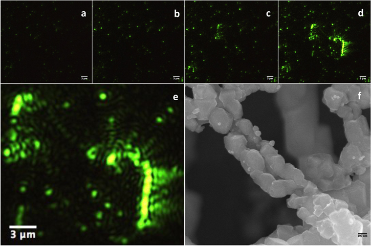
Figure 4. (a)–(d) Early stages of Ag ribbon formation observed at a low [Ag+] of 0.01 M recorded at 40 s intervals, (e) a magnified image of a portion of (d) and (f) high magnification SEM image of a chain like structure. This SEM image is from the same sample collected several minutes after the reactants were initially mixed. Starting Cu particle concentration in all these experiments is 0.1 wt%.
Download figure:
Standard image High-resolution imageFigure 4(d) shows what appear to be a large number of discrete clusters of different sizes. With time, the number of such clusters appearing in the evanescent field increased along with their size, with some of them eventually coalescing into 'chains', reaching ∼6 μm long, as can be seen in figures 4(d) and (e).
We call these chains, and not ribbon, since they appear to be morphologically very different from the Ag ribbons reported above in figure 3 and in our earlier publication [1] for the higher [Ag+]. For instance, the particular structure shown in figure 4(e) appears to consist of bright discrete segments connected by less intense links and this morphology is evident in the SEM images (compare S-5(c) and figure 4(f)). Such images are the reason we labeled them 'chains.' It is quite likely that these morphologies are a result of the scarcity of Ag ions around the growing structure leaving less intense Cu particle links, as discuss later. Interestingly, self-organized formation of chain-like structures consisting of only Ag by a solvothermal process from AgNO3 solutions were reported earlier [29, 30].
As discussed earlier, the EW images in 4(a)–(e) are not well resolved due to the low magnification objective lens (50X) and the low resolution is inherent to this method. In contrast, while the SEM image shown in 4(f) does not suffer from these limitations, it is not real time or in situ.
From the SEM image (figure 5(a)) of a sample consisting of structures grown under the same conditions as in figures 4(d) and (e), it appears that ribbons (top left corner in this image) and chains coexist, though the chain-like configurations seem to be predominant. If we lower [Ag+] further from 0.01 M to 0.005 M to 0.001 M, only the chain-like arrangement was observed at 0.005 M (figure 5(b)), but not at 0.001 M where individual clusters, some of them rod like, of different sizes appear (figure 5(c)) with most of them remaining discrete. The shortage of Ag ions required for continued growth must be significant under these conditions. Indeed, the EDX data shown in figure 5(d) of a small portion of a chain formed at 0.01 M and of a cluster formed at 0.001 M [Ag+] suggest that these structures consist of both Cu and Ag. The presence of Cu is a clear indication that not enough Ag+ are available to consume all of the Cu (see S-7, for the EDX spectrum of a Ag ribbon formed at a higher Ag+ concentration showing no Cu remaining). The Al peak in the EDX spectra is from the aluminum substrate used to mount the samples.
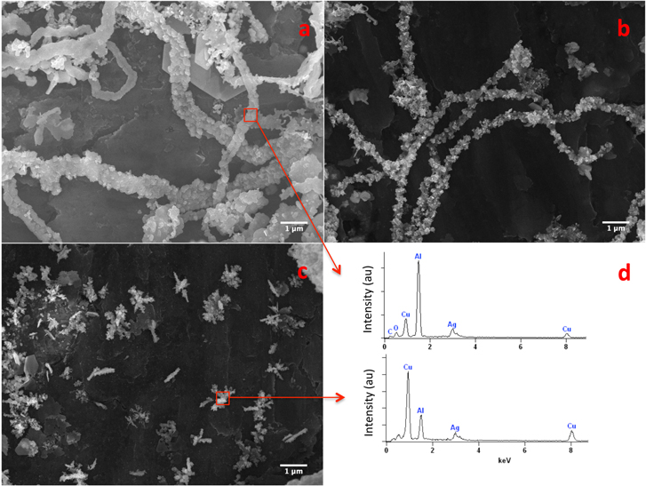
Figure 5. SEM images observed at three different [Ag+]: (a) 0.01 M, (b) 0.005 M (c) 0.001 M and (d) EDX spectrum of a small area of the images in ('a') and ('c').
Download figure:
Standard image High-resolution image3.3. Reverse addition of the reactants
When a second set of experiments in which the sequence of addition of Cu particles and Ag ions was reversed, dramatically different silver nanostructures were observed. Similar results were reported by other investigators [31], who grew different silver nano/micro structures by controlling reaction kinetics only. For example, Gu et al [32], reported the fabrication of silver dendrites on a copper substrate, which is similar to our second set of experiments. Also, Liu et al [33], reported obtaining various silver structures, including dendrites, flowers and spherical aggregates, just by controlling reaction kinetics in the presence of the amino acids glycine and leucine while Zhou et al [34], reported kinetically controlled growth of fine Au nanofractals through galvanic replacement reaction.
Figures 6(a) and (b) show the two EW images of radically different Ag nanostructures formed when 0.01 M AgNO3 was added to 0.01 wt% and 0.1 wt% Cu dispersions, respectively. Figures 6(c) and (d) (inserts show magnified images of a small portion in each image) show the SEM images of the above two samples taken after several minutes of the initial mixing of the reactants and may be compared with the images in figures 3(m), 4(f) and 5. At the lower Cu particle concentration, different sized platelets of Ag particles are formed (insert 6(c)) while with 0.1 wt% Cu, dendritic Ag nanostructures, reported and discussed by many investigators earlier [35–38], were obtained. The selected area EDX data confirm that, in both cases, these microstructures contain only Ag and suggest that all the Cu that must have been present in these structures during growth is consumed.
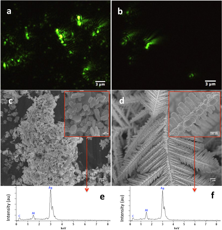
Figure 6. (a) and (b) EW images of Ag nanostructures obtained when Cu particles were added to silver nitrate solution at two different Cu/Ag ratios of Ag (0.01 M)/Cu (0.01 wt%) and Ag (0.01 M)/Cu (0.1 wt%), respectively; (c) and (d) show the corresponding SEM images obtained after several minutes of the same samples. Insets show magnified images of a small portion of the respective images whereas (e) and (f) represent the corresponding EDX spectra and shown the presence of only Ag and no Cu.
Download figure:
Standard image High-resolution image3.4. Proposed growth mechanism
These experiments, in which the addition process was reversed from the first set above, clearly indicate that this galvanic displacement and nanostructure formation process are kinetically controlled. The localized concentration of Ag ions must be playing an important role in determining the type of Ag nanostructure formed. For the same Cu to Ag atomic ratio, two different nanostructures (figures 5(a) and 6(b)) were observed just by changing the sequence of addition of these two precursors.
While several theories have been proposed to describe the growth of different Ag nano/microsturctures, there is no consensus. Here we propose a possible growth mechanism, demonstrated pictorially in figure 7, which can account for these variations in structure. It is based on the analysis of our real-time images captured by EW microscopy at the very early stages of ribbon formation as well as the large number of electron microscopy images. The induction times and growth pattern obtained from our real time in situ EW imaging has to become an essential part of the proposed silver microstructure formation and growth mechanism.
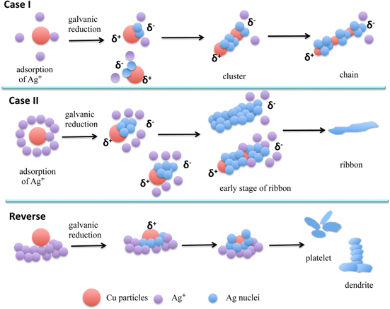
Figure 7. Schematic representation of the formation of chain, ribbon and other anisotropic Ag nanostructures at various experimental conditions. Case I: [Ag+] is low; case II: [Ag+] is relatively high, and reverse: Cu particles added to silver nitrate solution, which is the reverse of the sequence used in cases I and II. (The drawings are not to scale).
Download figure:
Standard image High-resolution imageThe Ag nano/microstructure formation process is illustrated in two different scenarios based on the addition sequence: first when Ag+ is added to Cu particles and second when the reverse is the case. In the first scenario, we have two cases, case-I when [Ag+] is low and case-II when [Ag+] is high. At the very beginning, Ag+ will adsorb on the Cu particle surface, which is followed by galvanic reduction during which a nano-electrode is created, current flowing from a local cathodic site to an anodic site [39]. As a result, Ag atoms are deposited on the cathodic site of the Cu surface and simultaneously anodic oxidation occurs by dissolution of the surface Cu atoms. This stage of the growth process cannot be resolved by our EW imaging technique and is manifest as the observed induction times.
Once the Ag deposition begins, the galvanic reaction continues as usual with the Ag ions still in solution, but in the vicinity of the Cu surface, capturing electrons from the Cu and deposited. The Ag particle adhering to the Cu surface have higher electronegativity than Cu and strongly attract electrons from Cu [39], causing the Cu particle to become positively charged, indicated by δ+ in figure 7. The electronegative Ag particles on the Cu particle surface have strong catalytic activity for the cathodic reaction and could provide a catalytic surface for the cathodic reaction (reduction of Ag ions) [39]. Therefore, the subsequent reduction process of Ag+ would be greatly enhanced, causing the Ag+ approaching the Cu surface to be reduced preferentially on the Ag particle sites rather than the on the bare Cu surface. At the same time agglomeration of Cu particles is also possible where another positively charged Cu surface will approach the anodic (negatively charged Ag particle) site of a Cu/Ag interface (figure 7 case-I, cluster). When there are not enough Ag atoms to consume the Cu particles in the structures, a chain like structure results eventually. Thus, the attachment of the δ+ surface of a Cu particle with the δ− surface (from the newly formed Ag particles) of a different Cu particle is crucial and presumably rate controlling in this process.
For higher Ag+ concentrations (case-II) we are most likely to observe the formation of continuous Ag ribbons (S-5(b) and (c)) since there is adequate supply of Ag+ to cover the entire surface of Cu particles, minimizing the possibility of their agglomeration. Thus the growth process in this case is driven by the larger Ag+ concentration all around the reacting surface of the Cu particle, leading to the formation of ribbons of Ag atoms without the intermittent Cu particles.
In the case of the second scenario of reverse addition (bottom row in figure 7), as the Cu particles are added, they are immediately surrounded by the Ag+ in solution leading to a relatively high concentration of Ag+ near the reacting Cu surface. If it is high enough to consume the entire particle, we observe Ag platelets or dendrites as illustrated in the bottom panel of figure 7. Thus it appears that the Ag nano/micro-structures formed depend on the rate of Ag+ reduction and the dissolution rate of Cu. Since the formation of these types of microstructures has been reported and discuss by many investigators earlier [35–38], we do not discuss this further here.
3.5. TEM data
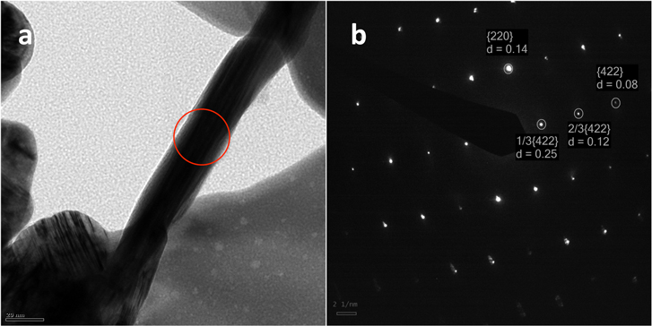
The TEM and selected area electron diffraction images (SAED) of one particular nanostructure of silver grown when 0.01 M Ag+ was added to 0.1 wt% Cu dispersion are shown in figures 8(a) and (b), respectively. The crystal plane indices associated with this are identified in the SAED pattern in figure 8(b). The set with a lattice spacing of 0.14 nm could be indexed to the {220} reflections of fcc silver, the intense spots in the [111] zone axis are allowed {220} Bragg reflections corresponding to the lattice spacing of 0.14 nm. The additional relatively weak spots in the diffraction pattern correspond to the normally forbidden 1/3 {422} and 2/3{422} Bragg reflections with lattice spacing of 0.25 nm and 0.12 nm, respectively. The outer set with a lattice spacing of 0.08 nm corresponds to the {422} reflection. All these data are consistent with the data reported earlier [1, 35].
Figure 8. (a) and (b) TEM and SAED image of a Ag microstructure. The lattice planes and spacings are identified in the image.
Download figure:
Standard image High-resolution image
The (111) stacking fault is responsible for the occurrence of the 1/3{422} forbidden reflection (forbidden for perfect fcc structures) and has indeed been observed when the flat top surface of nano/micro structures of Ag and Au is parallel to the (111) plane of their fcc crystal structures [40–42].
4. Conclusions
Using simple, cost-effective and straightforward real time and in situ EW microscopy, we were able to image and characterize the growth and evolution of different morphologies of Ag microstructures grown by the galvanic displacement reaction between Cu and Ag ions. The ratio of the Cu and Ag+ concentrations influenced the type of Ag structures—ribbon or chain-like—formed and these were imaged. It was observed that the growth rate of the ribbons drops with decreasing [Ag+]. We also found that the sequence of addition of the precursors changed the morphology from ribbons to clusters to platelets and dendrites. A possible process sequence for the galvanic reactions that can lead to the observed multiple morphologies is presented. These real time observations and data analysis can assist in minimizing the number of sequential imaging steps required by electron microscopy to characterize the growth of different Ag, Au and perhaps other microstructures.
Acknowledgments
This work was partly supported by the National Science Foundation, USA, through the I/U-CRC Metamaterials Award #1068040. We acknowledge Christopher Plunkett for help with equipment setup.