
Abstract
In this study we propose the use of a blend, comprising poly(3,4-ethylenedioxythiophene):polystyrene sulfonate (PEDOT:PSS) and polyvinyl alcohol (PVA), to be used as flexible, semitransparent and highly conductive material for electronic and optoelectronic devices. The electrical conductivity and optical transmittance of spray-deposited films of the blend, in different thicknesses and at different weight ratios, were studied in order to determine the most appropriate composition for optimal device performance and cost. We propose a direct method to determine the most appropriate blend composition to produce polymeric films with a desired sheet resistance, optical transmittance and cost, by using a diagram which considers the influence of blend composition and film thickness in a light-transmittance versus sheet resistance plot, mediated by the material cost per unit area. In this way, the present study establishes an empirical method to determine the PEDOT:PSS/PVA blend composition to be used as electrode material in optoelectronic devices which satisfies the desired conditions of optical transmittance, sheet resistance and cost-effectiveness.
Export citation and abstract BibTeX RIS
1. Introduction
Semiconducting polymers represent a class of electronic materials which have been applied in the development of a large variety of new electronic and optoelectronic devices, including organic light emitting diodes (OLEDs) [1–3], organic photovoltaic cells (OPVs) [4–7], organic field effect transistors (OFETs) [8], transducers for chemical or biochemical analysis [9, 10] and many other applications [11, 12]. Depending on the device functionality, a different semiconducting property of the active material is more relevant: charge-carrier recombination efficiency for OLEDs, energy conversion efficiency for OPVs and charge-carrier mobility for OFETs, for example. Concerning material processing, semiconducting polymers are also particularly interesting due to the solubility in most of organic solvents, allowing film deposition by relatively simple techniques like spin-coating, drop-casting, dip-coating [13], ink-jet printing [14], spray-coating [15, 16], stamp printing [17] and roll-to-roll printing [18].
In a similar fashion to their inorganic counterparts, the electrical conductivity of organic semiconductors can also vary by several orders of magnitude, spanning from almost insulating up to highly conductive materials. In the particular case of the latter, innumerous applications can be listed exploiting the unmatched combination of outstanding properties such as high electrical conductivity, ease of processing, flexibility, large-area covering and ultra-thin film formation, which are inherent to conducting polymers. For many of these applications, the most pertinent properties are the high electrical conductivity and the high optical transmittance in the visible range of the electromagnetic spectrum. However, other material properties like flexibility, film formation, chemical stability and wettability can also play an important role on the choice of the material or the composition to be used. Additionally, for commercial purposes, easy processing and low production cost (material cost and/or processing costs) also need to be well evaluated and considered.
To date, most of the applications of organic/polymeric optoelectronic devices have one of the electrodes made of an inorganic material: indium-tin oxide (ITO) [19–22], which is a highly conductive and highly transparent semiconducting material. In spite of its high conductivity and optical transmittance, ITO has few disadvantages that must be pointed out: relatively sophisticated deposition methods (RF-sputtering [23], pulse-laser deposition [24], etc), relatively high production cost, restricted flexibility and slight incompatibility with organic layers [25]. Recently, thin layers of semitransparent and highly conductive polymers have been considered [26–29] to replace ITO as transparent (or semitransparent) electrode for organic optoelectronic devices. The most promising material for this application is the poly(3,4-ethylenedioxythiophene):polystyrene sulfonate (PEDOT:PSS), a polymer mixture of a semiconducting polymer and an ionomer, which was initially used as hole injection layer in OLEDs due to the better alignment between the HOMO level of most of semiconducting polymers and the Fermi level of ITO. The development of new formulations of PEDOT:PSS, however, allowed the obtainment of thin polymeric films with conductivity values up to 103 S cm−1, suitable for application as electrode material, discarding the need of ITO. Additionally PEDOT:PSS is an incredibly versatile electroactive polymer which can be employed in a great variety of applications: deformation sensors [30], electro-active actuators [31, 32], thermistors [33], electrodes in piezoelectric sensors [34], fully polymeric microelectromechanical systems (MEMS) [35], active material for super-capacitors and super-batteries [36], rewritable memories [37] and semitransparent electrode/hole transport layer in optoelectronic devices such as organic light-emitting devices [26, 27] and OPVs [28, 38].
The properties of thin films based on PEDOT:PSS can be improved and controlled by using mixtures with other polymers like polyethylene oxide (PEO) [39], polyvinylidene difloride (PVDF) [39], polyethylene glycol methacrylate (PGMA) [39] and polyvinyl alcohol (PVA). PEDOT:PSS/PVA blends have been extensively studied, presenting many applications [40–44], including optrode-neural tissue interfaces [40], ultrahigh-strain sensors with controlled conductivity [41] and cloth sensing devices [42]. For these applications, one required property for the active material is a high mechanical fracture strain. It has been reported [43] that PEDOT:PSS/PVA blends, with a PEDOT:PSS content lower than 40%, exhibit about 90% of mechanical elongation break, which is quite close to the value obtained for pure PVA (111%). Additionally, it was observed that PEDOT:PSS/PVA solutions exhibit better wettability than pure PEDOT:PSS solutions onto glass substrates [44], which is a desirable characteristic for good film formation. Given that PEDOT:PSS is water-soluble, it is suitable for a wide variety of solution processing techniques, including large scale continuous processes like roll-to-roll [45], ink-jet printing [46] and large area spray-coating [47], resulting in low production costs. However, highly conductive PEDOT:PSS is still a relatively expensive material and it is not completely transparent in visible spectrum. In order to circumvent these undesired features and preserve the high electrical conductivity and processability needed for industrial scale printing processes [48] and transparent electronics [49], we propose the use of polymeric blends of PEDOT:PSS and polyvinyl alcohol (PVA), which is a water-soluble, low-cost and highly transparent polymer. To perform this study, we have used thin films of PEDOT:PSS/PVA, prepared by spray deposition [50], using different weight ratios between the blend components, to determine the most appropriate composition which results in optimal combination of optical transmittance, sheet resistance and cost.
2. Materials and methods
2.1. Materials
The conductive material used in all experiments was a PEDOT:PSS water dispersion commercialized as Clevios™ PH 1000, purchased from Heraeus. This material is a highly conductive polymer mixture dispersion which can give rise to polymeric films exhibiting electrical conductivity of up to 1000 S cm−1 when 5% (volume) of dimethyl sulfoxide (DMSO) or ethylene glycol [51] is previously added to the solution and post-baked after film deposition at 130 °C (403 K) for 15 min. The other blend component, polyvinyl alcohol (PVA), which is a highly transparent, water-soluble and low-cost polymer was obtained from Sigma-Aldrich (Mw 89 000–98 000, 99% hydrolyzed) and used in its present condition.
2.2. Sample preparation
PVA solutions were prepared by dissolving the polymer into purified water at 30 mg ml−1 (same concentration of the PEDOT:PSS solution) and stirring for 4 h at 90 °C (363 K). After complete dissolution of PVA, the PEDOT:PSS dispersion, with 5% (volume) of ethylene glycol as additive, was added in the desired weight ratio and the solution was stirred for additional 24 h at room temperature. Different blend solutions were prepared, with the PEDOT:PSS content ranging from 5% (wt) up to 100% (pure PEDOT:PSS).
The samples were deposited over float glass substrates which were sonicated into a solution of neutral detergent in distilled water in a 1:4 (volume rate) concentration for 10 min. Afterwards, the substrates were abundantly rinsed in distilled water (at least five times) and then sonicated in distilled water for 10 min, to remove any detergent residues. The residual water was removed by dipping the substrates for 2 min into boiling acetone, followed by an additional 2 min into boiling isopropanol and then sprayed using a clean-dry air jet.
For film deposition, the blend solutions were loaded into the reservoir of an aerograph spray nozzle which used compressed air (0.3–0.7 bar) as carrier agent. Film deposition was carried out by spraying the polymer dispersion over the clean glass substrates, heated up at 60 °C (333 K) on top of a hot plate, throughout a mechanical shadow mask forming a polymeric film stripe measuring 50 × 9.0 mm (length × width). The deposition was performed using a manual aerograph (Western, model AER-4), with 0.3 mm nozzle diameter, vertically positioned approximately 20 cm from the substrate. The deposition was carried out at ambient conditions. To conclude sample preparation, five gold electrodes (150 nm thick) were thermally evaporated at high vacuum conditions (<10−6 mbar) using an Edwards AUTO 306 film deposition system. The gold electrodes were deposited through a mechanical shadow mask, leading to 12 × 1.0 mm (length × width) electrodes organized perpendicularly to the spray-deposited PEDOT:PSS/PVA blend film stripe, with a separation of 9.0 mm between adjacent electrodes, as depicted in figure 1(a), and a detail of the film edge it is shown in figure 1(b). This structure results in four square regions (81 mm2) each one with aspect ratio 1, which were used to determine the sheet resistance of the polymeric film.
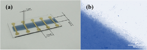
Figure 1. (a) Picture of a sample used in the determination of the sheet resistance via current versus voltage measurements. (b) Optical microscopy of the film edge with 50 × magnification.
Download figure:
Standard image High-resolution image2.3. Measurements
The film thickness profiles were measured in three different regions using a Dektak profilometer (model 150). With these measurements, we obtained the film thickness and the film uniformity considering the thickness variations throughout a wide region (~9.0 mm), including the film edges. The film roughness was measured using an atomic force microscope (AFM) Nanoscope Bruker, model 1203-A.
The resistance of the polymer blend films (RF) was directly determined by current versus voltage measurements using a Keithley 2410 High-Voltage Source Meter. To calculate the blend conductivity, σ, the geometrical parameters film thickness and width, t and w, respectively and the separation, s, of the electrodes had to be taken into account. The film thickness (in the range from hundreds of nanometers up to a few micrometers) was measured using a Dektak profilometer. The electrical conductivity (σ) was evaluated from the following relationship:
The sheet resistance, RS, of the polymeric thin films was determined from the resistance of films, RF, with different aspect ratio:

Where NS is the number of film surface squares used in the measurement (aspect ratio of the measurement).
The optical transmittance of the films in the visible range was measured by using a double-beam UV–Vis spectrophotometer Cary 50 Conc. The absorbance data allowed the determination of the film transmittance (T) by using the Beer–Lambert law:

where α is the material absorption coefficient.
2.4. Data analysis
The analysis of the data was performed by considering two extensive properties, optical transmittance and sheet resistance, and the production cost of the polymeric film on a figure-of-merit diagram. In this diagram, the optical transmittance of the polymeric films is a function of the inverse of the sheet resistance whereas a color scale represents the film production cost per unit area. The combination of equations (1)–(3) results in the theoretical relationship (equation (4)) for the transmittance and parameters which are independent of the film thickness (RS, α and ρ):
where ρ is the material electric resistivity. A mono-log plot for the transmittance versus the inverse of the sheet resistance exhibits an apparent linear behavior with the angular coefficient determined by the product of the intensive parameters α and ρ, which depends only on the blend composition. In order to determine the product αρ for different blend compositions a secondary figure-of-merit was proposed, describing the dependence of the product αρ on the PEDOT:PSS concentration. We also compare the intensive parameters of the blends with the material cost per unit mass and evaluate the product ( ) as function of the PEDOT:PSS concentration in order to establish the optimized blend composition that exhibits the best combination of optical transmittance, conductivity and cost.
The material and film production cost was evaluated considering the price of PEDOT:PSS provided by OSSILA (approximately US$80.00 g−1) and the price of PVA purchased from Sigma-Aldrich (approximately US$ 3.40 g−1).
3. Experimental results
The morphology of the top surfaces of the spray-deposited polymer films were inspected by optical microscopy, as seen from the micrographs presented in figure 2. Figures 2(a) and (b) show micrographs of the surface of a pure PEDOT:PSS film, in two different frame sizes, deposited by using the dispersion solution in the formulation as received from the supplier, whereas figures 2(c) and (d) present the micrographs of the blended film at 40% (wt) of PEDOT:PSS. One can observe that, in both cases, quite uniform films were obtained, and that, in the blended films, no phase separation can be noticed within the resolution of the method. In the micrographs displaying larger areas (figures 2(a) and 2(c)), few spot defects can be observed on the surface of both pure and blended films. From the micrographs, it is not possible to find out if these defects are pin-holes, superficial punctures or simply dust due the deposition at ambient conditions. However, in the present study, we are focusing on the electrical properties of the film in a planar direction and, considering that the defects occupy relatively small area of the film, we assume that these defects would not significantly affect the results presented herein. A further study concerning the influence of spray-deposition parameters on the film morphology to give rise to smoother film surfaces is considered as future work.
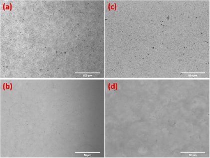
Figure 2. Optical microscopy images obtained from top surfaces of spray deposited films. (a) and (b) films produced with pure PEDOT:PSS. (c) and (d) blended films (PEDOT:PSS/PVA) produced with a PEDOT:PSS content of 40% (wt).
Download figure:
Standard image High-resolution imageFigure 3(a) shows the transversal profile of a film produced from the blend containing 40% of PEDOT:PSS. This profile shows that there is no significant thickness variation along the profile scan, including the edges defined by the shadow mask. The film uniformity was verified by performing profile measurements at several different regions of the film over the sample surface. These measurements have shown that the film thickness varies, in excess, 30%, which can be considered a reasonable value for manually spray-deposited films. This uncertainty in the film thickness was considered in the determination of the material conductivity, contributing to the final evaluated deviation. Figure 3(b) shows the AFM image obtained from a film produced with the blend containing 40% of PEDOT:PSS. The AFM images of several different regions, from different films resulted in a mean surface roughness of 110 ± 80 nm for all studied samples.
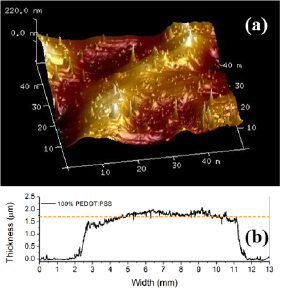
Figure 3. (a) AFM image of the top surface of a sample produced with the blend containing 40% of PEDOT:PSS and (b) transversal profile of the film.
Download figure:
Standard image High-resolution imageThe results from the electrical characterization of the produced films are depicted in figure 4. The current versus voltage (I–V) curves from a blended film (40% wt of PEDOT:PSS) embracing different aspect ratios in the structure of figure 1 (1 Sq, 2 Sq, 3 Sq and 4 Sq) are shown in figure 4(a). All the I–V curves exhibited a linear (ohmic) behavior, intercepting the axes at the origin, which was similarly observed for all studied blend compositions and aspect ratios. Figure 4(b) presents the electrical resistance of a blend containing 40% (wt) of PEDOT:PSS as a function of the film aspect ratio. The exhibited linear behavior proves that the film resistance is proportional to the increase of the aspect ratio (and to the film length), with the angular coefficient of the plot on figure 4(b) yielding the film sheet resistance RS.
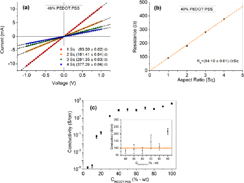
Figure 4. (a) Current versus voltage characteristic curves obtained from a blend containing 40% (wt) of PEDOT:PSS at different aspect ratios. (b) electrical resistance obtained from the results shown in (a) as function of the aspect ratio. (c) electrical conductivity of the blend as a function of the PEDOT:PSS/PVA weight ratio.
Download figure:
Standard image High-resolution imageThe sheet resistance and the electrical conductivity were evaluated for films based on different blend compositions. Figure 4(c) shows the dependence of the electrical conductivity on the PEDOT:PSS content in the blend. The results in the inset of the figure 4(c) show that, for PEDOT:PSS weight ratios between 40 and 80%, the electrical conductivity is nearly constant, presenting an average value around 100 ± 30 S cm−1, depending weakly on the PEDOT:PSS concentration. In contrast, the electrical conductivity of pure PEDOT:PSS films and films containing 90% of PEDOT:PSS were found to be about 480 ± 10 S cm−1 and 220 ± 20 S cm−1 respectively, whereas the conductivity of PEDOT:PSS/PVA blends at a 5% PEDOT:PSS concentration was considerably lower, around (2.0 ± 0.8) × 10−5 S cm−1.
Even though the electrical conductivity of blends with a PEDOT:PSS content between 40 and 90% is lower than the conductivity of pure PEDOT:PSS films, the loss in the electrical conductivity, concerning semitransparent electrode applications, is compensated by the increase in the optical transmittance in the visible range and the considerable decrease of the material cost. The light-absorption coefficient spectra of films with different blend component ratios are presented in figure 5(a). One observes a noticeable increase in the absorption coefficient with the PEDOT:PSS content in the blend, however, the variation is more abrupt when a 90% PEDOT:PSS film is compared to a pure (100%) PEDOT:PSS film. This behavior indicates that a content of only 10% (wt) of PVA in the blend composition, is enough to drastically change the material conductivity and light absorption.
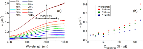
Figure 5. (a) Absorption coefficient obtained for samples with different PEDOT:PSS/PVA weight ratios as a function of the incident light-wavelength. (b) Absorption coefficient obtained for incident light at 595, 555 and 445 nm as function of the PEDOT:PSS/PVA weight ratio.
Download figure:
Standard image High-resolution imageFigure 4(b) shows the dependence of the absorption coefficient as a function of the PEDOT:PSS content in the polymer films at three different wavelengths: 595, 555 and 445 nm, which are, respectively, in the red, green and blue range of the visible electromagnetic spectrum, used in RGB additive colour model. Samples containing less than 30% of PEDOT:PSS exhibited low light-absorption coefficients in all three wavelengths due to the high transparence of PVA in the visible spectrum range. For blended films containing an amount of PEDOT:PSS between 30 and 90%, the absorption coefficient increases linearly with the PEDOT:PSS content in the blend. As previously observed, the absorption coefficient for pure PEDOT:PSS films behaves differently than for the blended films. This discrepancy presents the same trend as the abrupt variation on the electrical conductivity of pure PEDOT:PSS film compared to PEDOT:PSS/PVA blends with a high content of PEDOT:PSS (90%).
For applications as semitransparent conductive material in organic optoelectronic devices, the best combination of properties is given by a material with high optical transmittance (low absorption coefficient) and high electrical conductivity (low electrical resistivity). However, as can be concluded from the results presented on figures 4(c) and 5(a), it is not a straightforward task to determine the most appropriate blend formulation with optimal desired properties. To evaluate the balance of these two properties we propose to use the product of the light-absorption coefficient and the electrical resistivity (inverse of the conductivity) of the blended material as a function of the PEDOT:PSS content in the blend. The objective is to use a simple method to determine a blend composition which minimizes this product, i.e. which combines high conductivity and high optical transmittance. Figure 6(a) shows how the product α.ρ decreases with the PEDOT:PSS content in the blend, presenting quite high values for concentrations of PEDOT:PSS lower than 30%, meaning that formulations with ratios lower than that should be avoided for applications which demand high conductivity.
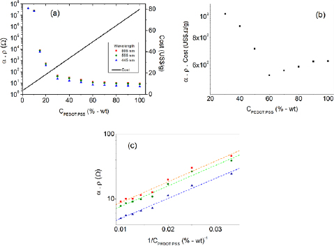
Figure 6. (a) Product of the absorption coefficient by the electric resistivity as a function of the PEDOT:PSS/PVA weight ratio and of the material cost as a function of the PEDOT:PSS/PVA weight ratio. (b) Product of the absorption coefficient by the electric resistivity and by the material cost as a function of the PEDOT:PSS/PVA weight ratio. (c) Product of the absorption coefficient by the electric resistivity as function of the inverse of the PEDOT:PSS/PVA weight ratio.
Download figure:
Standard image High-resolution imageThe material cost of the blended film, on the other hand, increases linearly with the PEDOT:PSS concentration, since it is considerably more expensive than PVA. In order to determine the optimum PEDOT:PSS/PVA blend composition that results in the best combination of conductivity, optical transmittance and cost, the product α.ρ.Cost was evaluated for different PEDOT:PSS concentrations (figure 6(b)). This plot presents a minimum value for PEDOT:PSS concentration of about 60%. Previous studies [43] on the mechanical properties of PEDOT:PSS/PVA blends have demonstrated that the optimum film flexibility (elongation break) is obtained for PEDOT:PSS concentrations below 40%. Taking into account the optical, electrical, blend cost and including the mechanical properties, it is reasonable to suppose that the optimum blend composition is obtained for a PEDOT:PSS content between 40 and 60%. In this range, lower PEDOT:PSS concentrations result in more transparent, low cost and flexible materials, whereas higher PEDOT:PSS concentrations result in more conductive materials.
The analysis of the separate intrinsic properties of a blended material can be used as a good indicator to find a suitable blend composition, however, it is still not sufficiently accurate to determine the best blend composition for a specific application. In the present paper, we propose the use of a figure-of-merit diagram, presented on figure 7, to identify the PEDOT:PSS/PVA blend composition and correspondent film thickness that produces semitransparent electrodes for flexible optoelectronic devices with a specific demand of optical transmittance, sheet resistance and cost. This diagram considers the dependence of the optical transmittance and the sheet-resistance with respect to the film thickness and PEDOT:PSS concentration (ranging from 30% up to 100%), as explained in section 2.3. In the considered concentration range, the product α.ρ follows the empirical relationship: α.ρ ∞ exp(−k/C), where C is the PEDOT:PSS content in the blend and k is a constant, which can be determined from the slope of the plots in figure 6(c). Two other empirical functions were employed to build the figure-of-merit diagram on figure 7. These fittings were performed using five order polynomials to describe the dependence of the blend electric conductivity and absorption coefficient as a function of the PEDOT:PSS concentration.
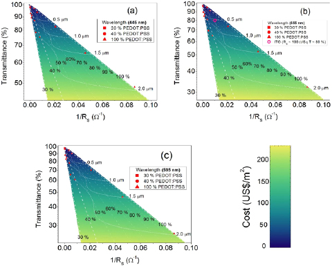
Figure 7. Optical transmittance versus the inverse of the sheet conductance diagrams for films produced with blends with a PEDOT:PSS content between 30 and 100% (pure PEDOT:PSS) in different regions of the visible spectrum. (a) 445 nm; (b) 555 nm (c) 595 nm.
Download figure:
Standard image High-resolution image
The fittings, obtained by employing equation (4), and the empirically determined αρ product as angular coefficient of the plots, exhibited good agreement with the experimental data. These empirical adjustments of the experimental data were useful to identify the film thickness-independent plots in the figure-of-merit diagram. Moreover, the polynomial fittings of the conductivity and absorption coefficient as a function of the PEDOT:PSS concentration were used to identify the PEDOT:PSS concentration-independent plots in the figure-of-merit. Therefore, this figure-of-merit diagram enables the design of semitransparent electrodes with a desired sheet resistance and optical transmittance (at a certain wavelength range) by controlling the PEDOT:PSS/PVA blend composition and the film thickness. The symbols displayed in figure 6 are the experimental data obtained from blends with 30%, 40% PEDOT:PSS content and from pure (100%) PEDOT:PSS films, in different film thicknesses.
The figure-of-merit diagrams can also be used as a guideline to design high performance semitransparent, flexible and conductive electrodes in the most inexpensive way. For example, ITO electrodes exhibit a sheet resistance of approximately 100 Ω sq−1 and optical transmittance of approximately 80% (at 550 nm). In figure 7(b) the ITO characteristics are depicted in the figure-of-merit, and are correspondent to a film with thickness about 750 nm, produced with the optimized blend composition (60% of PEDOT:PSS) with an approximate cost of US$ 40.00 per m2 of electrode. However, this blend composition is not the most flexible composition. The figure-of-merit shows that by employing the most flexible composition (produced with less than 40% of PEDOT:PSS) it is possible to fabricate electrodes with the same transmittance and cost, in spite of an increase of the sheet resistance to approximately 230 Ω sq−1 and film thickness to 1.5 µm.
4. Conclusions
Spray-deposited polymeric blends of highly conductive PEDOT:PSS and highly transparent and flexible PVA were produced and characterized aiming applications in electronic and optoelectronic devices as semitransparent flexible electrodes. We have observed that, by decreasing the PEDOT:PSS content in the blend (and, consequently, the material cost) down to 30% (wt), the electrical conductivity still remains acceptable for most of the applications in organic electronic and optoelectronic devices. We also demonstrate that, at a blend concentration of 60% (wt) PEDOT:PSS, optimal transmittance, electric conductivity and cost effectiveness is achieved. In order to establish a practical method to determine the optimal characteristics of PEDOT:PSS/PVA blends for flexible electrodes in organic optoelectronic applications, we introduced a figure-of-merit diagram which considers the optical transmittance, the sheet resistance, the production cost, the blend composition and the film thickness as empirical parameters which can be used to guide the film fabrication for a specific application. Depending on which film characteristic is more important for the aimed application, we have shown that a different combination of these parameters can be used, according to the figure-of-merit diagram, to find the most suitable blended film configuration.
Acknowledgments
The authors acknowledge the financial support obtained from FAPESP (Grants #2008/57706-4, #2012/19005-0 and # 2012/01624-5), CNPq, INEO and nBioNet, Brazil.
Biographies

Olivia Carr received a BSc in Physics in 2012 and AN MSc in Physics in 2015 from the Universidade Estadual Paulista Julio de Mesquita Filho, Rio Claro, Brazil. She is currently a PhD student at the University of São Paulo, São Carlos, Brazil. Her main interests are organic electronics, fabrication and characterizations of electroluminescent devices and biosensors for head and neck cancer detection.

Giovani Gozzi was born in São Paulo, Brazil, on 16 March 1984. He received a BSc degree in Physics from the Universidade Estadual Paulista (UNESP), Brazil, in 2005, MSc and PhD degrees in Applied Physics from the Universidade de São Paulo (USP), Brazil, in 2008 and 2011 respectively. He worked as a postdoctoral fellow at UNESP in 2013 and from 2014 to now, he is a Professor at Universidade Estadual Paulista, UNESP, at Rio Claro, Brazil. His research interests include organic electronics, charge injection and transport in organic semiconductors and electro-optical properties of organic light-emitting devices.

Lucas Fugikawa Santos was born on 18 November 1973 in Bastos, Brazil. He received a BSc degree in Physics in 1995 and MSc (1998) and Ph.D (2003) degrees in Applied Physics from the Instituto de Física de São Carlos (IFSC), Universidade de São Paulo, Brazil. He worked as a postdoctoral fellow at IFSC from 2003 to 2005 and as senior developing scientist at Optoeletronica S.A from 2005 to 2007. From 2007 to now, he is a Tenure Professor at Universidade Estadual Paulista, UNESP, at São José do Rio Preto, Brazil, where he is the leader of the Organic Optoelectronics Group. His major interests are charge generation, injection and transport in organic/polymeric semiconductors and physical characterization of electronic and optoelectronic organic devices.

Roberto Mendonça Faria is a Full Professor in the São Carlos Institute of Physics, University of São Paulo, where he has been a faculty member since 1977. He received his PhD (1984) in Physics at the University of São Paulo, in Brazil. Since the begining of the 1990s he has been involved in the field of organic electronics, then publishing more than 170 articles related to electric and optical properties of organic thin films and of organic electronic and optoelectronic devices. He supervised graduate degrees of more than 45 students. Now he heads the National Institute on Organic Electronics (INEO) that has more than 35 research groups throughout Brazil. He was director of the São Carlos Institute of Physics between 2002 and 2006, coordinator of the Institute for Advanced Study of USP/São Carlos (2010-1013), and is president of the Brazil Materials Research Society. He is member of the Brazilian Academy of Science and of the Academy of Science of São Paulo State

Dante Luis Chinaglia was born in São Carlos City, São Paulo State, in 1959. He orked in the Physics Department of Universidade de São Paulo, São Carlos from 1978 up to 1988 in research technical support. In 1990 received a Physics BS degree from Universidade de São Paulo, São Carlos. In 1992 the M.S degree in Applied Physics and in 1999 the Ph.D. degree in Materials Science and Engineering bolt from Universidade de São Paulo, São Carlos. In 1994 he started work as a Professor at Universidade Estadual Paulista. From 2010 up to 2014 he was the Head of the Physics Department of Universidade Estadual Paulista, Rio Claro city, and in 2011 received the degree of abilitation (Senior Professor). Works mainly with the charge transport in insulating and conductive polymers, phase transition in the PVDF and light-emitting devices based on organic/inorganic hybrid materials.