Abstract
Electron transport through a single C60 molecule on Cu(1 1 1) has been investigated with a scanning tunnelling microscope in tunnelling and contact ranges. Single-C60 junctions have been fabricated by establishing a contact between the molecule and the tip, which is reflected by a down-shift in the lowest unoccupied molecular orbital resonance. These junctions are stable even at elevated bias voltages enabling conductance measurements at high voltages and nonlinear conductance spectroscopy in tunnelling and contact ranges. Spectroscopy and first principles transport calculations clarify the relation between molecular orbital resonances and the junction conductance. Due to the strong molecule–electrode coupling the simple picture of electron transport through individual orbitals does not hold.
Export citation and abstract BibTeX RIS

Content from this work may be used under the terms of the Creative Commons Attribution 3.0 licence. Any further distribution of this work must maintain attribution to the author(s) and the title of the work, journal citation and DOI.
For more information on this article, see LabTalk.
1. Introduction
The transport of electrons through atomic-scale contacts between two electrodes may be interpreted in terms of transport channels—quantum states extending between the electrodes—and their transmission probabilities τn [1]. In calculations, these probabilities vary drastically as a function of the electron energy [2–5]. Experiments have addressed the low-bias conductance [2, 6–14] and therefore typically provided little information on the transport channels and their τn. Metallic contacts between superconducting leads are a notable exception. In this case, Andreev reflections have been used to experimentally determine the τn at low bias [2, 6, 7]. However, experimental data on the variation of τn with the electron energy E were not reported.
Molecular junctions are expected to exhibit more and sharper structure of τn(E) [15]. The energy gap between occupied and unoccupied states of many molecules used in contact experiments is of the order of electron volts. As a result, probing their contributions to the conductance at contact is difficult. At the required elevated voltages and correspondingly large currents heating of the junctions occurs [16–19] and may lead to their destruction [17]. In a previous break-junction experiment the number of transport channels in benzene junctions has been determined using shot noise measurements [20]. To date, hardly any experimental data are available for highly conductive molecular junctions [20, 21].
Here, we report results from single-molecule contacts to C60 on Cu(1 1 1). Owing to a C60-induced reconstruction the contacts are stable enough for conductance spectroscopy [G(V)] at elevated bias voltages. Conductance resonances are observed and quantitatively analyzed using first-principles calculations. As expected, the molecular orbitals leave their footprint on G(V). However, it turns out that a picture of parallel transport through individual orbitals is too simple and only accounts for a fraction of the total conductance.
2. Experiment
Experiments were performed with a scanning tunnelling microscope (STM) operated at 8 K and in ultrahigh vacuum with a base pressure of 10−9 Pa. Chemically etched W tips and Cu(1 1 1) surfaces were cleaned by Ar+ bombardment and annealing. C60 molecules were sublimated from a Ta crucible and adsorbed to clean Cu(1 1 1) at room temperature. After C60 deposition the surface was annealed at 500 K for 10 min. This preparation leads to the formation of well ordered C60 islands and a reconstruction of the Cu(1 1 1) surface [22]. To form a single-molecule contact the STM tip was brought closer towards the center of a molecule and the current was simultaneously recorded. Before and after contact experiments STM images and spectra of the differential conductance (dI/dV) were recorded to detect tip or molecule modifications. It turned out that the junctions are stable up to currents of ≈20 µA at elevated voltages of ≈1 V. Spectroscopy of dI/dV was performed by modulating the sample voltage (10 mVrms, 8 kHz) and measuring the current response with a lock-in amplifier.
3. Theory
To simulate experimental data, tunnelling and contact junctions were modelled by a tetrahedral Cu tip attached to a 4 × 4 surface unit cell in a 7-layer Cu slab (substrate) and a C60 molecule adsorbed with a C hexagon to an on-top Cu(1 1 1) site (inset to figure 3(b)). The electronic structure, contact formation and conductance of the C60 junction were calculated within density functional theory (DFT) with the generalized gradient approximation (GGA-PBE) [23] to the exchange-correlation functional and a 2 × 2 surface k-point sampling. A localized atomic orbital basis set (SIESTA) [24] as well as a plane-wave basis set (VASP) [25] were used in order to access and avoid basis set superposition errors, which are present in calculations based on the linear combination of atomic orbitals. A series of calculations were performed in which the tip and the surface were approached towards each other in steps of 0.1 Å by decreasing the unit cell dimension in the approach direction. Relaxations of the tip tetraeder, the C60 molecule, and the two outermost surface layers were considered in these calculations. The TRANSIESTA [26] method was then applied to perform transport calculations of the linear conductance as well as non-equilibrium calculations of the current–voltage characteristics for two selected junction configurations in the tunnelling and contact range.
4. Results and discussion
The inset to figure 1 shows a constant-current STM image from the interior of a C60 island. Similar to previous observations from other surfaces [27–30], the molecules exhibit three protrusions, which are due to the next-to-lowest unoccupied molecular orbital (LUMO + 1). This orbital is centred at the three C pentagons that surround a hexagon in the observed trifoliate way. When the tip is brought closer to a molecule the conductance varies as displayed in figure 1(a). Tunnelling, transition and contact ranges are defined using the intersections of exponential fits to the conductance data (indicated in the lower curve of figure 1(a)) [31]. The two data sets shown were recorded at sample voltages V = 0.5 V and 1.5 V and exhibit different conductances Gc at the transition to contact, namely ≈0.15 G0 and ≈0.25 G0, respectively.
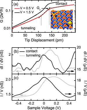
Figure 1. (a) Conductance of C60 on Cu(1 1 1) in a STM versus displacement of the tip towards the molecule. Red and black lines indicate data recorded at sample voltages V = 0.5 V and 1.5 V, respectively. Dashed lines illustrate the definition of the point of contact formation and the corresponding conductance Gc. Vertical lines separate different conductance ranges, namely tunnelling, transition, and contact. Inset: pseudo-three-dimensional representation of a constant-current STM image of a C60 monolayer on Cu(1 1 1) (1.5 V, 100 pA, 6 × 6 nm2). (b) dI/dV and (c) I/V curves as a function of V acquired at fixed tip heights in the tunnelling range (grey) and at contact (black). Tip heights were set by disabling the STM feedback loop at 0.6 V and, respectively, 0.7 nA and 11.6 µA in tunnelling and contact ranges. The small sharp feature at V = 0 in (c) is a numerical artefact.
Download figure:
Standard image High-resolution imageTo relate the bias dependence of the conductance to the electronic structure of the adsorbed molecule, dI/dV spectra were acquired at constant tip–sample separations. The grey and black lines in figure 1(b) show data sets from the tunnelling and contact ranges, respectively. In the tunnelling range constant-height dI/dV spectra of C60 can be routinely recorded over a fairly wide range of bias voltages. At contact, however, currents on the order of 10 µA flow and the junction usually becomes unstable at much lower voltages. Owing to the particular stability of the structures used here, the range from −0.5 to 0.5 V can be probed. The tunnelling data of figure 1(b) show a peak centred at ≈100 mV. Previous reports have shown that it is due to the C60 LUMO [22, 32]. At contact, a similar peak is observed, albeit broadened and shifted to ≈0 mV. Our calculations (vide infra) reveal a hybridization of C60 with the tip. It is not clear that the contact data may simply be interpreted in terms of a density of states of the junction. Ignoring this issue for the moment, we find that the differences of the contact spectrum are consistent with the calculated electronic structure of the junction. Figure 1(c) shows the conductances G = I/V, which were recorded along with the dI/dV spectra.
To extend the accessible range of voltages at contact, a different method was used. Rather than sweeping the voltage at a fixed tip–molecule distance, the current was recorded as a function of the tip height while keeping V fixed. The conductance Gc at contact formation was then extracted as described above (figure 1). The results are depicted in figure 2 (black) together with a constant-height tunnelling dI/dV spectrum (grey). Over the investigated voltage range −2 V ⩽ V ⩽ 1.6 V, the contact conductance Gc varies significantly between 0.07 G0 and 0.26 G0. Moreover, the maxima at V ≈ 0 V and ≈1.5 V) are close to maxima of the tunnelling dI/dV data at ≈100 mV (LUMO) and ≈1.3 V (LUMO + 1).

Figure 2. Contact conductance Gc (black) and tunnelling dI/dV data (grey) versus sample voltage. Gc has been extracted from individual conductance-versus-displacement curves (see figure 1(a)) acquired at voltages between −2 V and 1.6 V.
Download figure:
Standard image High-resolution imageDFT calculations based on the structure shown in the inset to figure 3(b) were performed to rationalize the experimentally observed shift of the LUMO resonance to lower energies upon the tunnelling-to-contact transition. Figure 3 shows the zero-bias transmission functions calculated with a 9 × 9 surface k-point sampling. The peak-like structure close to the Fermi energy (EF) is due to the LUMO resonance, which clearly shifts towards EF upon decreasing tip–C60 distances and thus increasing hybridization. According to a Bader charge analysis based on the VASP calculations [33] a charge of ≈0.4 e is transferred from the tip to the molecule. For large tip–molecule distances in the tunnelling range the transmission function exhibits an approximate exponential variation with the distance. The contact formation may be observed as a deviation from this scaling behaviour due to the onset of chemical interactions leading to a resonance shift and broadening. Such deviations are indeed present for a tip–hexagon distance between 2.3 and 2.7 Å with a corresponding conductance of ≈0.2 G0. According to the experiments the contact conductance close to zero bias voltage is ≈0.16 G0 (figure 2). For tip–molecule distances at which repulsive interactions start to deform the tip apex into a flat geometry the conductance is close to 0.3 G0. At positive energies, starting from ≈0.4 eV the tail of a second transmission resonance has been observed in the calculations (figure 3).

Figure 3. Transmission functions calculated using relaxed geometries obtained from SIESTA (a) and VASP (b) with PBE-GGA labelled by the unrelaxed tip–C60 distances measured from the tip apex atom to the C hexagon plane. Beyond contact formation at 1.7 Å (unrelaxed distance) the relaxed tip–C60 distance hardly changes. Instead the tip is progressively compressed in both SIESTA and VASP calculations. The transmission functions show the change of the C60 LUMO resonance close to the Fermi energy (EF) at zero bias during contact formation. A clear lowering of the resonance energy towards EF is observed (vertical arrows). The functional form of the transmission versus energy roughly shows an exponential decrease in magnitude with increasing tip–C60 distance in the tunnelling range starting from ≈2.7 Å. The inset to (b) shows the structural model of the junction used in the calculations.
Download figure:
Standard image High-resolution imageFigure 3 compares results using geometries obtained from SIESTA (figure 3(a)) and VASP PBE-GGA (figure 3(b)) calculations. Both methods lead to virtually identical evolutions of the energy-dependent transmission functions. In the SIESTA calculations the tip apex atom is slightly stretched towards the C60 molecule upon approaching the tip to the surface. Further approach of the tip leads to a repulsive tip–molecule interaction and deforms the tip apex towards a flat geometry. Including van der Waals forces in the VASP calculations [34] (not shown) did not lead to markedly different conductance behaviour with tip displacement. While the calculated conductances in the contact range are in good agreement with the experimentally observed values, the calculated exponential variation of the conductance with the tip–molecule distance in the tunnelling range is somewhat larger than in the experiments. This observation is probably due to the use of an atomic basis set description of the tip [35]. In addition, as is evident from figure 1(a) the slope of conductance-displacement characteristics depends on the bias voltage both in tunnelling and contact ranges. Thus, the bias voltage plays a significant role in the effective tunnelling barrier as well as in the contact formation. This effect could likewise involve bias voltage-induced atomic relaxations. In the calculations we neglect the computationally very demanding bias-induced relaxations but note that these can lead to significant forces in the contact range [19].
Next, full non-equilibrium calculations based on the junction geometries obtained from SIESTA were performed. The resulting bias voltage-dependent conductances at contact in figure 4 (black) displays much similarity with the experimental data (grey). A resonance with ≈1 V full width at half maximum is centred around 0 V. In addition, resonances are observed in the calculations for negative and positive bias voltages, which are similar to the experimental results.

Figure 4. Comparison of experimental Gc (grey) and calculated conductances (black). In the calculations the tip apex atom was separated by 2 Å from the closest C60 hexagon.
Download figure:
Standard image High-resolution imageFigure 5 shows how these transmission maxima change with the sample voltage. As expected from the strong C60–Cu(1 1 1) coupling, the maxima essentially follow the sample chemical potential, which is defined as −eV/2 with V the sample voltage. Slight deviations from the evolution of the sample chemical potential are due to a small coupling between the molecule and the tip. As exposed in detail next, the notion of individual molecular states and their identification with transmission maxima requires some caution due to the strong molecule–electrode coupling. Allowing only transport via the highest occupied molecular orbital (HOMO), LUMO, or LUMO + 1 states of the molecular region in the calculation does indeed warrant this designation. However, the simple picture of parallel transport via each of these orbitals only accounts for a fraction of the total transmission, as demonstrated below.
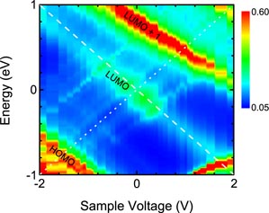
Figure 5. Density plot of the transmission function, T(E, V) = ∑nτn(E, V), for different energies E and voltages V in the contact range. The energies of the transmission maxima labelled HOMO, LUMO, and LUMO + 1 approximately follow the chemical potential of the sample −eV/2 (dashed line). Weaker transmission features are related to tip states and follow the chemical potential of the tip (+eV/2, dotted line).
Download figure:
Standard image High-resolution imageThe standard Green function expression [26] for the elastic transmission, T, reads

where G is the retarded Green function matrix and ΓL/R the electrode coupling matrices in the full basis set describing the scattering region. The transmission eigenchannels τn, with T(E) = ∑nτn(E) (figure 6(a)) [15], provide an exact decomposition of the total transmission, but do typically not show a separation into molecular orbitals. The dominant transmission eigenchannel (black line in figure 6(a), transmission probability τ1(E)) closely follows the C60 HOMO, LUMO, and LUMO + 1. The single channel giving rise to the LUMO transmission is due to the coupling of the rotational symmetric s orbital on the tip around the Fermi energy. Close to the LUMO + 1 energy (≈0.9 eV) three channels contribute to the conductance.
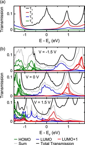
Figure 6. (a) Eigenchannel transmissions, τn(E) (n = 1, ..., 4), at zero bias for the contact range (tip–C60 distance: 1.9 Å) averaged over all k points. The dominant transmission channel (black, transmission probability τ1(E)) closely follows the C60 HOMO, LUMO, and LUMO + 1. Around the energy of the LUMO + 1 (≈0.9 eV) three channels contribute to the conductance. (b) Orbital-projected transmission functions Tα(E) for the C60 HOMO (green), LUMO (blue) and LUMO + 1 (red) resonances evaluated at the indicated voltages (tip–C60 distance: 1.9 Å, i.e. in the contact range). Several contributions are observed from each orbital due to their partial degeneracy. The grey line depicts the sum of all transmissions, ∑αTα(E), while the solid black line is the total transmission calculated according to equation (1).
Download figure:
Standard image High-resolution imageTo test whether transport takes place in parallel via molecular orbitals of C60 the eigenstates of the molecule-projected self-consistent Hamiltonian (MPSH) [36] were calculated, which correspond to the HOMO, LUMO, and LUMO + 1. The coupling matrices in equation (1) were then projected onto each of these orbitals in order to evaluate the transmission probability of electrons that enter and exit the C60 junction via one of these orbitals. The projected electrode couplings read
 , where α is one of the molecular orbitals and Pα a corresponding projector for the same subset region. Using
 in equation (1) the resulting Tα,

is interpreted as the electron transmission via orbital α. Therefore, Tα(E) may be used to judge the extent to which the assignment of individual orbitals to a specific transmission feature is valid. Figure 6(b) shows the k-averaged transmission functions Tα(E) for the HOMO (green), LUMO (blue) and the LUMO + 1 (red) at bias voltages of −1.5 V (top), 0 V (middle), +1.5 V (bottom). The fivefold (threefold) degeneracy of the HOMO (LUMO, LUMO + 1) of the free C60 molecule is partly lifted for C60 attached to the electrodes. Each degenerate orbital contributes to the transmission. The sum of all transmission curves is plotted as a grey line.
It is clear from figure 6(b) that the projected transmissions of the HOMO, LUMO, and LUMO + 1 do indeed follow the main peaks in the total transmission. The shift of individual transmission peaks to lower energies with increasing bias voltage (figure 5) is also visible. However, the projected transmissions of HOMO, LUMO, LUMO + 1 do not add up to the total transmission (black line in figure 6(b)) in the energy range where we expect the conductance to take place in these. Mostly the sum of projected transmissions (grey line) is lower than the total transmission (black line)4. In figure 6(b) we have restricted the calculations to the HOMO, LUMO and LUMO + 1. It is necessary to include more molecular orbitals in the sum to obtain peaks farther from EF. For instance, in figure 6(b) the total transmission peaks for energies exceeding 1 eV cannot be accounted for by the contributions from the chosen projected orbitals (grey line) and would require inclusion of the LUMO + 2. For obtaining the full picture the off-diagonal contributions from different α in equation (2) must be considered. Electrons enter and exit the molecule via different orbitals α, α' and may play a significant role for the transmission. Due to the strong molecule–electrode coupling the resonances originating from the molecular orbitals have weight inside the metal and mix with each other. The terms that describe the mixing are mainly positive leading to a lower sum of projected transmission. Occasionally they are negative which leads to a higher projected transmission at certain energies. The mixing can be quantified by the corresponding off-diagonal transmission,

where α and α' are different. In figure 7 we show the transmission for the LUMO and the LUMO + 1 with (full lines) and without (dashed lines) the mixing with nearby orbitals including HOMO, LUMO, LUMO + 1. Including the mixing yields a significant contribution and thus mixing between orbitals due to the strong coupling in the junction plays a significant role. Thus we conclude that the approximation of parallel transport through individual C60-states neglects significant contributions to the conductance.

Figure 7. Contributions to LUMO and LUMO + 1 transmissions from diagonal (dashed lines) terms (α = LUMO, LUMO + 1 in equation (2)), and off-diagonal/mixing (full lines) contributions to the LUMO, LUMO + 1 transmission from nearby orbitals (HOMO, LUMO, LUMO + 1) (equation (3)).
Download figure:
Standard image High-resolution image
5. Conclusion
Conductance spectroscopy and first-principles transport calculations clarify the role molecular orbital resonances play in determining the conductance of a molecular junction at contact. A picture of electron transport through individual orbitals [2, 37] does not hold. Rather, for strong molecule–electrode couplings mixing of orbitals must be considered for the correct description of the junction conduction.
Acknowledgments
Financial support by the Deutsche Forschungsgemeinschaft through SFB 677 is acknowledged. We thank T Frederiksen (San Sebastian) for useful comments and the DCSC for computational resources.
Footnotes
- 4
At some energies the sum of projected transmissions occasionally exceeds the total transmission, which is due to interference phenomena.