Introduction to digital logic
Published September 2017
•
Copyright © 2017 Morgan & Claypool Publishers
Pages 1-1 to 1-17
You need an eReader or compatible software to experience the benefits of the ePub3 file format.
Download complete PDF book, the ePub book or the Kindle book

Permissions
Abstract
This chapter covers the (theoretical) concepts of digital logic. Digital gates are introduced and different representations, such as Boolean logic, schematics and truth tables are shown. Boolean logic rules are derived and the chapter ends with examples on implementing digital designs.
Additional reading
Read pages 703–24 in Horowitz P and Hill W 2015 The Art of Electronics 3rd edn (New York: Cambridge University Press) and pages 717–37 in Scherz P and Monk S 2013 Practical Electronics for Inventors 3rd edn (New York: McGraw-Hill Education).
1.1. Basic definitions of digital concepts
1.1.1. Definition
While an analog signal is continuous, a digital one is discrete. Specifically, an analog signal represents an infinite continuum of levels while the digital one represents finite, discrete levels.
1.1.2. Analog versus digital analogy
Our world is inherently analog. We sense continuous signal levels such as the intensity of light or sound. In contrast, if humans were born with digital sensory organs we would only sense binary states, for example brightness or darkness, silence or noise. Not surprisingly, most of us who are fortunate to enjoy functioning analog sensory organs would never want to trade these for digital ones. Based on this observation it appears that in comparison to analog, digital technology is inherently limited and crude. Nevertheless, the prevailing trend in technology clearly favors the digital approach over the 'old' analog one, indicating significant advantages of this 'new' technology. Let's explore the main advantages with the following analogy.
Imagine that you are in a concert hall with two 'musicians' who are hidden from the audience by a curtain. The task for the performers is simple: they are each asked to play a single note on their instrument and then the audience is asked to describe the sound intensity or if they even heard that instrument was played.
After the first performer plays a few identical notes on a violin you probably would get a wide response from the listeners ranging from 'quiet' to 'loud'. After all, the perception is subjective and based on the listener's music preference, hearing capability and distance from the player. Furthermore, depending on the relationship between how loud the note was played and how loud the background noise was in the hall, it may even be hard for the listeners to discern the state of the instrument, i.e. was it played at all or did they only hear noise.
Next imagine the second player, who uses an extremely loud and obnoxious sounding car horn as his instrument. Again he plays one note by turning the horn on or off multiple times. Now, most listeners would clearly agree on the state of the perceived sound intensity, i.e. either it was quiet or loud—the horn was 'on' or 'off'. As long as the car horn is louder than the background noise level in the concert hall (a very likely condition) no ambiguity of the signal state exits.
If our only concern is to make certain that the audience perceives the signal's state, i.e. is the instrument being played or not, then clearly the second musician with his digital approach wins. By using an instrument capable of only producing two clearly discernable states, complete silence and ear piercing noise, he is able to transmit his message across the concert hall without ambiguity or errors. It should come as no surprise why this digital message system works so well; after all, it was designed to work in an extremely noisy environment, such as traffic, to deliver a clear (warning) message.
In summary, by only using clearly identifiable states, digital technology is able to transmit a signal state that is (almost) immune to noise. By the same reasoning, it follows that these states can also be duplicated and stored without degradation by ambient noise. In digital technology, such a binary 'signal' is referred to as a 'bit' and its state as 'on' or 'off'.
Of course, one could make the argument that we are really comparing two completely different systems in our concert hall analogy. It is one thing to convey a clear message by, for example, either remaining completely quiet or blasting an obnoxious car horn. However, it is a completely different matter to convey a more complex, nuanced and probably esthetically pleasing message, such as the violinist may produce with her analog instrument. Instead, the question we should ask is: can we produce a more nuanced message with our simple car horn? At first, this may seem impossible if we are only allowed to use the two clearly discernable states that our car horn emits, silence and noise. However, the digital world gets around this issue by 'bundling' bits into a package and then assigning meaning to this sequence of bits. This is actually not all that different from the way some drivers operate their car horn: no honking means you are ok; one brief honk means you have mildly irritated someone; a long series of honks clearly means you should get off your phone. While this is a bit oversimplified, it shows that we can express a discrete level of emotions by using only silence and no silence.
It also highlights another aspect of digital technology, namely that the more signals, or bits, we agree to use in our sequence, the finer we can express these levels. However, as long as we are forced to use a finite sequence of bits, the number of levels we can express will also be finite. Going back to our traffic analogy, while with one bit we can only express two levels, 'ok' or 'angry', with just two bits we can signal four levels, 'ok', 'mildly irritated', 'somewhat irritated' and 'angry'.
Another advantage that digital technology has over analog is the ease with which the data can be manipulated using very simple 'operators', called gates, to mimic mathematical operations.
In summary, the high noise immunity of transmitting and storing digital signals and the ease with which they can be manipulated with mathematical operations give digital an advantage over analog. This explains the current trend away from analog and towards digital technology. Nevertheless, you should keep in mind that we started out by saying that our world (including us humans) is inherently analog. Therefore, at least as long as humans have no digital ports, we will always be working with both analog and digital technology and the interface between these two worlds, analog-to-digital and digital-to-analog converters.
1.1.3. Binary states and digital logic levels
When we refer to the binary state of a bit we will use the conventional labels of 'on' or 'off', '1' or '0' or 'high' or 'low' (which is sometimes also written as 'HI' or 'LO'). We will use these labels interchangeably and agree that 'on', '1' and 'high' are considered equivalent and so are 'off', '0' and 'low'.
In a physical environment, such as an electronic circuit, explicit voltage or current level standards exist for a specific digital logic state. Multiple conventions exist and the most common ones are listed in table 1.1. To conserve energy and to increase switching speeds, the 3.3 V low voltage transistor–transistor logic (TTL) standard is increasingly replacing the old, established 5 V TTL level.
Table 1.1. Most commonly used digital voltage standards.
| Logic level | 3.3 V CMOS OR TTL | 5 V TTL |
|---|---|---|
| 1, on, high | 3.3 V | 5 V |
| 0, off, low | 0 V | 0 V |
Table 1.1 is deliberately kept simple and it does not list the acceptable threshold levels for high and low input and output signals. Typically these are within one volt of the 'ideal' levels listed above. For example, for the 3.3 V CMOS systems, an input voltage between 0 and 0.8 V is acceptable as a low input, signals between 2.0 and 3.3 V are considered as a high input; you want to avoid input signal levels between 0.8 V and 2.0 V because they are ambiguous.
Discrete components require external power and the levels listed above state their supply voltages.
Finally, avoid applying input signals exceeding the high or low levels stated above. Doing so can destroy the components!
1.1.4. Manipulating digital logic levels with operators or gates
As mentioned previously, the power of digital logic comes from the ability to manipulate the signals through logic gates. These logic gates are to digital technology what operators are to mathematics. There are only three fundamental gates: the NOT, AND and OR gates. All other gates and the entirety of digital technology are based on repeatedly applying these three operators in various combinations. While this may be hard to believe, remember that a large part of mathematics is composed of repeated applications of the addition and subtraction operator, resulting essentially in multiplication and division. As you will see later, by combining these gates you will be able to build a simple calculator, a music player and even a microprocessor.
1.2. Digital and Boolean logic and its representation
Multiple methods exist to represent digital logic, each having its strengths and weaknesses. Working with digital designs requires the ability to move fluently from one representation to the next.
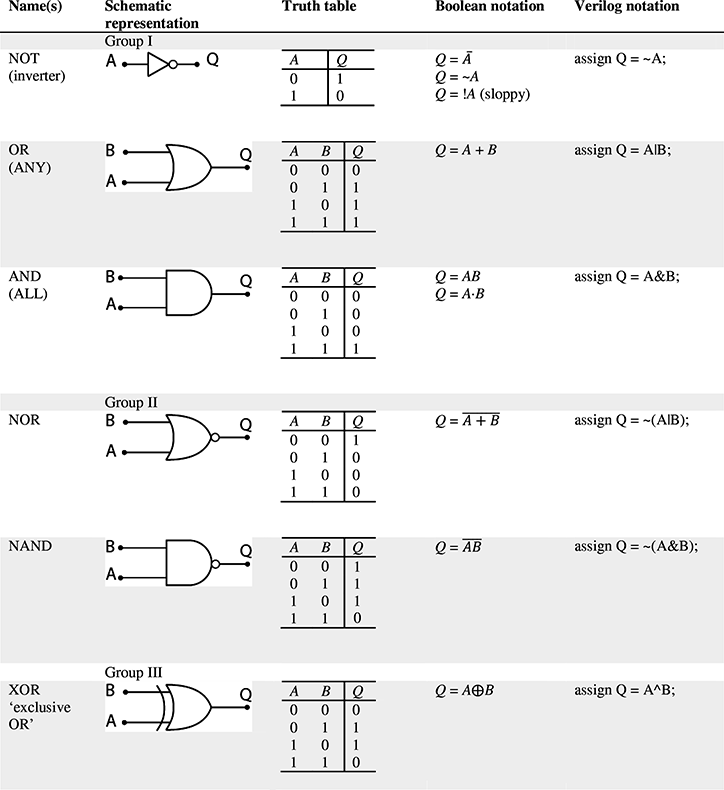
All the basic gates and four corresponding representations are shown in table 1.2. In these examples, A and B are inputs and Q is the output.
Table 1.2. Table of equivalent digital logic representations.
|
We augmented the three fundamental gates in group I with three additional gates. The gates in group II, the NOR and NAND gates, are a combination of either an OR or an AND gate with a NOT gate. The XOR gate in group III is a combination of all three fundamental gates. These additional three gates are used so frequently that they have been awarded their own name and symbol.
Before we look at the individual gates in more detail, let's briefly discuss the individual logic representations.
Schematic representation. This representation is useful when creating a detailed schematic diagram of a logic circuit and aids in pin assignments and debugging.
Truth table. A truth table lists every possible input combination and its resulting output. It provides a complete state-map of the component. By applying the truth tables to each circuit element and propagating the outputs to the next input you can (theoretically) always predict the behavior of any circuit. In reality, with large designs this approach can quickly become tedious.
Boolean logic. This representation is similar to algebraic notation although it has its own set of rules. Similar to algebraic expressions, Boolean logic expressions can be rearranged and simplified. When you work with them keep in mind that a fairly wide range of notations exists for the operators which can easily cause confusion. Also, be aware that some of the operators look similar to mathematical operators but they behave very differently in Boolean logic.
Verilog representation. Verilog is an officially sanctioned ANSI hardware descriptive language (HDL). Therefore, its notation has to be precise and unambiguous. It is very unforgiving and a typo can lead to unanticipated outcomes.
Venn diagrams. The Venn diagrams, sometimes also called Johnston diagrams, for a NOT, an OR and an AND gate are shown on the right-hand side of figure 1.1. The notation is based on set theory and can be used as yet another representation of digital logic. Similar to a truth table, it lists all possible input combinations with the first digit corresponding to the first input and the second digit to the second input. The dark shaded areas correspond to the regions resulting in a true output state for the particular logic operation shown. Venn diagrams are of limited use, in particular in larger circuits, and we will not use them any further.

Figure 1.1. Venn or Johnston diagrams for a NOT, OR and an AND gate..
Download figure:
Standard image High-resolution image1.2.1. Fundamental gates
The three fundamental gates of digital logic are the NOT, OR and AND gate.
The NOT gate is an inverter. It negates the current state and switches it to its opposite. For example, by NOT being 'on', something is 'off'. (Note: the NOT operator is sometimes written as , ∼X or !X. As you will see later, if X represents a collection of bits then the meanings of ∼X and !X are not equivalent. Avoid the confusion and stick with ∼X.)

Applying a NOT operator successively an even number of times results in no change since every other NOT operation cancels the previous one. For example, applying the NOT operator twice as in: results in . A schematic representation of this expression is:


Download figure:
Standard image High-resolution imageThe NOT operator symbol is often drawn in an abbreviated form, omitting the triangle and using only the open circle at its end. The three circuits below illustrate this. All three circuits depict the functionality of a NOR gate, i.e. an OR gate followed by a NOT gate:

Download figure:
Standard image High-resolution imageThe same abbreviated form of a NOT gate is also used at the gate inputs, as depicted in the three circuits below. The circuits represent a 'NOT A, NOT B, OR-gate' (of course, the functionality of these three circuits is not equivalent to the three circuits shown directly above!):

Download figure:
Standard image High-resolution imageThe remaining fundamental gates are the OR and the AND gates. Unlike the NOT gate which is a unary, single-input operator, both the OR and AND gates have at least two inputs.
First, note the commutative nature of these gates, and Boolean logic in general, shown below:

Download figure:
Standard image High-resolution imageAlthough the gates shown above are two-input gates, we could easily expand their inputs to any number while maintaining their functionality. An example of a three-input OR gate is shown below. The circuit on the right is displayed in its concise form while the one on the left details its implementation with two-input OR gates. This approach could be extended further and it works for any two-input gate. Note that we implicitly made use of the Boolean associative properties, namely:

Download figure:
Standard image High-resolution imageFinally, let's examine the difference between the OR and AND gates with the following two examples.
In the first example, assume that you have 1000 individual particle detectors and you want to monitor when at least one of them has been activated. Assume that when an individual detector is hit by a particle, the detector's output goes high. The easiest way to look for such an event is to connect all the particle detector outputs to one giant OR gate (having 1000 inputs) and monitor its (single) output. When the OR gate's output goes high, we know that at least one particle has passed through one of the detectors. In other words, the OR gate goes high when any one of its inputs goes high. This is the reason the OR operator is also known as the 'ANY' operator.
For the second example, consider that we are trying to locate a mysterious source of particles originating somewhere in the universe, far away. We will use a particle 'telescope' to detect their origin. It works similarly to an optical telescope, except that it employs a number of particle detectors in place of lenses, arranged in a straight line. We can pinpoint the particles' origin by sweeping our telescope across the sky and monitoring for an event when all our detectors are activated at the same time. This occurs only when all the detectors are aligned with the mysterious source. (In this example, we assume that the particles travel in a straight line and close to the speed of light.) This technique, often called an n-fold coincidence technique, where n refers to the number of detectors placed in coincidence, can be implemented by connecting all the detector outputs to the input of a giant AND gate. The output of the AND gate will go high only when ALL the inputs are high, meaning that we must have aligned our detectors in the direction of the source. This example illustrates the finicky nature of AND gates: unlike the 'combiner' OR gates, AND gates are very selective and act like a 'filter'. Since all its input conditions must be satisfied for its output to go high, an AND gate is sometimes called an 'ALL' gate.
Finally, a quick word on Boolean notation for these two gates: the OR operator is usually expressed by using the addition symbol, +. However, Verilog does have an addition operator and this can lead to confusion since the behavior is different. This will be discussed in more detail later. In Boolean notation, the AND operator is often omitted and it is implicitly understood that AB really means A · B.
1.3. Basic Boolean logic rules: application and examples
The diagram in figure 1.2 shows the output from various gates based on the time-dependent input of A and B. In this timing diagram the x-axis represents time and the y-axis the digital voltage level. (Note: the last trace shows the output from an XOR gate.)

Figure 1.2. Time dependent output for an OR, AND and XOR gate as a result of input signals A and B.
Download figure:
Standard image High-resolution imageExample 2: deriving basic Boolean logic rules from truth tables
Let's apply the truth tables from table 1.2 to derive some fundamental Boolean logic rules. See if you can work out the conclusion from the expression on the left by using the truth tables for the particular gate.
Table 1.3. This table lists some basic Boolean expressions and their corresponding schematic representation. It utilizes truth tables to obtain the resulting state.

|
1.4. Interchangeability of gates and De Morgan's theorem
In the previous exercise, we simplified Boolean expressions and eliminated redundant components. This section will use the truth tables and show that we can mimic the behavior of one type of gate by substituting it with a different type or types. In other words, we will develop Boolean rules on how to interchange gates.
Example 1. NOT gate from a NAND gate
Shown below is a NAND gate with its inputs tied together. When you examine its truth table (below), you notice that it functions as an inverter! Note that the same result could have been obtained by using a NOR gate in a similar configuration.

Download figure:
Standard image High-resolution image| A | B = A | AA | |
|---|---|---|---|
| 1 | 1 | 1 | 0 |
| 0 | 0 | 0 | 1 |

Conclusion: you can substitute a NOT gate with a NAND or NOR gate whose inputs have been tied together. However, you can never create a NOT gate from an AND or an OR gate alone. (Proof left to the reader.)
Example 2. AND gate from NAND gate

Download figure:
Standard image High-resolution imageIn this example, we negate the output of the NAND gate with another NAND gate disguised as a NOT gate. The double negation of the AND gate output results in its original AND gate. The conclusion is that NAND or NOR gates can be substituted for NOT, OR or AND gates. Similar to the previous conclusion, OR and AND gates alone cannot be substituted for NAND or NOR gates.
Example 3. De Morgan's theorem
This last example is so important to Boolean logic that it has even been given its own name, De Morgan's theorem. Examine the truth table for the circuit shown below. What type of gate does its output Q remind you of?

Download figure:
Standard image High-resolution imageApplying a truth table to the circuit above yields the truth table:
| A | B | ||||
|---|---|---|---|---|---|
| 0 | 0 | 1 | 1 | 1 | 0 |
| 0 | 1 | 1 | 0 | 0 | 1 |
| 1 | 0 | 0 | 1 | 0 | 1 |
| 1 | 1 | 0 | 0 | 0 | 1 |


Although this circuit only uses NAND gates, its output, Q, behaves like an OR gate. By symmetry, it follows that we should also be able to use a combination of NOR gates to act like an AND gate. This is indeed the case and its circuit is shown below. Prove to yourself using a truth table that for the circuit below Q = AB:

Download figure:
Standard image High-resolution imageThe implication of these two examples is profound: they show that we can implement any circuit or Boolean expression by using only one type of gate. In other words, all digital logic can be implemented with a single type of gate, that is, as long as it uses only NAND or NOR gates!
In more formal terms, the two De Morgan's theorems are:


(Note: these two equations represent the general form of De Morgan's theorem and not the circuit shown directly above them.)
A simple way to remember the theorem is to notice that when you 'cut' the negation bar between two terms you must always change the operator from an AND to an OR, or vice versa.
Applying De Morgan's theorem to the first circuit diagram shown above, we can now prove that it represents an OR gate:

Similarly, the second circuit using the NOR gates becomes:

De Morgan's theorem should remind you that extending or cutting the negation operator without changing the operator below it leads to an unequal expression. This very common mistake is as follows:

1.5. Implementing digital logic
1.5.1. Implementing truth tables with Boolean logic expressions
In the preceding sections we derived and manipulated Boolean expressions using truth tables. In this section we convert truth tables to their corresponding Boolean logic expressions.
A formal procedure for implementing truth tables involves Karnaugh maps, detailed information can be found online. However, for our purpose, a simplified version of such a procedure is provided by the algorithm listed below. It will work with any arbitrary truth table and will produce a Boolean logic expression that correctly represents the original table. However, unlike other algorithms, it will not necessarily provide the most optimized expression. This is not really an issue for us since our applications are simple and, if needed, the Verilog compiler will optimize the expressions for us.
Example 1. Finding the Boolean expression for an XOR gate
Attesting to its usefulness, the XOR gate has its own schematic symbol and operator. However, it is not a fundamental gate and it can be constructed with AND, OR and NOT gates. We will now show how to derive its Boolean expression starting with its truth table:
| A | B | Q |
|---|---|---|
| 0 | 0 | 0 |
| 0 | 1 | 1 |
| 1 | 0 | 1 |
| 1 | 1 | 0 |
Although we may be able to figure out a logic expression by trial and error, it can be implemented more systematically by noting the following observations:
| States | A | B | Qi | Qi |
|---|---|---|---|---|
| 0 | 0 | 0 | 0 | Q0 |
| 1 | 0 | 1 | 1 | Q1 |
| 2 | 1 | 0 | 1 | Q2 |
| 3 | 1 | 1 | 0 | Q3 |
Step 1. Note that the output of the entire truth table is represented by the four states labeled 0 to 3 in the table above. In other words, we could express the table with the following general Boolean expression involving four OR operations:

where

Step 2. We have already shown that X + 0 = X. Therefore, we can eliminate all states with Qi = 0 since these will not affect our result. In our example, we end up with following simplified expression of Q:

In other words, Q0 and Q3 have been eliminated since they are 0.
Step 3. In each state, Qi is a function of its inputs, i.e. Qi = Qi (Ai , Bi ). For our case this means

Now we have to find a Boolean expression for the case listed that will result in a high output for its, and only its, specific input. Therefore, we must find a Boolean expression that satisfies the following condition:


The only expressions satisfying our requirement for Q1 and Q2 are


(It should come as no surprise that such a specific request can only be satisfied with an AND operator.)
Step 4. Putting equations (1.2), (1.6) and (1.7) together results in

This is the Boolean definition of an XOR gate and we have successfully implemented the truth table.
Example 2. Three-input truth table to Boolean expression
Simple two-input truth tables can often be evaluated with a trial, error and good luck approach. However, more complex truth tables may resist this approach and may require the algorithm shown above. For example, consider a three-input truth table which means that Q is now composed of eight states:

The rest follows the outline above. See if you can implement the table below and show that it conforms to the Boolean expression listed below the table:
| States | A | B | C | Q | Qi |
|---|---|---|---|---|---|
| 0 | 0 | 0 | 0 | 0 | Q0 |
| 1 | 0 | 0 | 1 | 1 | Q1 |
| 2 | 0 | 1 | 0 | 1 | Q2 |
| 3 | 0 | 1 | 1 | 0 | Q3 |
| 4 | 1 | 0 | 0 | 1 | Q4 |
| 5 | 1 | 0 | 1 | 0 | Q5 |
| 6 | 1 | 1 | 0 | 0 | Q6 |
| 7 | 1 | 1 | 1 | 1 | Q7 |

1.5.2. Creating a schematic representation from a Boolean expression
Now that we know how to derive a Boolean expression from a truth table, let's see how to represent it with a digital circuit. Start by working your way from the most general expression at the output back to the input and identify its basic operators. For example, starting at the output, the expression derived at the end of the previous section can be rewritten as

Each of the four terms, Q1, Q2, Q4 and Q5, are joined by an OR operation which can be represented with the schematic symbol of a four-input OR gate.
Working our way to the inputs, the terms Qi are composed of three-input AND gates which may contain negation operators at some of their inputs. (Remember: the Boolean symbol for the AND operation, a middle dot ' · ', is usually dropped and, hence, often overlooked.)


Putting this all together results in the schematic shown below:

Download figure:
Standard image High-resolution imageWe have made it easy on ourselves by using multi-input gates, such as the three-input AND and the four-input OR gate. If we were forced to use only two-input gates we could replace these gates with a series of two-input gates as shown earlier.
1.5.3. Creating a Boolean expression from a schematic representation
To convert a schematic representation to a Boolean expression, start at the inputs and then work through each gate, inserting after each gate the corresponding Boolean expression. (This is the opposite order of the previous example.) See the example above where we have omitted the final Boolean expression for the circuit since it has already been stated in the text.
1.6. Tri-state logic

Download figure:
Standard image High-resolution imageCarefully study the circuit shown below. What is its output Q when A = 1, B = 0 and C = 0? Since A + B = 1 and B + C = 0, will Q be high or low? The answer is that Q's state cannot be predicted because two outputs in opposing states are connected together. This arrangement shorts the outputs of the two OR gates forcing them to fight each other whenever they are not equal. Depending on the physical design of the OR gates, one output will probably prevail over the other, although it is difficult to know which one that will be. (Additionally, situations like these often draw large currents and can create current and voltage spikes which will mess up the logic states of the gates in the circuits.)
Therefore, you must never connect the output of one gate to the output of another gate! Remember that outputs can only be connected to another input. It follows then that the circuit above is meaningless.
Having made such a strong case against ever connecting outputs together, in a few rare instances we are simply left with no choice. Such situations can arise in communication circuits when the same wire is used to talk and listen to a device, a situation referred to as a 'bidirectional wire'. In such a case it is unavoidable that multiple outputs are connected. However, at any one time, only one device's output can be active and all the others must be disabled.
The digital technology that allows this kind of behavior uses tri-state gates. While the familiar two-state gates can only be in an active-low or an active-high state, tri-state gates have an additional third state, typically called a HIGH-Z state. (Another expression might be a 'disabled,' or 'don't care' state.) When the tri-state gate is in this state, its output is physically disconnected from the circuit through an infinitely large output resistance, hence its name HIGH-Z.
It works by attaching to every gate's output, a switch as shown in the diagram below. When the gate is in the HIGH-Z state, i.e. the switch is open, it no longer affects or is affected by the circuit connected to it.

Download figure:
Standard image High-resolution imageTo set or reset the HIGH-Z state, each gate requires an additional input, labeled ENABLE. As we have already indicated, for this type of circuit to work, at most only one of the gate's outputs can be in the active state while all the others gates remain in the HIGH-Z state. The two-gate circuit shown above accomplishes this by using an inverter to ensure that only one of the two gates is active at any given time.
While the tri-state logic is important for large digital designs, we will only briefly touch on it in our exercises and almost all of our circuits will be using the two-state logic discussed so far.
1.7. Boolean logic expression summary
Table 1.4 shows a summary of the Boolean logic expressions we have discussed. You are now ready to test your knowledge of digital logic with the exercises in the following chapters.
Table 1.4. Summary of relevant Boolean expressions.
| A + 0 = A |
| A 0 = 0 |
| A + 1 = 1 |
| A 1 = A |
| A = A + A = A + A + A |
| A + B = B + A |
| AB = BA |
| A + (B + C) = (A + B) + C |


1.8. Exercises
Challenge yourself and see if you can prove the following five expressions:
- 1.
- 2..
- 3.
- 4..
- 5..


