
Charged particle detection
Published November 2020
•
Copyright © IOP Publishing Ltd 2020
Pages 8-1 to 8-51
You need an eReader or compatible software to experience the benefits of the ePub3 file format.
Download complete PDF book, the ePub book or the Kindle book

Permissions
Abstract
This chapter provides an overview of the diversity of detectors employed in charged particle detection. The chapter is in two parts. The first part addresses challenges in detection of light ions (e.g. α particles) and heavy ions including fission fragments. We distinguish between counting applications and spectroscopy applications. For the latter, we largely focus on silicon detectors as the workhorse of charged particle spectroscopy and describe some of the key features and design criteria for such detectors. The second part of the chapter focusses on detection of electrons/positrons from beta decay and conversion electrons. Again, silicon detectors of various designs play a key role in these applications. Examples of societal applications of alpha, beta and heavy ion detection will be discussed in various domains from nuclear decommissioning to space science.
This chapter provides an overview of the diversity of detectors employed in charged particle detection. The chapter is in two parts. The first part addresses challenges in detection of light ions (e.g. α particles) and heavy ions including fission fragments. We distinguish between counting applications and spectroscopy applications. For the latter, we largely focus on silicon detectors as the workhorse of charged particle spectroscopy and describe some of the key features and design criteria for such detectors. The second part of the chapter focusses on detection of electrons/positrons from beta decay and conversion electrons. Again, silicon detectors of various designs play a key role in these applications. Examples of societal applications of alpha, beta and heavy ion detection will be discussed in various domains from nuclear decommissioning to space science.
Concepts: Counting applications: CsI(Tl), plastic scintillator; Spectroscopy applications: silicon detectors; silicon detector telescopes; pulse shape analysis in silicon; position-sensitive detectors; double-sided silicon strip detectors (DSSDs); operation and calibration of silicon detectors; fission fragment detectors; societal applications of alpha and heavy-ion detection; beta and conversion electron detection and spectroscopy; internal pair spectrometers; societal applications of beta particle detection
8.1. Alpha and heavy ion detection
In section 4.4.1, an outline was given of the different technologies for detection of alpha particles (see figure 4.16) and here this approach is generalised to other light ions such as protons, as well as heavy ions. We distinguish applications on the basis of whether spectroscopy is required or not, in other words, whether we want to essentially count the number of charged particles at the expense of energy resolution, or whether we want to measure with some precision (i.e. spectroscopically) the energy of charged particles. The two applications can roughly be broken down into a preference for scintillator detectors, e.g. CsI(Tl) for particle identification and counting, and silicon detectors for measuring particle energies with good resolution. As ever in real life applications, we find exceptions to the rule, e.g. silicon detectors employed for heavy ion detection in Coulomb excitation (see section 3.4.5) where the high intrinsic energy resolution of the detectors is of limited relevance but rather it is the high angular/spatial resolution of segmented silicon detectors that is important. In addition, charged particle detectors are often only components of more complex apparatus, e.g. magnetic spectrometers where charged particles are momentum analysed and so their kinetic energy can be obtained from their position recorded on the focal plane of the spectrometer. Here, the detector does not need to be energy sensitive but, rather, position sensitivity and/or timing resolution is key. We will see similar applications in the area of fast neutron detection in chapter 9, where neutron energies can be measured through time-of-flight using a simple detector with excellent timing resolution.
8.1.1. Counting charged particles
Scintillator detectors are frequently used in counting charged particles emitted
following nuclear reactions. Scintillators which are not hygroscopic are the most
useful in this application since they can be operated 'bare' within a vacuum chamber,
minimising energy loss of particles entering them. The energy resolution of
scintillators is significantly poorer than silicon detectors (to be discussed in
section 8.2 below) but
they can still provide limited spectroscopy. A good choice of inorganic scintillator
for such applications is CsI(Tl) (see section 5.1.2) since it has two components to its scintillation light:
a fast component with a mean decay time of about 400–1000 ns and a slow component with
mean decay time around 7 μs. The fast component exhibits a dependence on particle type
in that it varies in amplitude and decay time depending on whether the interacting
charged particles are protons, alpha particles, etc. This is a characteristic of their
respective range and
 . Pulse-shape analysis can accordingly be
used to distinguish the species of interacting particle. We briefly discuss three
detector arrays which make use of CsI(Tl) (and plastic scintillator) detectors as a
means of effectively counting evaporated charged particles from fusion-evaporation
reactions (see section 3.3.1) to identify the reaction channel in fusion-evaporation reactions:
. Pulse-shape analysis can accordingly be
used to distinguish the species of interacting particle. We briefly discuss three
detector arrays which make use of CsI(Tl) (and plastic scintillator) detectors as a
means of effectively counting evaporated charged particles from fusion-evaporation
reactions (see section 3.3.1) to identify the reaction channel in fusion-evaporation reactions:
Microball
The Microball [1] constructed in the 1990s uses an array of CsI(Tl) detectors arranged in the geometry shown in figure 8.1; the detectors are arranged in a near-spherical geometry with the individual detectors inclined towards the target. The geometry diverges at forward angles to introduce more granularity, reflecting the fact that more particles are emitted in the forward direction in most reactions of interest. Scintillation light is recorded with photodiodes (see section 5.3.2). The CsI(Tl) scintillation light signal is split into its fast and slow components using analogue electronics. The ratio of the fast and slow component can be used to distinguish different particle types, e.g. protons, deuterons, alpha particles, etc (see figure 8.2). In the subsequent data analysis, the number and type of emitted charged particles can be counted on an event-by-event basis. Operated in conjunction with an array of high-purity germanium detectors, e.g. Gammasphere (see figure 6.17), this particle count can be used to select different fusion-evaporation channels (see figure 8.3). A key point in the analysis of such data is the occurrence of 'leakthrough', meaning that if, for example, two proton events are selected then this event selection will also likely contain a significant number of events where three or four protons were emitted but the finite efficiency and solid angle coverage of the Microball means that frequently one or more protons were missed.
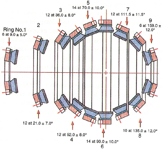
Figure 8.1. Schematic of a vertical section through Microball. The rings of detectors are indicated with their azimuthal angle and the half angle which they subtend. The position of the reaction target is marked with the red cross near the centre. (Reprinted from [1] with the permission of Elsevier.)
Download figure:
Standard image High-resolution image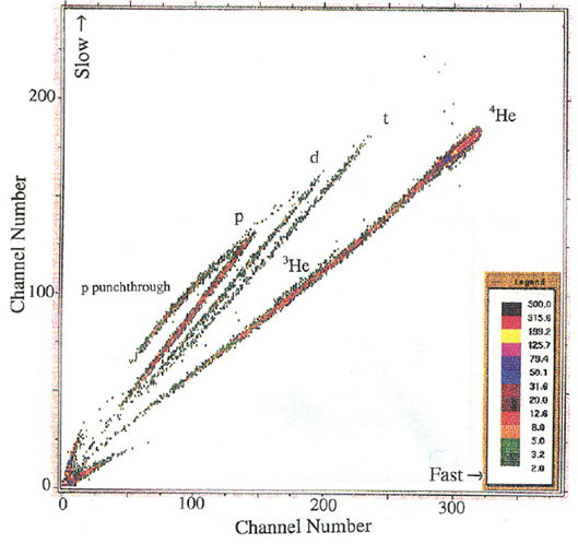
Figure 8.2. Typical charged-particle identification plot for Microball based on plotting the amplitude of the slow component of the CsI(Tl) light output against the fast component. Different loci can be seen corresponding to protons (p), deuterons (d), tritons (t), 3He, and 4He. (Reprinted from [1] with the permission of Elsevier.)
Download figure:
Standard image High-resolution image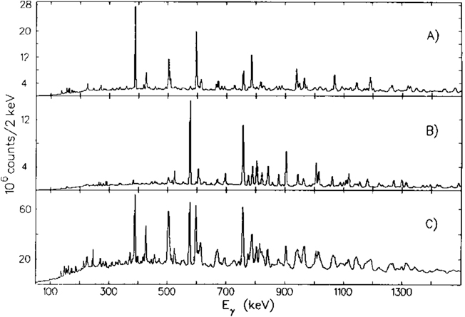
Figure 8.3. Typical gamma ray spectra obtained with the Gammasphere germanium detector array for different charged-particle evaporation channels using Microball. The data is for the fusion-evaporation reaction involving a 130 MeV 28Si beam on a 58Ni target: (a) gamma-ray spectrum selecting the α2p evaporation channel; (b) gamma-ray spectrum selecting the 4p evaporation channel; (c) gamma-ray spectrum without any charged-particle selection. (Reprinted from [1] with the permission of Elsevier.)
Download figure:
Standard image High-resolution imageUoYtube
The UoYtube [2] was constructed for use as a charged-particle veto detector in conjunction with the JUROGAM II germanium detector array at the University of Jyväskylä Finland. The tube consists of 96 CsI(Tl) detectors arranged around six sides of a box with hexagonal cross section (see figure 8.4). The individual detectors comprise a 20 × 20 × 2 mm square tile of CsI(Tl) coupled to an S3590-08 PIN diode from Hamamatsu. Through a digital data acquisition system, pulse shapes can be explored. Figure 8.5 shows the different pulse shapes obtained for protons, alpha particles, gamma rays and piled-up events. Comparing the fast and slow components of the pulses measured, different particle types such as protons and alpha particles can be distinguished (see figure 8.6).
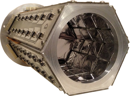
Figure 8.4. The UoYtube comprising 96 CsI(Tl) detectors arranged around six sides of a box with hexagonal cross section. Each detector comprises a 20 × 20 × 2 mm square tile of CsI(Tl) coupled to an S3590-08 PIN diode. (Reprinted from [2] with the permission of IOP Publishing.)
Download figure:
Standard image High-resolution image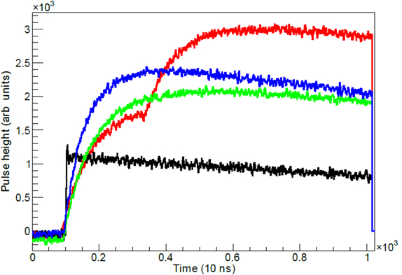
Figure 8.5. Pulse shapes for individual UoYtube detectors for differing particle types: black—a gamma ray; green—a proton; blue—an alpha particle; red—two charged particles in short succession.
Download figure:
Standard image High-resolution image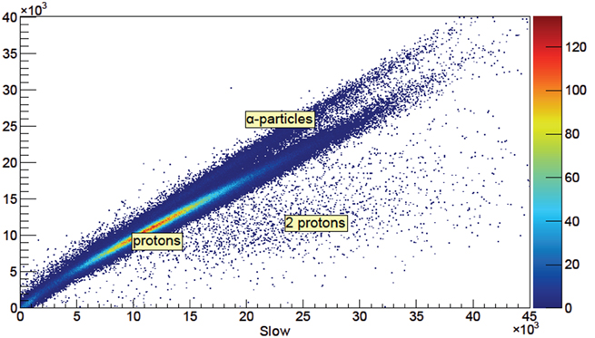
Figure 8.6. The fast signal from the UoYtube
( s) plotted against the slow component
 s). Events due to protons and alpha
particles can be distinguished in the figure.
s). Events due to protons and alpha
particles can be distinguished in the figure.
Download figure:
Standard image High-resolution imageJYtube
In some applications with fusion-evaporation reactions, it is desirable simply to veto any event where a charged particle is detected, e.g. when the interest is in the study of exotic proton-rich nuclei which are populated through in fusion-evaporation reactions by neutron emission only. In this case, the pulse shape discrimination afforded by CsI(Tl) is unnecessary. CsI(Tl) is also intrinsically rather slow due to the slow decay component of the light emitted, meaning that arrays of CsI(Tl) suffer pile-up at high rates. This suggests the possibility of replacing CsI(Tl) with plastic scintillator since the signals from plastic scintillator (see section 9.1.2) are very fast compared with CsI(Tl) and can therefore support high detector rates. The JYtube (see figure 8.7)—a veto detector used at the University of Jyväskylä in Finland, uses plastic scintillator elements coupled to 6 mm × 6 mm SensL J-series silicon photomultipiers (the properties of plastic scintillator are described in section 9.1.2). The modern technology of SiPMs (see section 5.3.3) is more suitable in this application than photodiodes as the SiPMs have a large gain leading to signals which do not need preamplification and can be directly digitised; this dispenses with the preamplification stage required when using photodiodes.

Figure 8.7. The JYtube comprising a similar hexagonal arrangement to the original UoYtube. Each detector comprises a 20 × 20 × 2 mm square tile of plastic scintillator (Eljen EJ-204) coupled to a prism-shaped perspex light guide and joined to a 6 mm square SensL C-series SiPM. The tube comprises two hexagonal halves which join around the reaction target position. Two hexagonal-shaped endcaps (not shown) complete the encirclement of the target. (Photo credit: the author.)
Download figure:
Standard image High-resolution image8.2. Spectroscopy of charged particles: silicon detectors
Silicon detectors are the workhorse of charged particle spectroscopy. In contrast to germanium detectors which can have a significant volume in order to be efficient for gamma-ray detection, silicon detectors are thin, planar, detectors designed to be operated within a vacuum chamber. They provide typical energy resolutions of the order of 30 keV for 5 MeV alpha particles depending on their size and thickness. Elsewhere in this e-book, we have reviewed the basic properties of semiconductors in section 4.3.3 and already described at length, with respect to germanium detectors, many other relevant aspects of semiconductor detectors such as depletion depth (see section 6.2.2). Accordingly, here, we focus on the differences between silicon and germanium, chief of which is silicon's bandgap at room temperature of 1.14 eV compared to 0.67 eV for germanium. The larger bandgap of silicon means that thermal excitation of charge carriers is strongly suppressed compared to germanium meaning that silicon detectors can be operated effectively at room temperature and do not necessarily need to be cooled 1 in the same manner as germanium detectors where it is essential to operate at liquid nitrogen temperatures. This dispenses with the complicated infrastructure needed for the cooling allowing silicon detectors to be mounted in a compact geometry.
8.2.1. Fabrication and design of silicon detectors
The common starting point for silicon detector manufacture is a high-quality silicon wafer, typically 6'' diameter. These wafers are described as detector-grade since they have high-resistivity much exceeding the properties of standard silicon wafers used for other commercial purposes. This high resistivity is important since a key parameter for silicon detectors is the leakage current. Leakage current translates into noise in the detector output and largely originates from thermally generated electron–hole pairs in the material. It scales with the active area of the device meaning that the smallest silicon detectors have the best energy resolution.
The standard 6'' silicon wafer is a size that allows a wide variety of different detector shapes and sizes to be produced (see figure 8.8). The wafers as produced will be either p-type or n-type—as with germanium detectors, this choice can dictate other properties of the material such as its resistance to radiation damage. To turn the wafer into a diode structure requires the introduction of a doping layer, e.g. p+ doping for an n-type wafer near one of the surfaces. This is achieved in industrial clean-room facilities through ion implantation [3] 2 . The wafers are then metallised to provide electrical contacts, diced out of the wafer and mounted on plastic boards with readout tracks and bonding wires are attached. In some cases, replacement of the plastic with ceramic can provide a cleaner system more suitable for ultrahigh vacuum. A grounded guard ring around the perimeter of the detector is usually employed to ensure a uniform electric field distribution [4, 5]. This loses some element of the detector area which may be important when detectors want to be tiled. Accordingly, efforts are under way to produce edgeless detectors with an 'active-edge' [6].

Figure 8.8. Selection of silicon detectors including DSSDs. (Photo credit: the author.)
Download figure:
Standard image High-resolution imageSilicon detectors can be manufactured in thicknesses from 20 μm [7] up to 1 mm or more. The thinnest detectors have a thickness comparable to the range of a typical alpha particle from a sealed source (see figure 8.10) but such detectors are considerably fragile and need caution in their handling. The thicker detectors are more mechanically robust and with thicknesses of around 1 mm, they can also be used for detection of protons, which have longer range than alpha particles of the same energy, and for conversion electrons as well as low energy x-rays and gamma rays. The latter application to conversion electrons will be discussed more extensively in the second part of this chapter (in section 8.4.2).
Even without an applied bias voltage, a silicon detector will have a thin depletion region arising from thermal diffusion of doping ions leading to a small 'in-built' junction potential. The application of a reverse bias will deplete the detector bulk and the depth of the depletion layer may be estimated using equation (6.1) which was discussed earlier in the context of planar germanium detectors. (Strictly speaking a small correction to the reverse bias voltage should be made by adding the small contribution, ∼0.5 V, from the 'in-built' junction potential.) Silicon detectors are usually operated fully depleted. Indeed, the bias voltage often considerably exceeds the voltage for full depletion known as over-depletion in order to improve charge collection, reduce capacitance and, hence, optimise energy resolution. The dependence of the capacitance of the fully-depleted detector on the bias potential, V0, is given by

Choice of a silicon detector for a particular application will depend strongly on the species of charged particles to be detected and their energy. The motivation behind the choice of detector geometry will be discussed more extensively for a range of different applications below.
Some basic silicon detectors suitable for e.g. alpha particle detection are passivated implanted planar silicon (PIPS) detectors; see, for example, the range offered by Mirion. These are conventionally available in a range of thicknesses from 100 to 500 microns, and with a wide range of active areas from 25 mm2 to 5000 mm2. In general, the smaller the sensor, the better the performance due to lower leakage currents. The smallest detectors can offer an alpha particle energy resolution, i.e. for a 241Am source, of 12 keV, while the largest detectors have energy resolutions of order 35 keV.
8.2.2. Identifying charged particles with silicon detectors
Depending on the application, it may be relevant to use silicon detectors not only to make a spectroscopic energy measurement but also to determine the species of the detected charge particle. Historically, this was mostly achieved by constructing detector telescopes with layers of two or more detectors. In recent years, the intrinsic properties of the charge production and collection process in silicon have been harnessed to identify particle species using pulse shape analysis, paralleling many of the developments in pulse shape analysis with large volume germanium detectors (see section 6.5.2). These advances, as with germanium detectors, have been driven by the advent of digital data acquisition. Let us describes these two approaches to identification of charged particle species.
Silicon detector telescopes
The concept behind a detector telescope arises from considerations
of how energy loss
 and range of light charged particles in
silicon differs (see discussion in section 2.2.1). Figure 8.9 shows the strong dependence on
Z, where there is a large difference in
and range of light charged particles in
silicon differs (see discussion in section 2.2.1). Figure 8.9 shows the strong dependence on
Z, where there is a large difference in
 when comparing, for example, protons and
alpha particles for a given energy. In addition, there is a smaller dependence on
isotope where, for example, protons, deuterons
(
when comparing, for example, protons and
alpha particles for a given energy. In addition, there is a smaller dependence on
isotope where, for example, protons, deuterons
( ) and tritons (3H) exhibit
differing energy loss curves. These differences in energy loss are naturally
reflected in differing ranges for charged particles in silicon; figure 8.10 presents the range in
silicon for light ions as a function of their incident energy. It can be seen that a
1 mm thick silicon detector will fully stop alpha particles up to 30 MeV but a 10
MeV proton will 'punch through' meaning that it will exit the detector having not
deposited all its energy. This differing range for particles might be seen as an
inconvenience but it can be exploited to create a detector
telescope which identifies the particle species. A typical telescope
arrangement for charged-particle identification comprises two layers of silicon
detectors: one thin (∼100 μm) and one thick (∼1 mm), where alpha particles will be
fully stopped in the front layer and protons will lose energy in the first layer but
deposit most of their energy in the second layer. While the total energy deposited
in the two detectors may be the same, discrimination between light charged particle
types can be readily obtained by comparing the energy deposited in the front and
back detectors (indeed, often, as in the example just discussed, it may be trivial
as a particle fully stops in the first layer). Examples of silicon detector arrays
that employ the telescope approach are presented in section 8.2.4.
) and tritons (3H) exhibit
differing energy loss curves. These differences in energy loss are naturally
reflected in differing ranges for charged particles in silicon; figure 8.10 presents the range in
silicon for light ions as a function of their incident energy. It can be seen that a
1 mm thick silicon detector will fully stop alpha particles up to 30 MeV but a 10
MeV proton will 'punch through' meaning that it will exit the detector having not
deposited all its energy. This differing range for particles might be seen as an
inconvenience but it can be exploited to create a detector
telescope which identifies the particle species. A typical telescope
arrangement for charged-particle identification comprises two layers of silicon
detectors: one thin (∼100 μm) and one thick (∼1 mm), where alpha particles will be
fully stopped in the front layer and protons will lose energy in the first layer but
deposit most of their energy in the second layer. While the total energy deposited
in the two detectors may be the same, discrimination between light charged particle
types can be readily obtained by comparing the energy deposited in the front and
back detectors (indeed, often, as in the example just discussed, it may be trivial
as a particle fully stops in the first layer). Examples of silicon detector arrays
that employ the telescope approach are presented in section 8.2.4.
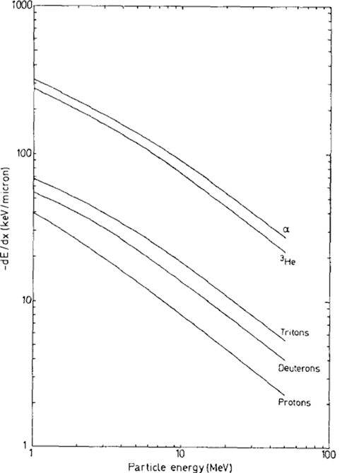
Figure 8.9. Energy loss,
 , of light charged particles in
silicon as a function of particle energy. Energy loss is presented in units of
(keV μm−1). (Reprinted from [8] with the permission of
Elsevier.)
, of light charged particles in
silicon as a function of particle energy. Energy loss is presented in units of
(keV μm−1). (Reprinted from [8] with the permission of
Elsevier.)
Download figure:
Standard image High-resolution image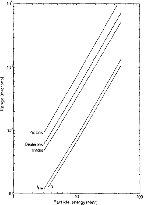
Figure 8.10. Calculated ranges of light charged particles in silicon as a function of particle energy. (Reprinted from [8] with the permission of Elsevier.)
Download figure:
Standard image High-resolution imagePulse shape analysis
Pulse shapes from silicon detectors are found to vary as a function of the energy
and species ( ) of incident ions. This relates to
differences in the depth of penetration, i.e. particle range and the ionisation
density profile, i.e.
) of incident ions. This relates to
differences in the depth of penetration, i.e. particle range and the ionisation
density profile, i.e.
 along the particle track. The effect of
this is subtle in that the ionisation density may be high enough to create plasma
conditions in the semiconductor which creates a time delay in the electron–hole
separation due to a shielding from the bulk electric field in the semiconductor
[9]. Moreover, the
electric field in the semiconductor may be distorted by the highly ionised track
which has a high conductivity with respect to the bulk material. Various strategies
can be applied in terms of the pulse shape analysis. For example, the rise time of
the pulse from the charged-sensitive preamplifier can be used to determine the
particle type for light ions—note the parallel with the employment of rise time in
germanium detectors (see section 6.5.2) for obtaining depth and radius of
the point of interaction—but, here, the information obtained is different. Figure
8.11 provides an
example of such an analysis, plotting the rise time against the energy of particles
to discriminate isotopes up to A = 12 [10]. In this example, rise time is
defined as the time for the signal to rise from 20% to 80% of the full height. A
parallel approach is to investigate the maximum of the current signal from the
detector, achieved by differentiating the output of the charge sensitive
preamplifier prior to digitisation. Figure 8.12 shows an implementation of this
approach with a test experiment using the ISO-FAZIA system (see reference [11] for full details).
Separation of charged particles by Z is achieved up to
Z = 36 and isotopic separation is also possible for particles
with
along the particle track. The effect of
this is subtle in that the ionisation density may be high enough to create plasma
conditions in the semiconductor which creates a time delay in the electron–hole
separation due to a shielding from the bulk electric field in the semiconductor
[9]. Moreover, the
electric field in the semiconductor may be distorted by the highly ionised track
which has a high conductivity with respect to the bulk material. Various strategies
can be applied in terms of the pulse shape analysis. For example, the rise time of
the pulse from the charged-sensitive preamplifier can be used to determine the
particle type for light ions—note the parallel with the employment of rise time in
germanium detectors (see section 6.5.2) for obtaining depth and radius of
the point of interaction—but, here, the information obtained is different. Figure
8.11 provides an
example of such an analysis, plotting the rise time against the energy of particles
to discriminate isotopes up to A = 12 [10]. In this example, rise time is
defined as the time for the signal to rise from 20% to 80% of the full height. A
parallel approach is to investigate the maximum of the current signal from the
detector, achieved by differentiating the output of the charge sensitive
preamplifier prior to digitisation. Figure 8.12 shows an implementation of this
approach with a test experiment using the ISO-FAZIA system (see reference [11] for full details).
Separation of charged particles by Z is achieved up to
Z = 36 and isotopic separation is also possible for particles
with  .
.

Figure 8.11. Rise time versus detected particle energy for different reaction products from the 12C+27Al reaction at 63 MeV. Bands corresponding to different particle types are marked. (Reprinted from [10] with the permission of Elsevier.)
Download figure:
Standard image High-resolution image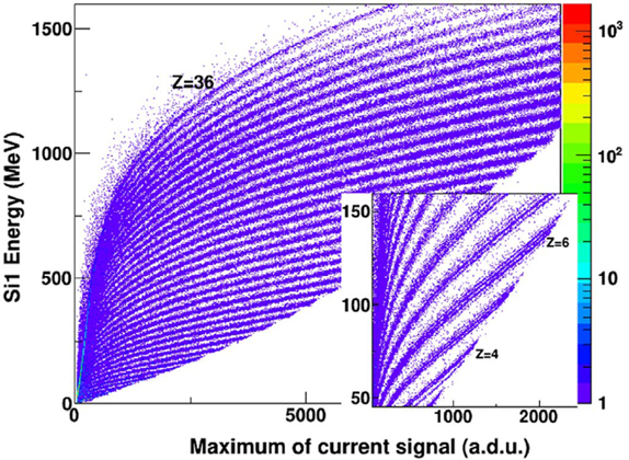
Figure 8.12. Energy recorded in the silicon detector against the maximum of the current signal, obtained from pulse-shape analysis. The experiment used a 80Kr beam at 35 MeV/u incident on a 40Ca target, hence, fragments up to Z = 36, corresponding to Krypton, are observed. Isotopic separation is observed up to Z = 20; the inset shows the isotopic separation at low Z. (Reprinted from [11] with the permission of Elsevier.)
Download figure:
Standard image High-resolution image8.2.3. Obtaining position sensitivity within silicon detectors
In chapter 3, we outlined some topical examples of studies in experimental nuclear physics such as Coulomb excitation (section 3.4.5) and single-particle transfer reactions (section 3.4.6) where it is important to detect both light and heavy ions with high position (or angular) resolution. Some classes of silicon detector are able to provide this functionality: the older-generation of position-sensitive detectors which use resistive strip technology, and more modern double-side silicon strip detectors (DSSDs). We will outline the functionality of these two different classes of detectors below along with examples of where they are used.
Position sensitive detectors
A position sensitive detector (PSD) is an older detector design intended to provide information on the position of interaction [12–14]. The operating principle behind some different designs of PSD is shown in figure 8.13. The most common design for a two-dimensional PSD is to have a resistive electrode and read out signals from contacts on the four corners. The position sensitivity is derived from the ratio of the signals on the four corners by means of resistive charge division. The cathode on the reverse can be standard and then be used to read out a signal with good energy resolution. The chief drawback of such detectors is that the position and energy calibration is significantly more complex than with double-sided silicon strip detectors, which are discussed in section 8.2.4 below; this is because there is no intrinsic pixellation. The standard technique is to apply a mask with small regularly spaced holes in it in order to characterise the position sensitivity using a source. Position distortion occurs due to the ballistic deficit effect [15]; reconstruction of the distorted signal is discussed in [16].

Figure 8.13. Two designs of position sensitive detectors (PSDs): (a) pin-cushion PSD where the front side is a resistive sheet; the signals are taken at the four metallised contacts located on the corners and are used to determine the position. The back side is a metallic contact film used to improve the energy resolution. Without the resistive strip, Rl, the spatial resolution is high but the spatial linearity is very poor. With a resistive strip the response is quite linear while the spatial resolution is degraded; (b) a duo-lateral PSD where both sides are resistive with contacts located at the four edges on both sides (and orthogonally); this kind of PSD offers both a quite good spatial resolution and a good spatial linearity; but the drawback of this detector is the poor energy resolution. (Reprinted from [13] with the permission of Elsevier.)
Download figure:
Standard image High-resolution imageFigure 8.14 shows an example of a linear array of position-sensitive silicon detectors used as part of the HELIOS spectrometer. The array is used to detect light charged particles following single-particle transfer reactions within the bore of a solenoidal magnet. The particles follow helical trajectories before striking the linear silicon array; this application was discussed in section 3.4.6.
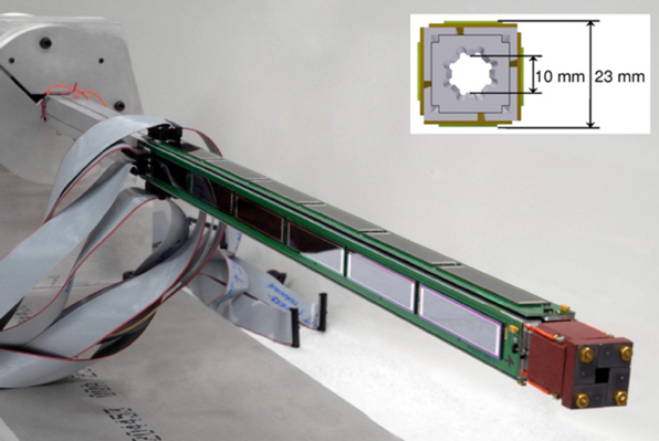
Figure 8.14. Silicon detector array for the HELIOS spectrometer at Argonne National Laboratory. Each detector is position sensitive and has an active area of 9 × 50.5 mm. The inset is a cross-section of the array. (Reprinted from [17] with the permission of Elsevier.)
Download figure:
Standard image High-resolution image8.2.4. Double-sided silicon strip detectors
A significant advance in development of silicon detectors from the point of view of
nuclear physics was the advent of double-sided silicon strip detectors (DSSDs) [18]. The silicon is divided
into strips on each side using passivated strips in between typically comprising
SiO2 of about 0.1 mm width. This can be applied either to a rectangular
detector achieving  strips or to an annular detector where it
is divided on one side into rings and the other side into sectors. The dimensions of
these strips/rings/sectors can be tuned according to the application of interest.
There are several manufacturers of such detectors; the widest range of detector
geometries is offered by Micron
Semiconductor Ltd.
strips or to an annular detector where it
is divided on one side into rings and the other side into sectors. The dimensions of
these strips/rings/sectors can be tuned according to the application of interest.
There are several manufacturers of such detectors; the widest range of detector
geometries is offered by Micron
Semiconductor Ltd.
The division of the silicon detector into strips provides effective pixelisation of the detector which is exploited in the subsequent data analysis, where following appropriate calibration of the strips, events detected in strips on the two sides can be associated by requiring that they correspond in energy within a certain tolerance set according to the experimental conditions and the relevant energy resolution. Not all events can be reconstructed in such a fashion because there is non-negligible probability that an incident particle hits the passivated region between strips. When this happens, two effects can occur: (1) electron trapping so incomplete charge collection results and (2) charge sharing where the charge is collected on two adjacent strips [19]. These two effects are shown in figure 8.15. These design-related features need careful handling in the subsequent data analysis and some events are inevitably discarded reducing efficiency.

Figure 8.15. Illustration of the effects introduced by inter-strip passivation on a DSSD illuminated by a 241Am source (left) incomplete charge collection within a single strip leading to a low energy tail on an alpha peak (right) charge sharing shown by plotting the apparent energy recorded in two adjacent strips. (Reprinted from [19] with the permission of IOP Publishing.)
Download figure:
Standard image High-resolution imageImplantation detectors
DSSD detectors are commonly used for implantation at the focal plane of a recoil spectrometer; such a spectrometer separates fusion residues from scattered beam using a combination of electric and magnetic fields; this application was briefly introduced in section 3.3.1. The benefit of a silicon detector in this application is that it can record both the implantation of the recoiling nucleus and its subsequent decay, if the decay is via emission of a particle with a short range, e.g. an alpha particle. The intrinsic segmentation of the DSSD into effective pixels allows implantation and subsequent decay to be correlated so long as the decay process is fast relative to the implantation rate per pixel. This technique is known as recoil-decay tagging (RDT). Typically in RDT studies, the heavy ion implanted has a relatively low energy. Given that the energy loss for such a heavy ion is high in silicon compared to light ions such as protons and alpha particles, the heavy ion will implant close to the front surface of the silicon detector. This short range is much less than the thickness of any practical silicon detector. The thickness of the detector used can vary and this is dictated by the characteristics of the subsequent decay of interest:
- Where the decay concerns emission of an alpha particle or proton then a thin detector will be optimal as the thinner the detector, the better the achievable energy resolution. Typical thicknesses employed are in the range 150–700 μm. In some cases involving heavy nuclei, the alpha emission will reach excited states in the daughter nucleus which then decay by emission of conversion electrons. Since both the alpha particle and electrons are emitted from the same implanted atom within the silicon detector, the energy deposited by the alpha particle and the conversion electron may effectively sum which is a feature that needs to be taken account of in the analysis [20].
- Where the decay concerns emission of a beta particle, energy resolution is of no importance because beta particles follow a broad distribution of energies—the Fermi–Kurie distribution (as described in section 1.4). Here, the identification of the beta particle emission is important as a means of correlating events. However, beta particles deposit much less energy in a given range of silicon than alpha particles. In this case, DSSDs with thicknesses up to 1 mm are more suitable so that energy loss by the beta particle is higher in order to identify beta particles above the noise.
An example of an implantation system is the GREAT spectrometer [21] at the University of Jyväskylä which is designed for implantation and decay studies. Two rectangular DSSDs are mounted side by side and cover the focal plane of the RITU recoil separator (see figure 8.16). The photograph also shows a planar germanium detector (see section 6.4.1) which is installed behind the DSSDs and can record low-energy gamma rays or x-rays, as well as beta particles.
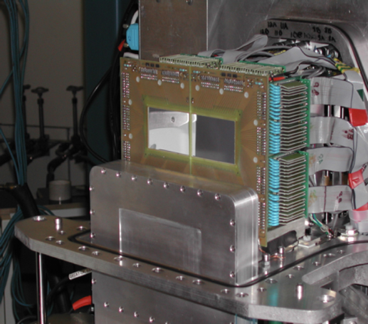
Figure 8.16. Focal plane of the GREAT spectrometer at University of Jyväskylä. The planar germanium detector is lowered to show the two DSSDs. (Photo credit: the author.)
Download figure:
Standard image High-resolution imageScintillator alternatives to silicon implantation detectors
As an aside, it is worth mentioning innovations using scintillators as replacements to DSSDs (and other applications where silicon detectors are used). Scintillators lack the high energy resolution of silicon detectors but they have a number of advantages such as being radiation hard, and dependent on the scintillator they can have very fast time response allowing fast counting. A good example of a replacement scintillator is YAP:Ce [22, 23] which is a material readily produced in thin sheets—a common application for it is as an electron or x-ray screen. YAP:Ce has a fast decay time of 28 ns. This makes it possible to resolve two successive events within 100 ns of each other. This has initially been applied to a specialist application of searching for two fast successive alpha decays following implantation of a recoiling heavy ion [24]. Figure 8.17 provides a schematic of a novel implantation detector based on YAP:Ce; the system can achieve sub-mm position resolution in x and y which is comparable to that of a silicon-based DSSD [24].

Figure 8.17. YAP:Ce scintillator detector for implantation studies. The YAP:Ce crystal is a monolithic slab with 50.8 mm diameter and a thickness of 1 mm. The scintillation light enters a segmented, quartz, light guide with 24 × 24 pixels, and falls on to a Hamamatsu position-sensitive photomultiplier tube (PSPMT) with 64 segments. (Reprinted with permission from [24]. Copyright (2019) by the American Physical Society.)
Download figure:
Standard image High-resolution imageAnnular detectors
Annular detectors are an elegant design for nuclear physics experiments with accelerated beams [25]. With the beam directed down the centre of the hole in the annular detector, the rings will subtend the same angle with respect to the beam direction. An example of such an annular detector is the S3 pattern from Micron Semiconductor Ltd which is shown in figure 8.18. The S3 detector is electrically segmented into 24 rings on the junctions side and 32 sectors (wedges) on the ohmic side. Data is usually collected independently for the two sides of the detector and can be reassociated in the offline analysis to determine more precisely the point of interaction from requiring that the energy for an event recorded on the two sides matches. An exception to this is in the case of charge sharing where the interaction took place at the point of the electrical segmentation and charge is recorded in the two adjoining annular rings or wedges.
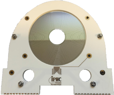
Figure 8.18. Micron S3 detector mounted on a ceramic mount. (Photo credit: the author.)
Download figure:
Standard image High-resolution imageExamples of silicon detector arrays for transfer reaction studies
Silicon detector arrays are ideal for nuclear reaction studies such as
single-particle transfer reactions (see section 3.4.6) where they are often combined
with an array of high-purity germanium detectors. This technique is increasingly
being applied to studies with radioactive beams in inverse kinematics, meaning a
high-Z beam on a low-Z target, e.g. deuterated
plastic target. Reviews of this topic and the relevant methodologies are given in
references [26] and
[27]. Annular
silicon detectors are very suitable for this application based on their geometry
which provides good angular resolution. Measurement of particles as a function of
angle with respect to the beam direction is critical to this application. Figure
8.19 illustrates the
kinematics of typical light-ion transfer reactions in inverse kinematics; most light
ion ejectiles are detected at small angles (up to
 ) where
 is the beam direction. A large portion of
this angular range can be readily covered with an annular silicon detector (or
detector telescope) at forward angles. Moreover, such annular detectors have a hole
in the middle, allowing the beam to pass through the silicon detector.
is the beam direction. A large portion of
this angular range can be readily covered with an annular silicon detector (or
detector telescope) at forward angles. Moreover, such annular detectors have a hole
in the middle, allowing the beam to pass through the silicon detector.
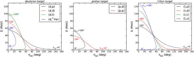
Figure 8.19. Kinematics of various transfer reactions for a 54Ca beam at 10 MeV/u
impinging on a light ion target: deuteron (left), proton (centre) and triton
(right). The kinematics are shown as a function of lab angle, each locus has the
centre-of-mass angle labelled at the two ends:
 and
and
 . (Reprinted from [27] with the
permission of IOP Publishing.)
. (Reprinted from [27] with the
permission of IOP Publishing.)
Download figure:
Standard image High-resolution imageAnnular silicon detectors can be used to identify which excited states are produced in the transfer reaction and the probability of excitation as a function of angle from the measured intensity of light charged particles, e.g. protons, deuterons, alpha particles detected in the various annular rings. In practice, the achievable energy resolution for the charged particles is limited by the properties of the accelerated radioactive beams employed and the parameters on the targets used since these often need to be thick to maximise the number of reactions observed with low intensity radioactive beams. Such arrays of annular silicon detectors are therefore commonly coupled with high-purity germanium detectors (see chapter 6) or other scintillator-based gamma-ray detectors with good intrinsic energy resolution, e.g. LaBr3(Ce) detectors (see section 5.2.1). The germanium detectors record γ rays emitted from the excited states populated in the reaction. Selecting coincidences between these characteristic gamma rays and the light charged particles can be used to separate the different reaction channels and effectively recover the energy resolution for charged particles. There are several such systems in operation worldwide; some examples include TIARA [28], SHARC [29] and CAKE [30]. Here, we focus in more detail on a specific example, the STELLA array [31].
STELLA
STELLA [31] is a dedicated station built to measure the 12C+12C fusion reaction which is one of the key processes governing the evolution of massive stars [32]. STELLA is designed to measure evaporated charged particles, i.e. protons and alpha particles in coincidence with gamma rays from excited states. A 3D CAD drawing of STELLA is presented in figure 8.20. The evaporated charged particles are measured with three annular silicon strip detectors: two of Micron S3 design and one of Micron S1 design (see figure 8.21). One S1 and S3 form a telescope to discriminate protons from alpha particles. STELLA has been coupled to the FATIMA LaBr3(Ce) array described in section 5.4.2. This has offered yet another means of discriminating between light ions such as protons and alpha particles using the excellent, fast rise time properties of the LaBr3(Ce) detectors as a time reference. Figure 8.22 shows the energy of light charged particles detected from 12C+12C fusion as a function of the time difference between the detection of a coincident gamma ray with FATIMA and a charged particle in the annular silicon DSSD. Two loci are observed—one corresponding to protons and one to alpha particles; the separation achieved is because of the differing rise time in the silicon detector of the proton and alpha particle-induced events. It is worth emphasising that it is the sub-ns timing resolution of the LaBr3(Ce) detectors that makes this possible. Large germanium detectors have too poor a timing resolution to allow this approach to be applied.
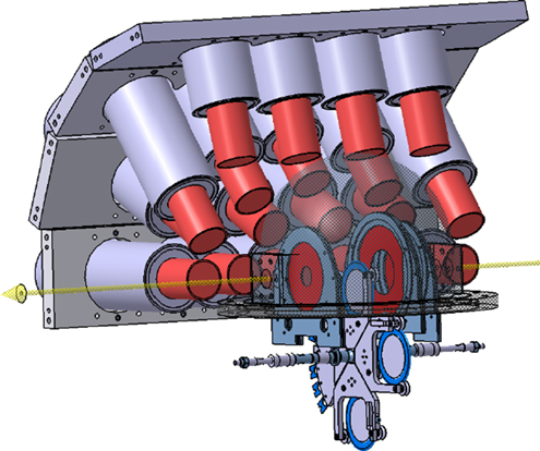
Figure 8.20. 3D-rendered CAD drawing of STELLA. The volume of the scattering chamber is shown semi-transparent in order to allow its interior to be viewed, comprising three annular silicon detectors, and a target holding/rotating mechanism. The large circular carbon target foils are shown with blue frames on their perimeter. The direction of the 12C beam (from right to left in the diagram) is shown with the yellow arrow. Only half of the LaBr3(Ce) gamma-ray array is depicted for clarity of presentation.
Download figure:
Standard image High-resolution image
Figure 8.21. Annular silicon detectors: 2 off Micron S3 and one Micron S1 (the larger area detector in the centre) mounted inside the reaction chamber of STELLA. (Photo credit: the author.)
Download figure:
Standard image High-resolution image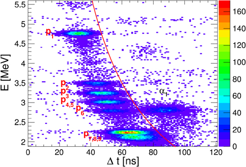
Figure 8.22. Distinguishing evaporated protons and alpha particles using time difference between the silicon signal and LaBr3(Ce) array in STELLA. (Reprinted from [31] with the permission of Elsevier.)
Download figure:
Standard image High-resolution image8.2.5. Specialist applications of silicon detectors—storage rings
Nuclear physicists are increasingly exploring the potential of storage rings for nuclear reactions studies [33]. Here, highly-charged, high energy ion beams circulate in a ring and can initiate scattering or transfer reactions with, e.g. light nuclei in a gas-jet target. Storage rings operate in ultrahigh vacuum (UHV) conditions, i.e. with a pressure below 10−10 mbar. A conventional silicon detector would be unsuitable for such conditions as they are generally manufactured on a plastic frame. The plastic would outgas spoiling the UHV conditions and the detector could not be baked. Specialist DSSD detectors have been developed for the ESR storage ring at GSI [34]. These detectors are on a specialist ceramic mount so they can be baked. They form an effective window between the UHV of the storage ring and an auxiliary (lower quality) vacuum in a pocket behind them where further detectors such as thick Si(Li) detectors can be mounted to form a detector telescope (see figure 8.23).
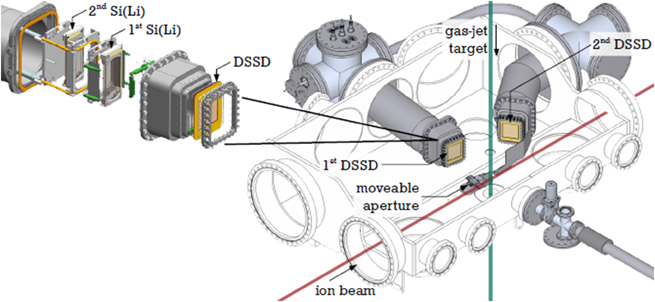
Figure 8.23. Design of DSSD telescopes to detect reactions in a storage ring. (Reprinted from [34] with the permission of IOP Publishing.)
Download figure:
Standard image High-resolution image8.2.6. Operation and calibration of silicon detectors
Having reviewed the basic physics of silicon detectors and some of their many variants and applications, it is appropriate to say something more specific about how to operate them and achieve the best performance. Firstly, a suitable, low-noise, regulated bias supply will be needed which is capable of handling the necessary voltage and currents. The bias voltage required depends on the silicon detector in use but is of order 10–500 V. Ideally, the supply should have the capability of reading out leakage current to high precision since this is one of the key operating parameters and a major shift in leakage current is one of the first indications that there is a problem. It's important to note, that if the silicon detector is not in a temperature-stabilised environment then a diurnal cycle will be commonly seen in the leakage current due to the change in ambient temperature over the course of the day and night. This is normal and should be monitored during operation. The bias supply should also have the capacity to ramp up the bias voltage slowly and ramp off the voltage should there be a power outage although this is not such a big concern as it is for germanium detectors which operate on much higher voltage. A suitable low-noise preamplifier will also be required. Preamplifers are also available in high density units with 16–64 channels of input which is advantageous for DSSDs commonly employed in experimental nuclear physics. Preamplifier output can then go to a suitable shaping amplifier and then to an MCA, or directly to a digitiser unit. There are several options on the market for relevant NIM (or other standard) electronics. In nuclear physics, a commonly-found electronics platform for silicon detectors is that supplied by Mesytec who offer, for example, a four-channel bias supply with high precision current readout, the MHV-4, and high-density preamplifiers, e.g. the MPR-16.
Basic setup of a silicon detector
Testing of a silicon detector will commonly take place in a vacuum chamber using an alpha source; alpha particles lose energy in air and so a good vacuum is required to minimise such energy loss. A silicon detector is conventionally supplied with details on its depletion voltage and an I–V curve which plots the leakage current as a function of applied bias. It is a common source of misconception and so worth explaining clearly here that the situation with regard to biasing the detector is rather different to that for a germanium detector. With a germanium detector, a recommended bias voltage is provided and operating above this voltage will be risky. Silicon detectors can often be safely operated significantly above the nominal depletion voltage (sometimes two or three times higher than the nominal value) and their performance can continue to increase as charge collection becomes more rapid in the increased electric field. The key is to monitor the leakage current and observe that it is following the expected diode response. A further difference to germanium detectors is that most silicon detectors will operate at some level even with no bias applied due to the 'built-in' bias potential and the thin depletion region setup by it, albeit with very poor energy resolution.
A first step would be to verify the supplied I–V curve while monitoring the output signal on an oscilloscope, increasing the bias voltage in small steps to allow the system to settle. This should verify that the detector is performing according to specification. Energy calibration of a silicon detector is conventionally carried out with a triple-alpha source (see section 3.1.1) to ensure linearity. In the same procedure, the energy resolution can be determined from fitting the peak widths. Given that each of the three main alpha peaks has a small satellite peak below it, being able to resolve these satellites visually in a histogram immediately implies the energy resolution is good. There are some subtleties to energy calibration of silicon detectors that must be borne in mind. Firstly, silicon detectors frequently have a dead layer (SiO2) and metallisation, e.g. aluminium on their surfaces. An alpha particle from a source loses energy continuously along its track and so will already have lost some energy before it enters the active volume of the silicon detector. This needs to be corrected for otherwise there would be a discrepancy in the suggested energy of alpha particles emitted from a heavy ion implanted into a DSSD, for example. Such energy losses can be calculated and removed from the calibration using, e.g. SRIM (see section 2.2.8). A second important effect is that the pulse height in a silicon detector generated by a charged ion of a given energy differs depending on the ion species [35]. It has been suggested that this relates to the energy required to generate an electron–hole pair in silicon which depends on the charge of the ion (see figure 8.24). The correction is not particularly large—of order 1% between protons and alpha particles. However, such a correction needs to be applied if, for example, a silicon detector is calibrated, as is usual, with an alpha particle source and then latterly used to measure protons.
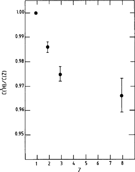
Figure 8.24. Apparent electron–hole pair creation energy ratios for 4He, 7Li and 16O relative to 1H as a function of atomic number, Z. (Reprinted from [35] with the permission of Elsevier.)
Download figure:
Standard image High-resolution imageDetector damage
Silicon detectors suffer from radiation damage after being exposed to a high fluence of charged particles, leading to them often being considered a consumable item in experimental nuclear physics. Radiation damage of a silicon detector will lead to decreased pulse height and degradation of energy resolution which continues to the point where the detector is no longer useful for spectroscopic measurements. Damage effects are most severe in a flux of heavy ions [36] and are signalled by a strong (and irreversible) increase in leakage current. There are other ways in which leakage current can increase which are unrelated to damage. For example, if the detector has been insufficiently grounded then it can become charged up in an in-beam experiment by the spray of delta electrons from the target which can appear to greatly increase the leakage current. This leakage current will disappear if the detector is turned off and allowed to recover.
Radiation damage in silicon is associated with the generation of Frenkel defects in the crystal which act as charge-trapping centres leading to electron–hole recombination. For DSSDs, damage to the interstrip region can lower its resistance leading to incomplete charge collection and cross-talk between strips [36]. One of the issues with radiation damage is that it can be highly localised, particularly if the flux of particles is high in a specific angular range, for example. Nevertheless, even if the damage is local, it can spoil the properties of the detector as a whole. There are strategies which can mitigate radiation damage; an example applied to an annular DSSD is discussed in reference [37]. The left-hand side of figure 8.25 shows the impact of radiation damage on an annular DSSD. In each case, the pulse height is plotted for alpha source events in a given sector (or ring) as a function of ring (or sector) on the other side of the DSSD. Since the damage is localised in the inner rings (high ring number), the pulse height is significantly degraded for events registering in the inner rings. The approach taken to remedy this was to consider the DSSD as a large number of pixels based on each ring/sector combination and apply an algorithm to correct the pulse height on a pixel by pixel basis. This largely recovers the resolution of the DSSD as shown on the right-hand side of figure 8.25.

Figure 8.25. Pulse heights from triple-alpha source recorded by radiation damaged DSSD: (a) events across the set of 32 rings correlated with an event recorded in sector 17. (b) The same events corrected on a pixel-basis (see text for details). (c) Events recorded across the 64 sectors correlated with an event recorded in ring 20. (d) The same events corrected on a pixel-basis (see text for details). (Reprinted from [37] with the permission of Elsevier.)
Download figure:
Standard image High-resolution image8.2.7. Alternatives to silicon
Diamond and silicon carbide detectors
Diamond detectors have been used to a minor extent in nuclear physics [38]. They are more widely
employed in high-energy particle physics, principally as beam monitors. At very high
energies, e.g. for
 protons, the radiation hardness of
diamond detectors can be ten times higher. However, diamond detectors can suffer
radiation damage more easily than silicon detectors at low energies—the more typical
domain of nuclear physics [39, 40].
Silicon carbide detectors have also been discussed as a radiation-hard alternative
to conventional silicon [41].
protons, the radiation hardness of
diamond detectors can be ten times higher. However, diamond detectors can suffer
radiation damage more easily than silicon detectors at low energies—the more typical
domain of nuclear physics [39, 40].
Silicon carbide detectors have also been discussed as a radiation-hard alternative
to conventional silicon [41].
Optical time-projection chamber
In the examples discussed above, we have seen the routes to spectroscopic measurements of alpha particles and heavy ions and how position sensitivity can be used to infer the angle of emission of particles in nuclear reaction studies. Here, we discuss a fascinating example of where it is possible to 'image', albeit indirectly, the tracks of alpha particles (and other heavy ions) in a gas volume. This can be important for study of break-up reactions where, for example, a high energy photon beam interacts with 16O and breaks it up into 12C + 4He [42]. The three-dimensional imaging is achieved with an Optical Readout Time Projection Chamber (O-TPC) (see figure 8.26). Within the gas volume, ionisation occurs and electrons drift, through a Frisch grid, into an amplification volume. The resulting electron avalanches and ionisation generate optical photons which can be imaged using CCD cameras leading to a two-dimensional projection. The third dimension is obtained from the projected time-structure recorded by photomultiplier tubes (PMTs). Figure 8.27 shows an example of the image reconstruction of 12C dissociated into three alpha particles using the O-TPC.
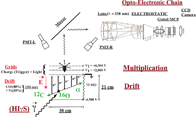
Figure 8.26. A schematic diagram of the O-TPC with an 16O target nucleus dissociated by a gamma-ray beam from the HIγS facility. The gas mixture and pressure as well as the operating voltages are indicated. The drift electrons that provide the third (time projection) upward dimension are shown schematically. (Reprinted from [42] with the permission of IOP Publishing.)
Download figure:
Standard image High-resolution image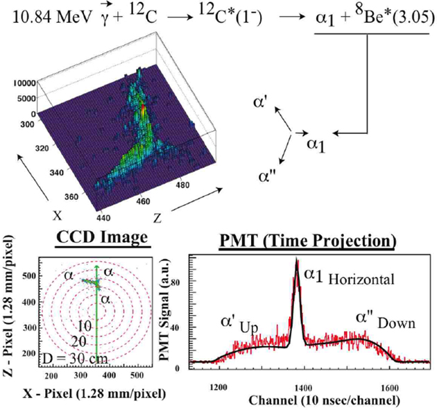
Figure 8.27. Three alpha-particle event from the dissociation of 12C measured at
100 Torr. The projected 2D track and time of this event are shown in the lower
part of the figure together with the fitted line shape of the light detected
from the emerging three alpha particles. The geometry of the reconstructed event
is shown schematically with
 emitted horizontally and the
8Be decay products,
emitted horizontally and the
8Be decay products,
 and
and
 , emitted upward and downward,
respectively. (Reprinted from [42] with the permission of IOP
Publishing.)
, emitted upward and downward,
respectively. (Reprinted from [42] with the permission of IOP
Publishing.)
Download figure:
Standard image High-resolution image8.3. Applications relevant to fission
Studies of fission are motivated by a focus on our fundamental understanding of nuclear fission as well as applications to conventional nuclear fission energy generation and to fission of exotic short-lived nuclei relevant to nucleosynthesis. The underlying physics of the fission process was reviewed in section 1.5. From this perspective, it is of high interest to understand the cross-sections for neutron-induced fission which can be achieved by simply counting the number of fission events. A secondary objective would be to determine the fragment species, i.e. Z and A so that the fission mechanism can be understood in detail. Let us first look at basic system for fission counting before moving to more elaborate apparatus which allow the fission fragment mass distribution to be obtained and finally systems which can also identify the Z of fission fragments.
8.3.1. Counting fission events
In order to obtain cross sections for neutron-induced fission, a simple counter is
needed for fission events with high efficiency. At the nToF facility in CERN (see
section 3.5.1), the
MicroMegas detector [43] is used. Figure 8.28 shows a schematic of the MicroMegas detector. The sample, in this case,
235U is mounted directly inside the chamber. Neutrons interact with the
235U inducing fission. The geometry ensures a very high probability that
one of the fission fragments will enter the gas volume; such a heavy charged ion will
create significant ionisation of the fill gas. The electrons will drift slowly towards
the anode, and ions towards the cathode. The key feature of the detector design is a
micro-mesh situated close to the anode which separates the drift region from a narrow
amplification region with high electric field where electron multiplication will
occur. The micromesh enables a high gain
( ) and fast timing. Such a detector can also
be used to register light charged particles from, e.g. (n,α) and
(n,p) reactions.
) and fast timing. Such a detector can also
be used to register light charged particles from, e.g. (n,α) and
(n,p) reactions.
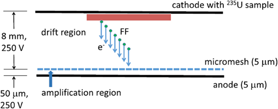
Figure 8.28. Schematic setup of a MicroMegas detector used at nToF. These detectors are
defined by two gas volumes: the drift region, typically a few mm in thickness, and
the amplification region, a few tens of microns thick. These regions are separated
by a micro-mesh layer of a few microns. Electrons produced by the charged
particles emitted from the sample are drifting to the mesh and are triggering an
avalanche signal in the high electric field of
 cm−1 of the amplification
region. (Reprinted from [44] with the permission of Elsevier.)
cm−1 of the amplification
region. (Reprinted from [44] with the permission of Elsevier.)
Download figure:
Standard image High-resolution image8.3.2. Identifying the fission fragment mass distribution
There is a wide variety of apparatus used for fission studies, tuned to the needs of the specific experimental study since a wide range of experimental techniques are employed where accelerated ion beams or fast/thermal neutrons are used in producing a fissioning system [45]. The parameters of interest in such studies are principally the kinetic energies and velocities of the fission fragments and their angle with respect to the beam direction. An ideal detector would therefore have excellent angular resolution, energy resolution and timing resolution. Timing resolution is important because it allows time-of-flight of fragments to be measured and hence the velocity of fission fragments to be reconstructed. All available detectors naturally have some limitations against these idealised requirements. For example, the timing resolution of silicon detectors is not particularly good, which provides a limitation to time-of-flight measurements. They also suffer from pulse-height defect when detecting heavy ions, which depends on the mass and charge of the ions. Moreover, as discussed above, silicon detectors are not especially radiation hard and so their performance can noticeably degrade. These considerations mean that gas-ionisation based detectors are often preferable for fission studies given their high rate capability, intrinsically fast timing and relative radiation hardness. Many of these considerations are applicable to detection of heavy ions in other experimental settings not involving fission.
Fission fragment detection with silicon detectors: beta-delayed fission
An application where fission fragment detection with silicon detectors is appropriate is in the study of beta-delayed fission where low fission event rates are expected and so radiation damage is not of high concern [46]. Figure 8.29 illustrates such an implementation where silicon detectors are used for fission fragment detection. A low-energy radioactive beam of 180Tl, at the very low rate of 150 atoms s−1, is implanted into thin carbon foils on a 'windmill' system which rotates stepwise. 180Tl beta decays to 180Hg. A small fraction of this decay branch goes to highly excited states which spontaneously fission. The fission fragments are detected in two annular silicon detectors mounted either side of the implantation foil. MINIBALL germanium cluster detectors are mounted behind one of the silicon detectors to measure coincident gamma rays. The system allows the measurement of the individual and total fission fragment kinetic energies which affords insight into the mass asymmetry in the fissioning system.

Figure 8.29. Detector set ups for study of β-delayed fission. (Left) a 'windmill' setup where a radioactive beam of 180Tl is implanted at low energy into thin carbon foils on a windmill which can be rotated. (Right) a blow-up of the left. (Reprinted with permission from [46]. Copyright (2010) by the American Physical Society.)
Download figure:
Standard image High-resolution imageFission fragment detection with MWPCs
Figure 8.30 shows a setup for measuring fission fragments following a multi-nucleon transfer (MNT) reaction where a number of nucleons are transferred onto a heavy system such as 238U to produce a heavier, excited nucleus which then fissions. Information on the number of nucleons transferred can be measured using an array of silicon ΔE–E telescopes (see section 8.2.2) to identify the beam-like residual nucleus and, hence, the fissioning system. The fission fragments are recorded in four multi-wire proportional counters (MWPCs). MWPCs [47] are a well-established variant of the proportional counter discussed in section 4.3.1. The gas-filled proportional counter contains a crossed array of anode wires. When the fission fragment enters the MWPC volume, it causes ionisation and the charges are collected on the neighbouring wires. This provides information on the position of interaction within the gas volume. MWPCs generate a fast timing signal (∼1 ns) which supports time-of-flight measurements 3 and high rate capability; they are also intrinsically radiation hard.

Figure 8.30. A typical detection setup for in-beam MNT-induced fission experiments at JAEA. In the case shown, the MNT reaction 18O+238U was studied, whereby four MWPCs: MWPC-A–MWPC-D were used to detect the coincident fission fragments, while a silicon ΔE–E telescope array was exploited to determine the transfer channel. In the case of the fusion–fission experiments, the ΔE–E telescope array is removed. (Reprinted from [45] with the permission of IOP Publishing.)
Download figure:
Standard image High-resolution image8.3.3. Determining both A and Z of fission fragments
A key challenge for fission fragment spectrometry and other areas of experimental
nuclear physics is to determine the Z of heavy ions. In section 2.2.1, we discussed the
physics of stopping of heavy charged particles in matter, in particular the
Bethe–Bloch formula (equation (2.1)) which shows an explicit dependence on the
atomic number of the particles. We also discussed the appearance of the characteristic
Bragg peak at the end of a heavy ion track as the energy loss increases strongly at
low velocities. This property can be exploited using a Bragg curve spectrometer [48]; a schematic of such a
spectrometer is shown in figure 8.31. The spectrometer comprises an ionisation chamber with a Frisch grid
close to the anode. The heavy ion loses energy and stops within the ion chamber
volume. The current signal from the ion chamber represents a time inverse of the
stopping process. The ionisation from the end of the track appears first, followed by
the rest of the track moving backwards in time. The two key points in the signal are
the position of the Bragg peak and the initial energy loss
 as shown on figure 8.31. This technique works best for ions
with higher energies, e.g. few MeV/u; separation of Z becomes
challenging for
as shown on figure 8.31. This technique works best for ions
with higher energies, e.g. few MeV/u; separation of Z becomes
challenging for  .
.

Figure 8.31. Concept of a Bragg curve spectrometer comprising an ionisation chamber with a Frisch grid close to the anode. The current signal shows a time-reversed profile of the track of ionisation.
Download figure:
Standard image High-resolution imageThis technology is applicable to fission fragment detection but, here, the situation is more complex as the fragments have typical kinetic energies of 1 MeV/u. At such energies, the ion may not be fully ionised and charge exchange can occur with the fill gas in an ionisation chamber. This variation in the effective charge states of the ions serves to 'wash out' the Bragg peak. Figure 8.32 shows examples of this effect from fragments of the same Z and different mass, and for close-lying isotopes of different Z. The identification of fission fragments by Z becomes, therefore, very challenging but not impossible.

Figure 8.32. Profiles of simulated average energy loss with range in 100 mbar of isobutane by
fragments with kinetic energy-to-mass ratios of 1 MeV/u. Panel (a) shows energy
loss by  Kr fragments illustrating the effect
mass has on stopping. Panel (b) shows 90Kr, 95Sr and
100Zr energy loss, demonstrating differences in energy loss with
change in atomic number and mass for typical 235U fission fragments.
The profiles were simulated and averaged over 20 fragments of each type using
SRIM-2013. (Reprinted from [49] with the permission of Elsevier
under Creative Commons License.)
Kr fragments illustrating the effect
mass has on stopping. Panel (b) shows 90Kr, 95Sr and
100Zr energy loss, demonstrating differences in energy loss with
change in atomic number and mass for typical 235U fission fragments.
The profiles were simulated and averaged over 20 fragments of each type using
SRIM-2013. (Reprinted from [49] with the permission of Elsevier
under Creative Commons License.)
Download figure:
Standard image High-resolution imageLet us describe a system which employs a Bragg detector and other detectors to
determine fission fragment Z and A. The FiFI
spectrometer, designed by the University of Manchester, is an example of a
![$2E2\mathit{\unicode[Book Antiqua]{x76}}$](https://content.cld.iop.org/books/10__1088_978-0-7503-1428-2/revision2/bk978-0-7503-1428-2ch8ieqn29.gif) (two energy—2 velocity) spectrometer where
there are two detector arms which measure the kinetic energy and velocity of the
fission fragments. Since, the fission fragments are travelling at non-relativistic
velocities, their kinetic energy, Ek
is
connected to their velocity by the conventional formula
(two energy—2 velocity) spectrometer where
there are two detector arms which measure the kinetic energy and velocity of the
fission fragments. Since, the fission fragments are travelling at non-relativistic
velocities, their kinetic energy, Ek
is
connected to their velocity by the conventional formula

This provides a route to identifying their atomic mass, A, if their kinetic energy and velocity can be measured with sufficient precision. Indeed, if the masses of the two fragments, A1 and A2 could be determined with high enough precision then the number of neutrons emitted in the fission process could also be established event-by-event; this, however, is significantly challenging.
Each of the two arms of the FiFI spectrometer comprise a set of detectors: a START
detector, a Bragg detector volume (similar to the example described above) and a STOP
detector (see figure 8.33) [49].
The START and STOP detector are used to determine the time-of-flight of fission
fragments through the spectrometer arm with high precision. When fission fragments
pass through these detectors, electrons are emitted from a thin foil of aluminium (10
± 1 μg cm−2 thick), called a secondary electron emission (SEE) foil, held
at a −1.75 kV potential. Backscattered electrons enter the space between the foil and
the electrostatic mirror, which consists of two wire grids separated by 1 cm. A
potential of −3.5 kV is applied across the gap between the grids in order to deflect
the electrons into the microchannel plate (MCP) assembly. The two MCPs are
 mm-thick lead-doped glassplates with
 μm-wide tubular channels, which extend from
one side of the plate to the other at an angle to the surface. A voltage of −4.8 kV is
applied across the MCPs, accelerating the electrons which enter it in order to cause
ejection of secondary electrons in the collisions with the walls. The collisions in
the MCPs multiply the number of electrons by a factor of
μm-wide tubular channels, which extend from
one side of the plate to the other at an angle to the surface. A voltage of −4.8 kV is
applied across the MCPs, accelerating the electrons which enter it in order to cause
ejection of secondary electrons in the collisions with the walls. The collisions in
the MCPs multiply the number of electrons by a factor of
 106. The timing resolution of the
time-of-flight component of FIFI is around 1.2 ns.
106. The timing resolution of the
time-of-flight component of FIFI is around 1.2 ns.
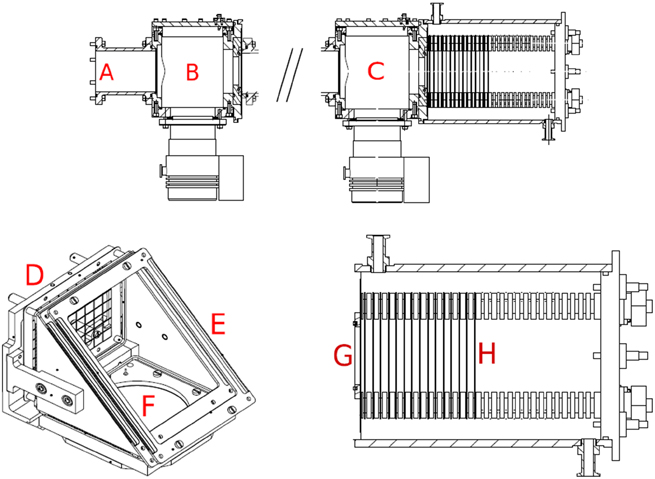
Figure 8.33. A schematic diagram of the fission fragment identification arm. The entry point of a FF beam is marked with letter A. Letters B and C denote volumes where the START and STOP detector assemblies are positioned. The positions of the vacuum pumps are shown beneath those volumes. The 1 m-long ToF section has been truncated for the purposes of the diagram. An expanded view of the timing detectors is shown in the bottom left part of the diagram. Letter D marks the location where the mesh supporting the emission foil is located. Letter E denotes the plane onto which the electrostatic mirror is attached. The MCP is located at letter F. Note that the timing detector in the diagram is shown upside down compared to its actual orientation inside FiFI. An expanded view of the BD is shown in the bottom right corner. The mylar window is at letter G, followed by a gas-filled volume containing the field-shaping rings, the Frisch grid and an anode (position H). ToF foils were removed during data collection for the results presented in this work. (Reprinted from [49] with the permission of Elsevier under Creative Commons License.)
Download figure:
Standard image High-resolution image8.3.4. Societal applications of alpha particle/heavy-ion detection
There are relatively fewer societal applications of charged-particle detection such as alpha-particle detection compared to the broad range of applications of gamma-ray detection discussed in chapter 7. Alpha spectrometry is relevant to nuclear, environmental and biological samples; a recent review of these applications is found in reference [50]. Silicon detectors such as PIPS detectors are frequently used in such applications. Here, we look at two specific applications of heavy charged particle detection relevant to nuclear decommissioning and space science.
Decommissioning of pipework at nuclear installations
The decommissioning of nuclear sites requires reliable techniques for the detection, identification, and quantification of radioactive substances. Discriminating between disposable and contaminated waste has a significant impact on the cost of decommissioning. In particular, there is no simple, low-cost solution available for assessing the presence of radioactive sources that are essentially alpha-only emitters, such as 239Pu, on the inner walls of pipework. The range of alpha particles in media is intrinsically short, and as such, alpha-emitters are undetectable from the outside, as any radiation occurring on the inside of the pipe is absorbed by the wall (even gamma radiation from 235U excited states). The emitting isotope may even be embedded in tiny cracks in the pipe wall, meaning that alpha particles may lose energy as they emerge. Consequently, alpha-particle detectors need to be positioned as closely as possible to the inner walls in order to achieve the greatest detection efficiency and be able to detect very low radiation doses.
A detector system has been developed [51] based on flexible crystalline silicon that can conform to the inner diameter of pipework for the direct detection of alpha-particles. This solution not only offers the potential for 360° inner diameter coverage but can also be adapted to pipes of different diameters. Being as close as possible to the inner pipe walls, maximum sensitivity and uniform efficiency can be achieved, even for low energy alpha-particles, where other approaches may struggle. As a proof-of-principle, it was demonstrated that a sheet of flexible crystalline silicon of 50 μm thickness, as shown in figure 8.34, forms the basis for a high-performance in-pipe alpha-particle detector (see figure 8.35). The sensor can be more generally adapted to any curved surface, such as the exterior of barrels filled with radioactive waste. It can also address the requirements of some nuclear physics experiments that require non-planar detectors.

Figure 8.34. At thicknesses of about 50 μm, silicon becomes flexible and can be bent into cylindrical or other curved geometries. (Reprinted from [51] with the permission of AIP Publishing under Creative Commons License.)
Download figure:
Standard image High-resolution image
Figure 8.35. A curved silicon detector (50 μm) thick designed for use as a pipeline inspection system for alpha-contamination. (Photo credit: the author.)
Download figure:
Standard image High-resolution imageCosmic ray telescope
In section 7.6, we
described aspects of gamma-ray astronomy and the strong synergies between the
techniques of experimental nuclear physics, in particular the application of
high-purity germanium detectors and anti-coincidence shields. Here, we describe an
example relating to charged-particle detection in the area of Space Science where
the techniques and technology employed also have strong connections with nuclear
physics. The example is the Low-Energy Telescope (LET) which is one of four
sensors that make up the Solar Energetic Particle (SEP) instrument of the IMPACT investigation for NASA's STEREO mission [52] (figure 8.36). The LET is designed to measure the
elemental composition, energy spectra, angular distributions, and arrival times of
charged particles from the Sun: protons and helium ions over the energy range
∼1.5–13 MeV/u and heavier ions up to nickel over the energy range from ∼2 to ∼30
MeV/u. This is a very similar energy range to that encountered in low energy nuclear
physics although the directionality of the particles is clearly different. The
detection and identification of ions with LET is achieved with an array of silicon
detector telescopes (see section 8.2.2). The detectors making up the
telescopes, L1–L3, have differing thicknesses: L1 detectors are 24 μm thick, L2 are
50 μm thick and L3 are 1000 μm thick. The principle here is the same as in the
nuclear physics example: an ion with incident energy, E, will
transit one (or more) of the thin detectors and deposit an energy
 in a thickness, L. In
the case where the particle is not normally incident to the detector surface,
L can be adjusted to take account of the angle of incidence. The
stopping detector records the residual energy,
in a thickness, L. In
the case where the particle is not normally incident to the detector surface,
L can be adjusted to take account of the angle of incidence. The
stopping detector records the residual energy,
 , where
 . The particle's corresponding atomic
number, Z, can be obtained from [52]
. The particle's corresponding atomic
number, Z, can be obtained from [52]

where
 is the mass to charge ratio of the nuclei
under consideration and k and a are constants
which model the range-energy relationship for heavy ions in silicon (see section
2.2.1). Figure
8.37 shows Monte
Carlo simulations of the energy deposited in the different elements of the detector
telescopes which shows interesting parallels with some of the nuclear physics
examples discussed above. The readout of the LET system illustrates interesting
aspects of digital electronics. There are 54 individual silicon elements. These are
readout by custom-made Pulse Height Analysis System Integrated Circuits
(PHASICs)—see discussion of ASICs in section 10.3. A Minimum
Instruction Set Computer (MISC) automatically translates these measured energies
into particle identification for ∼12 energy intervals at event rates around 1000
events s−1 [52].
is the mass to charge ratio of the nuclei
under consideration and k and a are constants
which model the range-energy relationship for heavy ions in silicon (see section
2.2.1). Figure
8.37 shows Monte
Carlo simulations of the energy deposited in the different elements of the detector
telescopes which shows interesting parallels with some of the nuclear physics
examples discussed above. The readout of the LET system illustrates interesting
aspects of digital electronics. There are 54 individual silicon elements. These are
readout by custom-made Pulse Height Analysis System Integrated Circuits
(PHASICs)—see discussion of ASICs in section 10.3. A Minimum
Instruction Set Computer (MISC) automatically translates these measured energies
into particle identification for ∼12 energy intervals at event rates around 1000
events s−1 [52].

Figure 8.36. Schematic of the Low-Energy Telescope (LET), part of the STEREO-IMPACT mission. (a) Arrangement of silicon detector telescopes within the LET; (b) the shape and dimensions of the three telescope elements, L1, L2 and L3. Dimensions are in mm. The L1 detectors are 24 μm thick, L2 are 50 μm thick and L3 are 1000 μm thick. (Reprinted by permission from Springer: [52].)
Download figure:
Standard image High-resolution image
Figure 8.37. Monte Carlo simulations of the response of the LET system to particles incident on the A side (see figure 8.36). (Left) plots of energy deposited in L1A and L2A detectors, and L2A and L3A detectors marked with the ion species. (Right) the same Monte Carlo data but corrected for the angle of incidence. The simulations include variation in the L1 detector thickness, Bohr/Landau fluctuations in particle energy losses, and electronic noise contributions. (Reprinted by permission from Springer: [52].)
Download figure:
Standard image High-resolution image8.4.
 and electron detection

8.4.1. Beta decay spectroscopy
As discussed in section 1.4, β spectra are largely uninteresting from a spectroscopic point of view since beta decay is a three-body decay and the energy distribution of beta particles is continuous up to the end-point. The location of the end-point is of interest, however, since it can be used to determine the mass difference between parent and daughter nuclei. In contemporary studies of exotic nuclei, relatively few ions are produced of a given exotic nucleus and it is desirable to measure the beta decay half life and learn about the details of the decay in terms of which daughter states are populated in the decay observed through their subsequent gamma-ray emission. This often requires a detector which can detect implantation of high energy heavy ions and then detect their beta decay. These successive events can be correlated via their position. Let us discuss three systems that can provide this functionality, observing how they draw on a diverse set of detector technologies.
DSSD-stack implantation detector
The first example is a stack of nine DSSDs (Micron Model W1-1000) used at RIKEN-RIBF in Japan, where each DSSD was segmented into 16 strips in the horizontal and vertical axes as a position-sensitive β-counting system (see figure 8.38). Incoming heavy ions are degraded in energy and then implanted into one of the DSSDs in the stack. The subsequent beta decay can be correlated with the implantation by detecting the beta particle in the same DSSD pixel. The beta particle will not be fully stopped in the DSSD but will lose energy as it passes through the DSSD and where that energy exceeds the threshold set on the detector it can be registered as a beta particle. Depending on the implantation depth of the heavy ion within the DSSD, the efficiency for β particle detection varies from 40% to 80% [53].
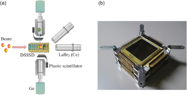
Figure 8.38. Apparatus for correlating beta decay of radioactive nuclei used at RIBF-RIKEN in 2009: (a) incoming high energy radioactive ions are stopped in a stack of double-sided silicon-strip detectors (DSSD) and then subsequently beta decay; the position of implantation and decay can be correlated. γ rays are detected by four Compton-suppressed clover-type Ge detectors arranged around the DSSDs in a close geometry. (b) Photograph of the stack of nine DSSDs. (Reprinted from [53] with permission from OUP under Creative Commons License.)
Download figure:
Standard image High-resolution imageYSO-based implantation detector
An alternative concept uses a scintillator-based, pixellated implantation-decay
detector constructed from the inorganic scintillator, YSO. Figure 8.39 provides a schematic
of such a device [54]. YSO is chosen for its high effective atomic number (Z
= 35) and density (4.4 g cm−3) which can stop beta particles in a
relatively short range. YSO is radiation hard and so will not be damaged as rapidly
as a more conventional silicon implantation detector. Moreover, it can support high
counting rates due to its fast decay time (42 ns). In the example shown, the YSO is
pixellated into sticks of
 .
.

Figure 8.39. (Left) schematic of a YSO-based beta-implant detector. (Right) photograph of the detector. (Reprinted from [54] with the permission of Elsevier.)
Download figure:
Standard image High-resolution imageCAITEN revolving pixellated plastic scintillator system
The third example to be discussed (see figure 8.40) is an innovative design using a
rotating highly-pixellated cylindrical array of plastic scintillators
4
called CAITEN which has also been used at RIKEN-RIBF in Japan [53]. There are 40 000
pixels of plastic scintillator each with dimensions of
 mm3. Energetic radioactive
ions are implanted into a region of the detector. The detector is rotating at a rate
between 0 and 60 rpm to reduce the density of non-correlated decay events in a given
pixel; this is the same philosophy as that behind earlier tape-transport systems
where radioactive ions are stopped on a tape and transported to detectors where the
decay is subsequently observed. The scintillation light is recorded with a
cylindrical array of 24 position-sensitive photomultiplier tubes (PSPMTs). Each
PSPMT has a segmented light guide mounted in front of it. The light is transported
across an air gap of around 3–4 mm between the scintillator barrel and the light
guides.
mm3. Energetic radioactive
ions are implanted into a region of the detector. The detector is rotating at a rate
between 0 and 60 rpm to reduce the density of non-correlated decay events in a given
pixel; this is the same philosophy as that behind earlier tape-transport systems
where radioactive ions are stopped on a tape and transported to detectors where the
decay is subsequently observed. The scintillation light is recorded with a
cylindrical array of 24 position-sensitive photomultiplier tubes (PSPMTs). Each
PSPMT has a segmented light guide mounted in front of it. The light is transported
across an air gap of around 3–4 mm between the scintillator barrel and the light
guides.
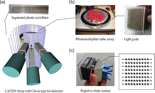
Figure 8.40. CAITEN beta-counting system (see text for more detailed description): (a) segmented plastic scintillators. (b) Position-sensitive photomultiplier tube array. (c) Resistive channel readout of the PSPMTs. (Reprinted from [53] with permission from OUP under Creative Commons License.)
Download figure:
Standard image High-resolution image8.4.2. Conversion electron spectroscopy
Conversion electron spectroscopy (see section 1.7.3) is more interesting from a spectroscopic perspective than beta decay because the peaks are discrete and have different components, i.e. K, L etc, whose relative intensity is an indicator of the multipolarity of the transition concerned (see section 1.7.3). Lithium-drifted silicon (or Si(Li)) detectors [55] are often used for electron detection since the addition of lithium allows the depletion layer to be much deeper and hence, the detector to have a depth more appropriate to the range of electrons. Figure 8.41 shows a conversion electron spectrum from a 207Bi source acquired with a 6.5 mm thick Si(Li) detector. The achievable energy resolution corresponds to 0.77 keV at 481 keV which is sufficient even to resolve the separate L1, L2, etc components.

Figure 8.41. (Left) conversion electron spectrum from a 207Bi source using a 6.5 mm
thick Si(Li) detector. The inset shows the K, L,
 peaks corresponding to conversion
electrons for the 570 keV transition. (Right) beta decay spectra for the
144Ce–144Pr decay. (Reprinted from [56] with the permission of IOP
Publishing.)
peaks corresponding to conversion
electrons for the 570 keV transition. (Right) beta decay spectra for the
144Ce–144Pr decay. (Reprinted from [56] with the permission of IOP
Publishing.)
Download figure:
Standard image High-resolution imageWhile thick Si(Li) detectors are suitable for measurement of conversion electrons following beta decay, detection of conversion electrons is more challenging in in-beam experiments, e.g. fusion-evaporation as described in section 3.3.1, principally due to the fact that an accelerated ion beam striking a reaction target produces a flood of delta electrons which would swamp a silicon detector mounted near the target position. The SACRED spectrometer [57] built at the University of Jyväskylä in the 1990s has design features to avoid these issues. Electrons are transported away from the target using a solenoidal field. They pass through a high voltage barrier which can repel the lower energy delta electrons allowing the higher energy conversion electrons to pass through. The conversion electrons are detected in a 5 × 5 array of 5 mm square PIN diodes. The array is cooled to around −20 °C to strongly reduce the leakage current in the PIN diodes. A typical conversion electron spectrum obtained with SACRED in an in-beam study is shown in figure 8.42. Clearly, K and L components of different transitions can be resolved but the energy resolution is much lower than that of the Si(Li) spectrum shown in figure 8.41 which is partially due to the intrinsic resolution of the detectors but also attributable to Doppler-broadening of the peaks as this data is from an in-beam experiment (see further discussion of this effect in section 3.3.1).
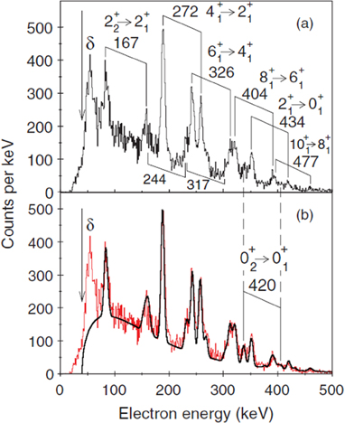
Figure 8.42. Conversion electron spectrum for 180Hg measured with SACRED. (top) The K and L peaks are marked for various transitions. (bottom) A simulation of the data. (Reprinted with permission from [58]. Copyright (2011) by the American Physical Society.)
Download figure:
Standard image High-resolution imageSPEDE [59] is an example of a next-generation electron spectrometer designed for Coloumb excitation studies, specifically for high-Z nuclei where internal conversion is an important process (see section 3.4.5). It comprises an annular silicon detector, segmented into 24 segments: 3 rings and 8 sectors (see figure 8.43). Variants can be produced with variable thickness up to 1.5 mm depending on the energy range of interest for the conversion electron study; a typical thickness is 500 microns. The preamplifiers are mounted directly on the circuit board around the silicon detector and surface-mount field effect transistors (FETs). The circuit board and silicon detector sit on a copper cooling block allowing the system to be cooled to around 5 °C for improved operation with lower leakage currents. Delta electrons are handled in this case by biasing the target holder up to +5 kV.
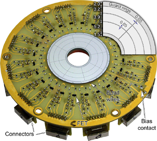
Figure 8.43. The SPEDE spectrometer—an annular silicon DSSD for conversion electron measurements in-beam. (Reprinted by permission from Springer Nature [59].)
Download figure:
Standard image High-resolution imageElectron-gamma ray coincidence detection
Since many experimental studies populate highly excited nuclear states which emit many coincident gamma rays (and conversion electrons in competition with gamma ray emission), there is high interest in detecting gamma ray-conversion electron coincidences particularly for studies of high-Z nuclei where the probability for conversion electron emission is significantly higher (see section 1.7.3). The SAGE spectrometer [60, 61] is an evolution of the earlier SACRED design (see above) and uniquely allows coincident detection of gamma rays and conversion electrons in in-beam studies. Figure 8.44 shows the design of how the electron spectrometer component of SAGE interfaces with a germanium detector array while figure 8.45 shows an expanded view of the electron spectrometer itself. A societal example of electron-gamma ray coincident detection for measuring atmospheric Radioxenon was already provided in section 7.3.
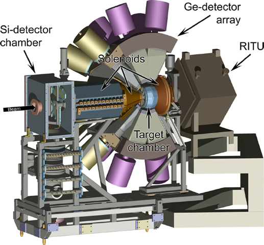
Figure 8.44. The SAGE spectrometer—a unique spectrometer for simultaneous conversion electron/gamma-ray detection. (Reprinted by permission from Springer Nature [60].)
Download figure:
Standard image High-resolution image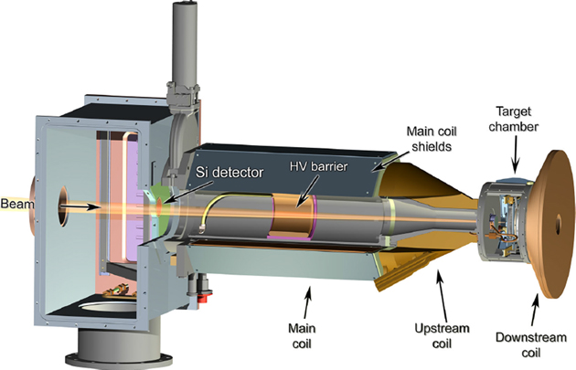
Figure 8.45. The electron spectrometer part of SAGE. (Reprinted by permission from Springer Nature [60].)
Download figure:
Standard image High-resolution image8.4.3. Pair spectrometer
Internal pair conversion, as discussed in section 1.7.3, is only a subject of interest for
transitions exceeding 1.022 MeV. Given that most transitions in heavier nuclei are
below this energy threshold, it makes internal-pair spectrometry a somewhat specialist
application focussed on light nuclei. It is of high interest to measure the angular
correlation between the emitted electron and positron since this contains information
of the multipolarity of the transition. Figure 8.46 provides an illustration of the design
of such a pair spectrometer which has six detector modules, each comprising a
plastic-scintillator
 telescope which can distinguish high energy
electrons or positrons from gamma rays [62]. In order to achieve good angular
resolution each
telescope which can distinguish high energy
electrons or positrons from gamma rays [62]. In order to achieve good angular
resolution each
 telescope has a position-sensitive,
multi-wire proportional counter (MWPC) in front of it. The efficiency of such a
coincidence detector system is relatively low, of order 1% (see bottom of figure 8.46) which makes such
studies very challenging.
telescope has a position-sensitive,
multi-wire proportional counter (MWPC) in front of it. The efficiency of such a
coincidence detector system is relatively low, of order 1% (see bottom of figure 8.46) which makes such
studies very challenging.
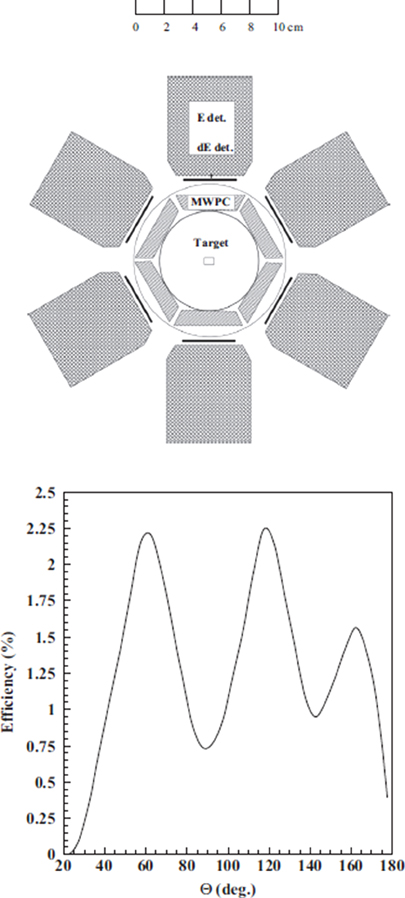
Figure 8.46. (top) Design of a coincidence pair spectrometer with high angular resolution.
There are six detector modules, each with an MWPC for position sensitivity backed
up by a
 telescope of plastic scintillator.
(bottom) The efficiency of the pair spectrometer as a function of the opening
angle of the emitted positron–electron pair. (Reprinted from [62] with the permission
of Elsevier.)
telescope of plastic scintillator.
(bottom) The efficiency of the pair spectrometer as a function of the opening
angle of the emitted positron–electron pair. (Reprinted from [62] with the permission
of Elsevier.)
Download figure:
Standard image High-resolution imageAn alternate system for pair spectrometry is the Super-e spectrometer at the Australian National University (ANU) [63] (see figure 8.47). Positron–electron pairs are produced at the target position following a nuclear reaction. The positrons and electrons are transported in helical trajectories in a magnetic field to an array of thick, segmented Si(Li) detectors which detect both electrons and positrons. Baffles placed within the spectrometer can be moved to select the 'energy bite' in terms of which electrons/positrons are transported.
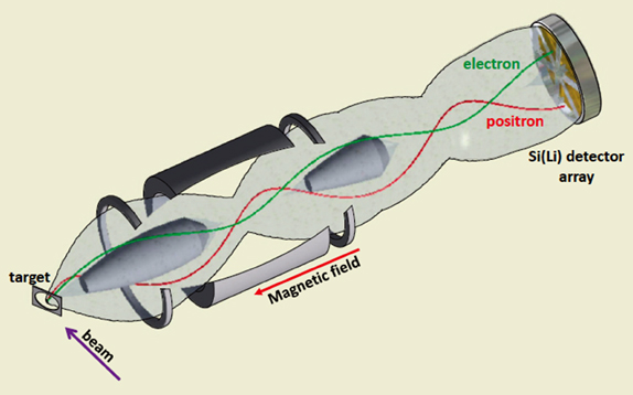
Figure 8.47. Schematic of the Super-e magnetic pair spectrometer comprising a superconducting solenoid, baffles and an array of thick Si(Li) detectors. (Reprinted from [63] with the permission of EDP Sciences under Creative Commons License.)
Download figure:
Standard image High-resolution image8.4.4. Societal applications of beta detection
PET isotope assay
Radioisotopes for positron emission tomography (PET) are produced at cyclotron
facilities and subsequently prepared as various molecules in solution such as
18F-FDG. A standard task in the assay of such materials is to establish
their activity and their purity. Measurements of activity are conventionally based
on detection of annihilation photons (511 keV) following the
 decay of the radioisotope by positron
emission. This is carried out using a standard gamma-ray detector, e.g. based on a
NaI(Tl) scintillator. There is increasing interest in the PET community in
'dose-on-demand' systems where single doses of a specific radiotracer would be
produced on site when required. Allied to this is the desire to miniaturise the
apparatus involved in handling the radiotracer using microfluidic chips. Recent
advances in photodetector technology such as SiPMs offer a route to a compact
detector which can directly detect the positrons emitted from the radiotracer [64, 65]. Figure 8.48 shows a prototype detector system
based on plastic scintillator (see section 9.1.2) with a thickness of 1 mm and a 6
mm square Sensl C-series SiPM (see section 5.3.3). At this thickness, the
background from 511 keV annihilation photons is negligible as the probability for
gamma rays to interact with plastic scintillator is very low (the main mode of
interaction for plastic scintillator is Compton scattering). This system has been
tested by injecting a plug of radiotracer solution sequentially through a
conventional NaI(Tl) annihilation gamma-ray detection system and then into the
microfluidic chip with its integrated positron detector. Figure 8.49 shows that both detector systems are
capable of recording the radiotracer activity.
decay of the radioisotope by positron
emission. This is carried out using a standard gamma-ray detector, e.g. based on a
NaI(Tl) scintillator. There is increasing interest in the PET community in
'dose-on-demand' systems where single doses of a specific radiotracer would be
produced on site when required. Allied to this is the desire to miniaturise the
apparatus involved in handling the radiotracer using microfluidic chips. Recent
advances in photodetector technology such as SiPMs offer a route to a compact
detector which can directly detect the positrons emitted from the radiotracer [64, 65]. Figure 8.48 shows a prototype detector system
based on plastic scintillator (see section 9.1.2) with a thickness of 1 mm and a 6
mm square Sensl C-series SiPM (see section 5.3.3). At this thickness, the
background from 511 keV annihilation photons is negligible as the probability for
gamma rays to interact with plastic scintillator is very low (the main mode of
interaction for plastic scintillator is Compton scattering). This system has been
tested by injecting a plug of radiotracer solution sequentially through a
conventional NaI(Tl) annihilation gamma-ray detection system and then into the
microfluidic chip with its integrated positron detector. Figure 8.49 shows that both detector systems are
capable of recording the radiotracer activity.

Figure 8.48. A micro-fluidic chip-based detector for PET isotope assay. (a) Top-down design of the chip. (b) Side view showing PMMA element with microfluidic channel, plastic scintillator and SiPM. (c) Photographs of the assembled chip detectors. (Reprinted from [64] with permission from University of York.)
Download figure:
Standard image High-resolution image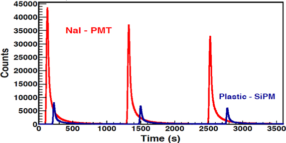
Figure 8.49. A plug of 10
 18F-PDG in solution (157 MBq ml−1) is injected
sequentially through a system comprising a NaI(Tl) gamma ray detector with lead
shielding, and a microfluidic chip with integrated plastic scintillator detector
coupled to SiPM. (Reprinted from [64] with permission of University of
York.)
18F-PDG in solution (157 MBq ml−1) is injected
sequentially through a system comprising a NaI(Tl) gamma ray detector with lead
shielding, and a microfluidic chip with integrated plastic scintillator detector
coupled to SiPM. (Reprinted from [64] with permission of University of
York.)
Download figure:
Standard image High-resolution imageNuclear decommissioning
As discussed in section 3.1.2, 90Sr is a common beta-only emitter used as a radioactive
source. This radioisotope is commonly found in nuclear decommissioning sites as it
is a long-lived isotope
( years) produced in nuclear fission [66]. Leaks and spills of
material can lead to it being found in groundwater at nuclear installations.
Conventionally, in order to assess such contamination, samples of water are
obtained, manipulated and processed in a laboratory. It would be highly advantageous
to have a direct in situ measurement. Figure 8.50 shows a concept of an in
situ detector using a gallium arsenide (GaAs) PIN diode [66]. GaAs has a large
bandgap (1.42 eV) meaning that it can operate at room temperature without suffering
appreciably from thermal noise; it is also a radiation-hard material.
years) produced in nuclear fission [66]. Leaks and spills of
material can lead to it being found in groundwater at nuclear installations.
Conventionally, in order to assess such contamination, samples of water are
obtained, manipulated and processed in a laboratory. It would be highly advantageous
to have a direct in situ measurement. Figure 8.50 shows a concept of an in
situ detector using a gallium arsenide (GaAs) PIN diode [66]. GaAs has a large
bandgap (1.42 eV) meaning that it can operate at room temperature without suffering
appreciably from thermal noise; it is also a radiation-hard material.

Figure 8.50. Concept for a groundwater beta detector based on an in situ GaAs photodiode. (Reprinted from [66] with the permission of Elsevier.)
Download figure:
Standard image High-resolution image
References
- [1]Sarantites D G, Hua P-F, Devlin M, Sobotka L G, Elson J, Hood J T, LaFosse D R, Sarantites J E and Maier M R 1996 'The Microball' Design, instrumentation and response characteristics of a 4π-multidetector exit channel-selection device for spectrocopic and reaction mechanism studies with Gammasphere Nucl. Instrum. Methods A 381 418–32
- [2]Henderson J et al 2013 Enhancing the sensitivity of recoil-beta tagging J. Instrum. 8 04025
- [3]Hyder A 1981 Ion-implanted and bakeable silicon detectors Nucl. Instrum. Methods 187 595–8
- [4]Beck G A et al 1997 Radiation-tolerant breakdown protection of silicon detectors using multiple floating guard rings Nucl. Instrum. Methods A 396 214–27
- [5]Evensen L, Hanneborg A, Avset B and Nese M 1993 Guard ring design for high voltage operation of silicon detectors Nucl. Instrum. Methods A 337 44–52
- [6]Koybasi O et al 2020 Edgeless silicon sensors fabricated without support wafer Nucl. Instrum. Methods A 953 163176
- [7]Valtonen E et al 2016 Fabrication of a thin silicon detector with excellent thickness uniformity Nucl. Instrum. Methods A 810 27–31
- [8]Skyrme D J 1967 The passage of charged particles through silicon Nuclear Instrum. Methods 57 61–73
- [9]Tove P A and Seibt W 1966 Plasma effects in semiconductor detectors Nucl. Instrum. Methods 51 261–9
- [10]Mahata K et al 2018 Particle identification using digital pulse shape discrimination in a nTD silicon detector with a 1 GHz sampling digitizer Nucl. Instrum. Methods A 894 20–4
- [11]Pastore G et al 2017 Isotopic identification using Pulse Shape Analysis of current signals from silicon detectors: Recent results from the FAZIA collaboration Nucl. Instrum. Methods A 860 42–50
- [12]Laegsgaard E 1979 Position-sensitive semiconductor detectors Nucl. Instrum. Methods 162 93–111
- [13]Solal M C 2007 The origin of duo-lateral position-sensitive detector distortions Nucl. Instrum. Methods A 572 1047–55
- [14]Banu A et al 2008 Performance evaluation of position-sensitive silicon detectors with four-corner readout Nucl. Instrum. Methods A 593 399–406
- [15]Qiao R, Li J, Wang J, Dai X and Le Y L 2012 Charge collection and equalization for position-sensitive silicon strip detector Nucl. Instrum. Methods A 686 38–42
- [16]Cowin R L and Watson D L 1997 Surface charge flow in two-dimensional position sensitive silicon detectors Nucl. Instrum. Methods A 399 365–81
- [17]Lighthall J C et al 2010 Commissioning of the HELIOS spectrometer Nucl. Instrum. Methods A 622 97–106
- [18]Davinson T 2004 Multistrip silicon detectors for studies with low energy RNBs Nucl. Phys. A 746 188c–94c
- [19]Han J-L et al 2014 Performance of a double sided silicon strip detector as a transmission detector for heavy ions Chinese Phys. C 38 056202
- [20]Theisen C, Lopez-Martens A and Bonnelle C 2008 Internal conversion and summing effects in heavy-nuclei spectroscopy Nucl. Instrum. Methods A 589 230–42
- [21]Page R D et al 2003 The GREAT spectrometer Nucl. Instrum. Methods Phys. Res. B 204 634–7
- [22]Moszynski M, Kapusta M, Wolski D, Klamra W and Cederwall B 1998 Properties of the YAP:Ce scintillator Nucl. Instrum. Methods A 404 157–65
- [23]Yamamoto S, Kamada K and Yoshikawa A 2018 Use of YAP(Ce) in the development of high spatial resolution radiation imaging detectors Radiat. Meas. 119 184–91
- [24]Xiao Y et al 2019 Search for α decay of 104Te with a novel recoil-decay scintillation detector Phys. Rev. C 100 034315
- [25]Ostrowski A N et al 2002 CD: A double side silicon strip detector for radioactive nuclear beam experiments Nucl. Instrum. Methods A 480 448–55
- [26]Catford W N 2014 What Can We Learn From Transfer, and How is Best to Do It? (Berlin: Springer) (Lecture Notes in Physics vol 879)
- [27]Wimmer K 2018 Nucleon transfer reactions with radioactive beams J. Phys. G 45 033002
- [28]Labiche M et al 2010 TIARA: A large angle silicon array for direct reaction studies with radioactive beams Nucl. Instrum. Methods A 614 439–48
- [29]Diget C A et al 2011 SHARC: Silicon highly-segmented array for reactions and coulex used in conjunction with the TIGRESS gamma-ray spectrometer J. Instrum. 6 P02005
- [30]Adsley P et al 2017 CAKE: the coincidence array for K600 experiments J. Instrum. 12 T02004
- [31]Heine M et al 2018 The STELLA apparatus for particle-gamma coincidence fusion measurements with nanosecond timing Nucl. Instrum. Methods A 903 1–7
- [32]Fruet G et al 2020 Advances in the direct study of carbon burning in massive stars Phys. Rev. Lett. 124 192701
- [33]Litvinov Y A et al 2013 Nuclear physics experiments with ion storage rings Nucl. Instrum. Methods Phys. Res. B 317 603–16
- [34]Kröll T et al 2016 Nuclear reactions in the storage ring ESR with EXL J. Phys.: Conf. Ser. 724 012026
- [35]Lennard W S, Geissel H, Winterbon K B, Phillips D, Alexander T K and Forster J S 1986 Nonlinear response of Si detectors for low-Z ions Nucl. Instrum. Methods A 248 454–60
- [36]Livingston K, Woods P J, Davinson T and Shotter A C 1996 Heavy ion radiation damage in double-sided silicon strip detectors Nucl. Instrum. Methods A 370 445–51
- [37]Kaya L et al 2017 Characterization and calibration of radiation-damaged double-sided silicon strip detectors Nucl. Instrum. Methods Phys. Res. A 855 109–17
- [38]Manfredotti C 2005 CVD diamond detectors for nuclear and dosimetric applications Diam. Relat. Mater. 14 531–40
- [39]de Boer W, Bol J, Furgeri A, Mueller S, Sander C, Berdermann E, Pomorski M and Huhtinen M 2007 Radiation hardness of diamond and silicon sensors compared Phys. Status Solidi 9 3004–10
- [40]Zambonni I, Pastuovic Z and Jaksic M 2013 Radiation hardness of single crystal CVD diamond detector tested with MeV energy ions Diam. Relat. Mater. 31 65–71
- [41]Litrico G et al 2018 Silicon carbide detectors for nuclear physics experiments at high luminosity J. Phys. Conf. Ser. 1056 012032
- [42]Gai M et al 2010 An optical readout TPC (O-TPC) for studies in nuclear astrophysics with gamma-ray beams at HIγS J. Instrum. 5 P12004
- [43]Giomataris Y, Rebouregard P, Robert J and Charpark G 1996 MICROMEGAS: a high-granularity position-sensitive gaseous detector for high particle-flux environments Nucl. Instrum. Methods A 376 29–35
- [44]Colonna N, Gunsing F and Käppeler F 2018 Neutron physics with accelerators Prog. Part. Nucl. Phys. 101 177–203
- [45]Andreyev A N, Nishio K and Schmidt K-H 2018 Nuclear fission: a review of experimental advances and pheonomenology Rep. Prog. Phys. 81 016301
- [46]Andreyev A N et al 2010 New type of asymmetric fission in proton-rich nuclei Phys. Rev. Lett. 105 252502
- [47]Charpak G, Bouclier R, Bressani T, Favier J and Zupancic C 1968 The use of multiwire proportional counters to select and localise charged particles Nucl. Instrum. Methods 62 262–8
- [48]Gruhn C R et al 1982 Bragg curve spectrometry Nucl. Instrum. Methods Phys. Res. A 196 33–40
- [49]Sosnin N V et al 2020 Fission fragment atomic number measurements using Bragg detectors Nucl. Instrum. Methods A 967 163397
- [50]Aggarwal S K 2016 Alpha-particle spectrometry for the determination of alpha emitting isotopes in nuclear, environmental and biological samples: past, present and future Anal. Methods 8 5353
- [51]Schuster C S, Smith B R, Sanderson B J, Mullins J T, Atkins J, Joshi P, McNamara L, Krauss T F and Jenkins D G 2017 Flexible silicon-based alpha-particle detector Appl. Phys. Lett. 111 073505
- [52]Melwaldt R A et al 2008 The low-energy telescope (LET) and SEP central electronics for the STEREO mission Space Sci. Rev. 136 285–362
- [53]Nishimura S 2012 Beta-gamma spectroscopy at RIBF Prog. Theor. Exp. Phys. 2012 03C006
- [54]Yokoyama R et al 2019 Segmented YSO scintillation detectors as a new β-implant detection tool for decay spectroscopy in fragmentation facilities Nucl. Instrum. Methods A 937 93–7
- [55]Rahab H, Keffous A, Akam A and Menari H 1999 The preparation of lithium drifted silicon Si(Li) detector Adv. Perform. Mater. 6 53–6
- [56]Alekseev I E et al 2017 A silicon detector based beta-spectrometer J. Phys.: Conf. Ser. 934 012056
- [57]Butler P A, Jones P M, Cann K J, Cocks J F C, Jones G D, Julin R and Trzaska W H 1996 Electron spectroscopy using a multi-detector array Nucl. Instrum. Methods A 381 433–42
- [58]Page R D et al 2011 In-beam conversion electron spectroscopy of 180Hg Phys. Rev. C 84 034308
- [59]Papadakis P et al 2018 The SPEDE spectrometer Eur. Phys. J. A 54 42
- [60]Pakarinen J et al 2014 The SAGE spectrometer Eur. Phys. J. A 50 53
- [61]Papadakis P et al 2011 The SAGE spectrometer: A tool for combined in-beam gamma-ray and conversion electron spectroscopy J. Phys.: Conf. Ser. 312 052017
- [62]Gulyas J et al 2016 A pair spectrometer for measuring multipolarities of energetic nuclear transitions Nucl. Instrum. Methods A 808 21–8
- [63]Kibédi T, Stuchberry A E, Dracoulis G D and Robertson K A 2012 Towards the pair spectroscopy of the Hoyle state in 12C EPJ Web Conf. 35 06001
- [64]Yavuzkanat N 2015 Development of novel scintillation detection techniques for use in nuclear physics and medical applications PhD Thesis
- [65]Tarn M D et al 2018 Beta detection of strontium-90 and potential for direct in situ beta detection for nuclear decommissioning applications Chem. Eur. J. 24 13749
- [66]Turkington G, Gamage K A A and Graham J 2018 Beta detection of strontium-90 and potential for direct in situ beta detection for nuclear decommissioning applications Nucl. Instrum. Methods A 911 55–65
Footnotes
- 1
Although cooling silicon detectors may improve their performance by reducing leakage current and noise-related effects.
- 2
Earlier silicon processing used ion diffusion but ion implantation gives superior results and reliable, better quality detectors at scale.
- 3
In this specific example, what is measured is the time difference between the two fission fragments recorded in separate MWPCs.
- 4
See section 9.1.2 for a full description of plastic scintillators.