
The world of nanoelectronics
Published August 2015
•
Copyright © IOP Publishing Ltd 2015
Pages 1-1 to 1-26
You need an eReader or compatible software to experience the benefits of the ePub3 file format.
Download complete PDF book or the ePub book

Permissions
Abstract
It generally is regarded as being true that nanostructures may be considered as ideal systems for the study of the physics of electronic transport. Perhaps this is a self‐fulfilling statement, as I have been involved in the field for my entire career. In the late 1970s, this area of research was called 'ultra‐small electronics research', and the description as one of nanoscale was not applied for a few decades after that. But, it was interesting that we pursued the use of electron‐beam lithography to make things small. Unfortunately, this endeavor was ended by the success of the microelectronics industry.
It generally is regarded as being true that nanostructures may be considered as ideal systems for the study of the physics of electronic transport. Perhaps this is a self-fulfilling statement, as I have been involved in the field for my entire career. In the late 1970s, this area of research was called 'ultra-small electronics research', and the description as one of nanoscale was not applied for a few decades after that. But, it was interesting that we pursued the use of electron-beam lithography to make things small. Unfortunately, this endeavor was ended by the success of the microelectronics industry. For instance, we worked hard in the university environment to make small transistors with gate lengths on the scale of 25–50 nm. For the past decade or so, Intel (and others, of course) has made a number something like a thousand times the population of the Earth of such devices each day, so this area of research is gone from the universities.
But this study of small structures is more complex than just the use of nanofabrication techniques to make small transistors. Transport is the study of the motion of charge carriers in the materials of interest, mainly semiconductors in my world. This transport is characterized by a set of length and time scales [1]. For example, velocity builds up, and decays, with a time scale governed by the scattering time that describes the interaction of the carriers with impurities and lattice vibrations. These times are on the order of a small fraction of a picosecond. Transport distances are scaled by mean free paths; e.g., the distance that a carrier travels on average between discrete scattering events. This distance can range from a few nanometers at room temperature in Si to a few microns at low temperatures in GaAs. Indeed, the distance a particle may travel before scattering has been determined to be about 180 nm in an InAs nanowire at room temperature [2, 3]. The time scales for transport have been probed extensively by the use of femtosecond pulse length lasers [4]. So, the crucial length and time scales have been accessible for quite some time and this has allowed the study of the dynamic response of transport at these fundamental levels.
As a consequence of being able to access the basic length and time scales, it is possible to create structures in which the basic underlying physics can be probed in a meaningful manner. By lowering the temperature to easily achievable cryogenic levels, scattering can be suppressed significantly, and one can explore the physics itself. This allows us to explore the underlying quantum physics in systems which may seem to be purely classical at room temperature. The impact of these studies goes beyond a simple interest in the physics. As mentioned above, the world of the microelectronics industry has been a leader in the development of nano-transistors, with critical gate lengths at the 14 nm scale (in 2015). Success has been achieved here because the study of nanostructures has highlighted many important physical effects prior to their being important in the integrated circuit. Advances in the study of the underlying physics has provided important guidance for the continued reductions in device size, but the latter also provides a pull for continued study of the relevant physics. It is not a one-way street. Rather, this field has prospered from the interplay of science and technology, and, for example, the computing power that has resulted from the latter has been crucial for continued development of the former.
More importantly, however, nanoelectronics provides the driving technology for much of our high technology life today, and it holds the promise to keep driving the information growth and processing that has given us this high technology life. This is nicely illustrated by Professor Jesper Nygård in the video of figure 1.1. Several research technologies are discussed in this video, and we will treat many of them in the following chapters of this book.
Figure 1.1. Jesper Nygård on nanotechnology, artificial atoms, and the future of computing. (Video hosted by Professor Jesper Nygård, Neils Bohr Institute, and produced by the Compound for Neils Bohr Institute, included here with their permission.)
Download figure:
Video Standard image1.1. Moore's law
Since the invention of the integrated circuit in 1958 by Jack Kilby [5] and 1959 by Robert Noyce [6], the growth of the integration level has been exponential. This growth has proceeded unabated now for more than half a century. Only a few years had passed after the invention of the integrated circuit when Gordon Moore recognized the important driving forces for the exponential growth. His 1965 paper became the controlling manifesto for the development of the microchip world [7]. Moore modestly suggested that [7] 'Integrated circuits will lead to such wonders as home computers ... and personal portable communications equipment'. Moore and Noyce had joined the original Shockley semiconductor company, but left with a group to found Fairchild semiconductors to pursue integrated circuits, and then eventually went on to found Intel.
The key factor in Moore's law lay in the scaling of transistor sizes. Moore noted that, if dimensions were reduced by a factor of two every so often, then the number of transistors per unit area would go up by a factor of four. This scaling is the heart of the exponential growth in transistor density in modern chips. The development of a formal scaling theory in which dimensions, dopant densities, and electric fields were all scaled according to a prescribed plan came somewhat later [8]. But, Moore recognized that there were more factors involved than merely down-sizing the transistors. He suggested that the actual size of individual chips would be increased and that gains could be made through circuit cleverness. So, the eventual factor of four increase every three years came from all of these three different ideas, rather than from merely reducing the size. Examples of the idea of circuit cleverness are the introduction of complementary metal–oxide–semiconductor (CMOS) technology itself, as well as the introduction of trench capacitors in which the capacitors were buried in the silicon rather than being on the surface.
In spite of the obvious reductions in the size of individual transistors, these are in fact results of Moore's law rather than the driving forces. The actual driving force does not derive from physical laws but from economics. In a modern integrated circuit, transistors are laid out on the chip in a planar fashion, much like the houses in a modern southwestern US city. The drive that continues the growth arises from the cost reductions associated with a given level of computing power. As the number of transistors on each chip continues to increase, the number of functional units on the chip dramatically increases which in turn increases the computing power. Because the basic cost of manufacturing a single chip has not dramatically increased over the five plus decades since the invention of the chip, the cost of computing power has gone down exponentially. It is this economic argument, based upon the cost of silicon real estate, that seems to drive Moore's law.
There have been glitches along the way. Intrinsic heating of the chip became a significant problem in the early 1990s. This led to an extensive industry-wide push for a new design approach based upon low power. Nevertheless, individual chip size has not increased significantly since that time. But, Moore's law marches onward, as new technologies are developed to solve problems. Mobility reductions were overcome with the use of strain in the transistors—n-channel devices used tensile strain while p-channel devices used compressive strain. The natural reduction of gate oxide thicknesses with scaling led to a problem of tunnel leakage through the oxide. This was overcome by the introduction of new dielectrics with high dielectric constants, so that thicker materials could be used while maintaining the gate capacitance. As devices became small, the physical number of dopants in the channel became quite small, which could lead to device-to-device fluctuations in dopant number [9]. This has been addressed by reducing the number of dopants considerably in the channel region itself. Hot carrier effects are ameliorated by careful design of the device. In short, as problems in the transistors are recognized, the industry finds ways to overcome these problems. The most dramatic is perhaps the move to tri-gate devices that has recently occurred. Here the problem is controlling the off/leakage current in the transistors, which has been addressed by making the transistors vertical so that a 'wrap around' gate can be used to enhance the off state resistance.
Nevertheless, it is easy to recognize that a gate length of 25 nm represents a chain of only 100 silicon atoms. One cannot continue forever along the path of continuing to down-size the transistor. This recognition raises possible problems with the CMOS technology itself. Another class of challenges lies in the realm of the state variable to be used for computing. Can we continue to use charge as is now done with the transistor? Or, will new paradigms arise which engender new forms of computing? We cannot say at the moment, except that these problems are under discussion in the industry. What the future holds is anyone's guess, but I suspect that we will continue onward for many decades with one form or another of Moore's law. We may well discontinue reducing the size of the transistor, but perhaps we will begin to layer the transistors on the chip in the manner of lasagna, as many are suggesting already. In any of the possible scenarios, there remains a great field of research in what we call nanostructures that will underlie future advances.
1.2. Nanostructures
If we are to progress on the tasks outlined above, then it will be necessary to have a full understanding of the basic physics as it relates to those device properties. It is the objective of this book to provide just such an understanding. The first principle of nanodevice physics is that it is strongly influenced by quantum effects. In this sense, it differs from the level of understanding that one requires in undergraduate life. Here, we need to deal with a variety of effects that become quite important, such as the quantization of the electronic density of states and the implication that this has for the electronic properties of nanostructures. A direct result of this quantization effect, when we are dealing with transport that is nearly ballistic in nature, is the resulting quantization of the conductance through the nanostructure. These two effects go hand in hand in providing one of the most interesting observations in nanostructures—the presence of specific modes of propagation, much like a microwave waveguide. Indeed, it is the wave-like nature of the electrons that is being observed in these experiments. Along this same idea, the presence of quantum interference is another major observable in nanostructures. That is, the wave can propagate along a pair of trajectories, much like a two-slit experiment, and the resulting wave interference is clearly observable in experimental studies. The tunneling, which can arise from the wave properties of the electrons, is also easily observable and has led to a number of interesting devices.
To make the devices in which our quantum effects are to be studied, one can proceed by at least two different approaches. First, it is possible to create nanostructures using top-down microfabrication which follows the same procedures as used in the microelectronics industry. One difference, however, is the preferred use of electron-beam lithography for the ease with which it can make relatively small structures [10]. With such lithography, one can routinely approach dimensions in the 10–30 nm range, and with some extra effort, lines approaching 5–7 nm have been fabricated [11]. Thus, the standard processes of lithography and etching can be used to prepare a large number of types of nanostructures. On the other hand, bottom-up processing can be used to create even smaller structures. Typical approaches utilize either molecular self-assembly [12] or, for example, the deposition of small quantum dots through strain relaxation of a very thin epitaxial layer [13]. Then there are entirely new approaches which can arise from the layer compounds, such as graphene, which redefine some of our ideas about whether to go top-down or bottom-up.
Hence, there is a vast range of fabrication tools which can be brought to bear to create a variety of interesting nanostructures. We will discuss a few of these methods in a later section. But, the field of nanostructures is truly enormous, covering a wide range of disciplines that range from fundamental physics, to materials growth and development, and to electronic and optoelectronic investigations. It is impossible to cover this entire range of topics within a single book, and even concentrating on transport can lead to a large book [1]. A rather narrower view will be taken here, and we will focus on a discussion of the basic effects that are associated with the basic quantum transport effects that can be found in the electronic properties of various nanostructures. The short term application of some of these effects is not the primary aim, especially as they relate to today's CMOS microelectronics. Rather, the field of mesoscopic physics and devices goes beyond today's transistors, and is wide enough to keep us busy throughout this book. It is the purpose here, however, to try to take a coherent journey through this field to highlight the common physics and understanding that underpins this field.
1.3. On the concept of localization
An important point about mesoscopic devices is that the critical dimensions of the structure are comparable to the corresponding de Broglie wavelength of the electrons. This allows their properties to be strongly influenced by quantum mechanical effects. For example, if we have an electron in GaAs at a Fermi energy of, for example, 10 meV, then this corresponds to a momentum of approximately 1.4 × 10⁻²⁶ kg m s−1 or a wave vector of about 1.3 × 10⁸ m−1. This now corresponds to a de Broglie wavelength of almost 50 nm. We will see later that this corresponds to a two-dimensional density of just over 1011 cm−2, which is easily obtained in high quality GaAs heterostructure layers. One of the nicest demonstrations of the observability of de Broglie waves was that of the quantum corral by Don Eigler and colleagues at the IBM Almaden Research Center [14]. Using a scanning tunneling microscope (STM), they arranged iron atoms on the surface of Cu in the shape of a ring approximately 14.6 nm in diameter. Within the ring, they could then image the square magnitude of the wave function of electrons on the Cu surface, even though the relatively higher energy of the electrons at the Cu Fermi energy have a much shorter wavelength than those in the low density GaAs layer. Nevertheless, it is absolutely clear that the wave nature of the electrons is exceedingly important in these nanostructures.
As the preceding example indicates, when we confine electrons on the scale of their wavelengths, or even on larger scales when the motion is coherent, these electrons are subject to quantization by their confinement. This quantization gives rise to a dramatic difference in their density of states from that expected in classical bulk material. One reason for this is that the energy spectrum of the electrons becomes very different from the quasi-continuous one expected in bulk materials. The presence of this quantization gives opportunities to probe new and different physics and applications, some of which might be useful for future device applications. Moreover, the interaction of the electron with defects and impurities becomes a much more singular process, in that individual scattering events become important processes in the transport of the electrons. This disorder, arising from the impurities or the defects, can introduce new observables in the transport conductance, which may not be small changes. To understand this, we want to consider some basic ideas of length and time scales.
In large, bulk conductors, the resistance that exists between two contacts is related to the bulk conductivity and to the dimensions of the conductor, as expressed by

where σ is the conductivity and L and
A are the length and cross-sectional area of the
conductor, respectively. If the conductor is a two-dimensional conductor,
such as a thin sheet of metal, then the conductivity is the conductance per
square, and the cross-sectional area is just the width W.
This changes the basic formula (1.1) only slightly, but the
argument can be extended to any number of dimensions. Thus, for a
d-dimensional conductor, the cross-sectional area has
the dimension  where L must be interpreted as a
'characteristic length'. Then, we may rewrite equation (1.1)
as
where L must be interpreted as a
'characteristic length'. Then, we may rewrite equation (1.1)
as

Here, σd is the d-dimensional conductivity. Whereas one normally thinks of the conductivity, in simple terms, as σ = neμ, the d-dimensional term depends upon the d-dimensional density that is used in this latter definition. Thus, in three dimensions, σ3 is defined from the density per unit volume, while in two dimensions σ2 is defined as the conductivity per unit square and the density is the sheet density of the carriers. The conductivity (in any dimension) is not expected to vary much with the characteristic dimension, so we may lake the logarithm of the last equation. Then, taking the derivative with respect to ln(L) leads to

This result is expected for macroscopic conducting systems, where resistance is related to the conductivity through equation (1.2). We may think of this limit as the bulk limit, in which any characteristic length is large compared to any characteristic transport length.
In mesoscopic conductors, it has been suggested that the above would no
longer be valid, primarily under the assumption that disorder effects would
be proportionally larger in small structures. Let us first consider how this
might appear. We have assumed that the conductivity is independent of the
length, or that σd
is a constant. However, if there is surface scattering, which can
dominate the mean free path, then one could expect that the latter is  Since
Since  where
where  is the Fermi velocity in a degenerate semiconductor and
τ is the mean free time between collisions, this leads
to
is the Fermi velocity in a degenerate semiconductor and
τ is the mean free time between collisions, this leads
to

Hence, the dependence of the mean free time on the dimensions of the conductor changes the basic behavior of the macroscopic result (1.3). This is the simplest of the modifications. For more intense disorder or more intense scattering, the carriers may well be localized because the size of the conductor creates localized states whose energy difference is greater than the thermal excitation, and the conductance will be quite low. In fact, we may actually have the resistance increasing exponentially with length according to [15]

where α is a small quantity. We think of the form of equation (1.5) as arising from the localized carriers tunneling from one site to another, and the last term (−1) is required to recover zero resistance with zero length. Then, the above scaling relationship (1.3) is modified to

In this situation, unless the conductance is sufficiently high, the transport is localized and the carriers move by hopping. The necessary value has been termed the minimum metallic conductivity [15], but its value is not given by the present arguments. Here we just want to point out the difference in the scaling relationships between systems that are highly conducting (and bulk-like) and those that are largely localized due to the high disorder.
In a strongly disordered system, such as that suggested above, the wave
functions decay exponentially away from the specific site at which the
carrier is present. This means that there is no long-range wavelike behavior
in the carrier's character. On the other hand, by bulk-like extended states
we mean that the carrier is wavelike in nature and has a well-defined wave
vector k and momentum  Most semiconducting mesoscopic systems have sufficiently
weak scattering that the carriers do not have localized behavior. Thus, when
we talk about diffusive transport, we generally mean almost-wavelike states
with relatively low scattering rates. Here, we tend to mean that the concept
of an electron mobility is quite valid and that the scattering occurs often
enough to make this the case.
Most semiconducting mesoscopic systems have sufficiently
weak scattering that the carriers do not have localized behavior. Thus, when
we talk about diffusive transport, we generally mean almost-wavelike states
with relatively low scattering rates. Here, we tend to mean that the concept
of an electron mobility is quite valid and that the scattering occurs often
enough to make this the case.
We will examine the idea of localization later (in chapter 4), but here we
assume that the entire conduction band is not localized, but that it retains
a sufficiently large region in the center of the energy band that has
extended states and a nonzero conductivity as the temperature is reduced to
zero. For this material, the density of electronic states per unit energy,
per unit volume, is given simply by the familiar  Since the conductor has a finite volume, the electronic
states are discrete levels determined by the size of this volume. These
individual energy levels are sensitive to the boundary conditions applied to
the ends of the sample (and to the 'sides') and can be shifted by small
amounts on the order of
Since the conductor has a finite volume, the electronic
states are discrete levels determined by the size of this volume. These
individual energy levels are sensitive to the boundary conditions applied to
the ends of the sample (and to the 'sides') and can be shifted by small
amounts on the order of  where
where  is the time required for an electron to diffuse to the end
of the sample. In essence, one is defining here a broadening of the levels
that is due to the finite lifetime of the electrons in the sample, a
lifetime determined not by scattering but by the carriers' exit from the
sample. This, in turn, defines a maximum coherence length in terms of the
sample length. This coherence length is defined here as the distance over
which the electrons lose their phase memory, which we will take to be the
sample length. The time required to diffuse to the end of the conductor (or
from one end to the other) is L2/D. where D is the diffusion
constant for the electron (or hole, as the case may be) [16]. The
conductivity of the material is related to the diffusion constant (we assume
for the moment that T = 0) as
is the time required for an electron to diffuse to the end
of the sample. In essence, one is defining here a broadening of the levels
that is due to the finite lifetime of the electrons in the sample, a
lifetime determined not by scattering but by the carriers' exit from the
sample. This, in turn, defines a maximum coherence length in terms of the
sample length. This coherence length is defined here as the distance over
which the electrons lose their phase memory, which we will take to be the
sample length. The time required to diffuse to the end of the conductor (or
from one end to the other) is L2/D. where D is the diffusion
constant for the electron (or hole, as the case may be) [16]. The
conductivity of the material is related to the diffusion constant (we assume
for the moment that T = 0) as

where we have used the fact that  d is the dimensionality, and
  If L is now introduced as the effective
length, and t is the time for diffusion, both from
D, one finds that
If L is now introduced as the effective
length, and t is the time for diffusion, both from
D, one finds that

The quantity on the left-hand side of equation (1.8) can
be defined as the average broadening of the energy levels  and the dimensionless ratio of this width to the average
spacing of the energy levels may he defined as
and the dimensionless ratio of this width to the average
spacing of the energy levels may he defined as

Finally, we change to the total number of carriers  so that

This last equation is often seen with an additional factor of 2 to account for the double degeneracy of each level arising from the spin of the electron.
It is now possible to define a dimensionless conductance, called the Thouless number by Anderson and co-workers [17], in terms of the conductance as

where  is the actual conductance. These latter authors have given
a scaling theory based upon renormalization group theory, which gives us the
dependence on the scale length L and the dimensionality of
the system. The details of such a theory are beyond this book. However, we
can obtain the limiting form of their results from the above arguments. The
important factor is a critical exponent for the reduced conductance
is the actual conductance. These latter authors have given
a scaling theory based upon renormalization group theory, which gives us the
dependence on the scale length L and the dimensionality of
the system. The details of such a theory are beyond this book. However, we
can obtain the limiting form of their results from the above arguments. The
important factor is a critical exponent for the reduced conductance  which may be defined by

which is just equation (1.3) rewritten in terms of the conductance rather than the resistance. By the same token, one can rework equation (1.6) for the low conducting state to give

What the full scaling theory provides is a connection between these two limits when the conductance is neither large nor small.
For three dimensions, the critical exponent changes from negative to positive
as one moves from low conductivity to high conductivity, so that the concept
of a mobility edge in disordered (and amorphous) conductors
is really interpreted as the point where  This can be expected to occur about where the reduced
conductance is unity, or for a value of the total conductance of
This can be expected to occur about where the reduced
conductance is unity, or for a value of the total conductance of  In less than three dimensions, there is no critical value
of the exponent, as it is by and large always negative, approaching 0
asymptotically. That is, it has been suggested that all states are localized
in one and two dimensions [17].
In less than three dimensions, there is no critical value
of the exponent, as it is by and large always negative, approaching 0
asymptotically. That is, it has been suggested that all states are localized
in one and two dimensions [17].
Now, it is known that if the degree of disorder is sufficiently high, materials can be completely localized in terms of their transport in any dimension. On the other hand, the last several decades have seen innumerable reports of diffusive transport in mesoscopic devices, whether these are in quantum wires, two-dimensional layers, or even in three-dimensional materials. In fact, in studies of high mobility silicon MOS field-effect transistors (MOSFETs) at low temperatures, it has been demonstrated that there is a phase transition between a localized regime and a diffusive regime [18–20]. Subsequently, this phase transition has been observed for a variety of semiconductor heterostructures and for both electrons and holes. It is clear that the critical density for the onset of diffusive transport is affected by the impurities in the semiconductor, as measurements on very high purity, undoped GaAs/AlGaAs structures suggest that the critical electron density is below 2.6 × 109 cm−2. Thus, it seems to be clear that any one parameter scaling theory fails to uncover the crucial physics of any metal–insulator transition behavior in high quality mesoscopic devices, except in the d = 3 case. While strong localization can be observed under the right conditions, it usually does not preclude the existence of diffusive transport over at least some of the available energy range. Hence, the scaling theory mentioned above does not seem to be applicable in modern mesoscopic devices. That is, modern mesoscopic structures are not greatly limited by disorder and localization effects.
1.4. Some electronic time and length scales
We have already encountered a number of appropriate length scales with the
device characteristic length L and the mean free path
vF
τ, where τ is the mean free time between
collisions, and vF is the Fermi velocity. These are connected with the ideas of
mobility  where
where  is the effective mass of the electron in the
semiconductor, and the diffusivity D (=
is the effective mass of the electron in the
semiconductor, and the diffusivity D (=  ), which is given in terms of the Fermi velocity as
  and d is the dimensionality as above. We
have also discussed briefly the idea of a coherence time, or phase-breaking
time,
and d is the dimensionality as above. We
have also discussed briefly the idea of a coherence time, or phase-breaking
time,  which describes the time over which the wave function
retains its coherence. While this is a vague meaning and description, a
better understanding can only arise as we describe the effect of this phase
coherence in the scenario of a number of experiments, in which the quantum
behavior remains well observable for a time scale on the order of this
quantity. This phase-breaking time allows us to connect to a phase-breaking
length through the diffusivity via
which describes the time over which the wave function
retains its coherence. While this is a vague meaning and description, a
better understanding can only arise as we describe the effect of this phase
coherence in the scenario of a number of experiments, in which the quantum
behavior remains well observable for a time scale on the order of this
quantity. This phase-breaking time allows us to connect to a phase-breaking
length through the diffusivity via  We can think of this phase-breaking length as the average
distance which the electrons diffuse before their phase is disrupted through
various scattering events. Naturally, we desire that this length be larger
than, or comparable to, the size of the mesoscopic device under
investigation, which usually implies that the measurements are to be
performed at cryogenic temperatures. Some of the earliest measurements of
the phase-breaking length were performed in thin metallic wires [21, 22], which tend
to have more disorder than semiconductors. In most cases, the phase-breaking
time and length were inferred by fitting to the dependence of the weak
localization in these wires on the applied magnetic field. We will turn to a
discussion of this effect in chapter 5.
We can think of this phase-breaking length as the average
distance which the electrons diffuse before their phase is disrupted through
various scattering events. Naturally, we desire that this length be larger
than, or comparable to, the size of the mesoscopic device under
investigation, which usually implies that the measurements are to be
performed at cryogenic temperatures. Some of the earliest measurements of
the phase-breaking length were performed in thin metallic wires [21, 22], which tend
to have more disorder than semiconductors. In most cases, the phase-breaking
time and length were inferred by fitting to the dependence of the weak
localization in these wires on the applied magnetic field. We will turn to a
discussion of this effect in chapter 5.
Other important lengths are the Fermi wavelength, which was introduced
earlier, and the thermal length. This latter is a length that is a little
more difficult to grasp, as it connects the diffusivity with a time defined
by the thermal broadening of a typical energy level. This broadening is used
to define a time scale via  and this connects the diffusivity to the thermal length as
  Again, we will encounter this length in some detail in the
discussion of weak localization and conductance fluctuations in chapter
5.
Again, we will encounter this length in some detail in the
discussion of weak localization and conductance fluctuations in chapter
5.
Another important time for nonequilibrium systems is the energy-relaxation
time  which describes the time scale over which the energy per
carrier in the system returns to its equilibrium value. Usually, this time
describes the particular electron–phonon interactions by which energy is
transferred from the electrons to the lattice, and so is dominated by
inelastic interactions.
which describes the time scale over which the energy per
carrier in the system returns to its equilibrium value. Usually, this time
describes the particular electron–phonon interactions by which energy is
transferred from the electrons to the lattice, and so is dominated by
inelastic interactions.
1.5. Heterostructures for mesoscopic devices
In this section, I would like to describe some structures which are commonly used for semiconductor mesoscopic devices. Here, I will treat the two most common device types—the MOSFET, and the high-mobility, heterostructure device. The most common type of the former is the Si MOSFET while the most common form of the latter is the AlGaAs/GaAs heterostructure. Both approaches have been extensively used to study mesoscopic physics, and our goal here is to describe the two device structures and discuss a few of their key features.
1.5.1. The MOS structure
The field effect transistor (FET) is actually the oldest known form of transistor, as it was originally patented by Lilienfeld in 1926 [23]. But, it was not until 1959 that a working device was demonstrated [24], as control of the surface was a serious problem which held up development until after the bipolar transistor. Within a few years, the MOSFET was the preferred device for the integrated circuit due both to its planar technology and its generally lower power dissipation. The rest, so they say, is history. However, it is not generally appreciated that it is also a good device in which to study mesoscopic physics. Yet, the quantum Hall effect was discovered in a Si MOSFET [25]. In addition, some of the most extensive early work on conductance fluctuations [26] and on the disorder induced metal–insulator transition [18] were both performed in Si MOSFETs. In addition, InSb, GaAs, and Ge have been studied using mylar as the gate insulator [27], and a wide range of semiconductors with anodic oxides [28] and deposited oxides [29] have been investigated. So, it seems clear that the MOSFET is one of the major devices that has been studied for mesoscopic phenomena.
In figure 1.2, we display the conduction band energy profile for a typical planar MOSFET. A positive voltage is applied to the drain relative to the source, which is typically grounded. Between the two is the p-type substrate (the source and drain are n-type). The oxide is usually silicon dioxide, although these days it is mostly a high dielectric constant oxide such as hafnium oxide (or hafnium silicate). Between the oxide and the p-type regions lies the inversion channel, indicated by the arrow in the figure. This is an active n-channel which connects the source and drain and is the key part of the transistor. Normally, one describes the transistor action via classical statistics, but this is not correct, as we will show. Indeed, the channel is a quantum object, but this is not very important at room temperature as the quantization is normal to the current flow, so is a second-order effect. At low temperatures, it is the quantized channel that is of great interest to researchers.

Figure 1.2. The conduction band energy profile for a typical planar MOSFET.
Download figure:
Standard image High-resolution imageThe inversion channel electrons reside between the potential barrier introduced by the oxide–semiconductor interface and the confining potential represented by the conduction band in the silicon. A cut of this confinement is shown in figure 1.3. In the classical model, the density in the conduction band is related to the separation of the Fermi energy from the conduction band edge as

where Nc is the effective density of states, a number on the order of 1019 cm−3 [30]. As shown in the figure, the conduction band edge is a function of position, so this makes the density a function of position, and a maximum at the oxide–semiconductor interface. From equation (1.14), it is clear that we can write the decay of the density into the semiconductor in the form

where L is a characteristic decay length
[31].
In fact, the exponential decay is given by defining the surface
potential  as the variation of the conduction band away from its
bulk equilibrium value. Then, the decay is determined by the thermal
voltage in equation (1.14), and
as the variation of the conduction band away from its
bulk equilibrium value. Then, the decay is determined by the thermal
voltage in equation (1.14), and


Figure 1.3. Sketch of the band bending in the silicon for a MOS structure under gate bias.
Download figure:
Standard image High-resolution imageHence, the density has an effective thickness that corresponds to the surface potential falling by kB T. But, the surface electric field is given as

We can put all of this together to obtain a good estimate of thickness of the inversion layer as

If we take an inversion density of 5 × 1011 cm−2 at room temperature, then we find that the effective thickness of the inversion layer is about 3.3 nm.
But, quantum mechanically, we need to ask what the corresponding de Broglie wavelength is for an electron at the Fermi energy in the inversion layer. Suppose we assume that the average energy of the carrier is just the thermal energy. Then, the de Broglie wavelength is given as

Using the transverse mass for transport along the
channel, we find that this wavelength is 18 nm. Now, there is just no
way to stuff an 18 nm marshmallow into a 3.3 nm hole. The classical idea
of band bending is not valid in this quantized inversion layer, where
the potential must be solved in a self-consistent manner. Before
addressing this, let us talk about the phrase 'transverse mass'. Silicon
has a complicated band structure. The minimum of the conduction band
lies along the line from Γ to X in the Brillouin zone, and is located
about 85% of the way to X. Because of the symmetry of the Brillouin
zone, there are six equivalent minima, as shown in figure 1.4. Each of
the six ellipsoids has a longitudinal axis and two transverse axes, and
corresponding values for the mass. In Si, it is generally felt that the
effective mass values are  .
.

Figure 1.4. A constant energy surface near the minima of the conduction band in silicon consists of six equivalent ellipsoids oriented along the lines from Γ to X.
Download figure:
Standard image High-resolution imageSilicon MOSFETs are usually fabricated with the surface normal along a (0,0,1) direction. Then, the quantization has a beneficial result of splitting the six ellipsoids into two sets. One pair of ellipsoids has the longitudinal mass normal to the interface, and this gives a lower-energy set of quantum levels. The other four ellipsoids show the transverse mass in the direction normal to the interface and, as this is the smaller mass, will have higher lying quantum levels for motion normal to the surface. The set of levels corresponding to the two-fold valleys is generally denoted as E0 , E1 , E2 , ... while the set of levels for the four-fold set of valleys is denoted with a prime on each level. The advantage is that the two-fold set of valleys now shows the smaller transverse mass in the transport direction, which gives a higher mobility. The introduction of strain about a decade ago in the industry was done for the same reason—to separate these valleys and gain a higher mobility.
In figure 1.5, the energy levels for the lowest two states in the two-fold set of valleys and the lowest energy level for the four-fold set of valleys are plotted for a range of inversion densities for a silicon substrate doped to 1017 cm−3. The doping has an effect on the potential, as band bending depletes the substrate so that there is a contribution to the surface field from this charge. In fact, the surface field has been estimated to be [32]


Figure 1.5. The lowest three energy levels, or subbands, for the
silicon–silicon dioxide interface with an acceptor doping of
1017 cm−3. The energy level
E0 is shown as the solid red symbols, while
E1 is depicted by the open red symbols. The lowest
energy level for the four-fold valleys is  and is indicated by the solid blue
symbols.
and is indicated by the solid blue
symbols.
Download figure:
Standard image High-resolution imageThe factor of ½ arises from the fact that the electric field appears on both sides of the inversion charge, while it only appears on the oxide side of the bulk depletion charge. So the results in figure 1.4 are doping-dependent. These energy levels were computed using the self-consistent Poisson–Schrödinger solver for the silicon system developed by D Vasileska, and they are referenced to the conduction band minimum at the oxide–semiconductor interface. The simulation package is called SCHRED 2.0, and is available at NanoHUB.org for anyone to use [33]. Surprisingly, the lowest state has a 'thickness' of about 2.8 nm, which is quite close to the classical value found above. However, only about 49% of the electrons are in this subband at room temperature. Some 8.3% are in the second subband of the two-fold valleys, while the remainder are in the upper, four-fold set of valleys. Of course, at low temperatures, we expect all of the carriers to be in the lowest energy state, corresponding to a single highly degenerate subband.
With the momentum normal to the interface quantized, the transport is constrained to lie in the plane of the interface. Hence, these electrons form what is known as a quasi-two-dimensional electron gas (2DEG) [32]. The mobility of these electrons is limited by scattering from a variety of sources, but primarily by scattering from ionized impurities, such as the acceptors in the bulk Si. This impurity scattering is largely an elastic process which does not dissipate energy, especially at low temperatures. However, the scattering is screened by the electrons in the inversion layer to some extent. Additional scattering in the silicon system comes from the roughness at the interface. While this interface is quite good, with smoothness nearly on the atomic scale, it is random enough to provide significant scattering of the electrons [34, 35]. Additional scattering processes arise from the phonons, but the optical phonons are not important at low temperatures, and the acoustic phonons provide only a weak scattering. In figure 1.6(a), we plot the mobility as a function of the effective electric field for various temperatures [36]. This effective field is given by the inversion density, as in equation (1.20). Surface roughness scattering varies as the square of this field, as in normal perturbation theory, and the behavior at low temperature agrees well with this interpretation. The contributions from several scattering mechanisms are shown in panel (b) for a fixed density of 1012 cm−2. Again, it is fairly clear that ionized impurity scattering dominates the mobility at low temperature, but that surface roughness scattering plays a role in limiting the mobility.

Figure 1.6. (a) Variation of the mobility with the effective field, given by (1.20). The decay with the square of the field at low temperatures signals surface roughness scattering. (b) Variation of the mobility with temperature. Various scattering processes are indicated in the plot. (Reprinted with permission from [36]. Copyright 1992 IOP Publishing.)
Download figure:
Standard image High-resolution image1.5.2. The GaAs/AlGaAs heterostructure
The most popular material system for mesocopic devices is the GaAs/AlGaAs heterostructure system. In GaAs, the zinc-blende lattice is a face-centered cubic (fcc) lattice in which each lattice site is occupied by a diatomic molecule of one Ga atom and one As atom. If the Ga atom sits on the lattice site, the As atom is displaced one quarter of the distance across the cube in the body diagonal direction; e.g., (a/4)(111), where a is the edge of the fcc cube. These two atomic sites are known as the A site and B site. GaAlAs is an example of a ternary alloy system in which some fraction of the A site Ga atoms are replaced with Al atoms. Thus, if 30% of the Ga atoms are randomly replaced with Al atoms, the alloy is referred to as Ga0.7Al0.3As, or GaxAl1−xAs with x = 0.7. It is important to point out that this is a totally random alloy in principle, so that there is no clustering or precipitation of various compounds within the crystal. One reason for the ternary is that the band gap increases as the percentage of Al increases, thus one can create a series of quantum barriers and wells with multiple layers of the two compounds. However, AlAs is an indirect material, and the alloy becomes indirect at around x = 0.55. So, one usually stays with the more Ga-rich alloys, especially for optical applications, so that the band gap is direct at the Γ point. Another important point is that the lattice constant of both AlAs and GaAs are nearly the same. Hence, the alloy can be grown on GaAs with almost zero strain in the crystal, and this results in almost atomically sharp interfaces [37].
The band gap of AlGaAs is larger than that of GaAs, and this difference must be taken up by band bending at the interface. Part of the band discontinuity is taken up in the conduction band and part in the valence band, as shown in figure 1.7. Currently, it is felt that the conduction band discontinuity is about 62% of the total energy band discontinuity [38]. Prior to bringing the two materials together (conceptually), the Fermi level will be set in each material by the corresponding doping. Usually, the GaAs is undoped so that the Fermi level is near mid-gap and thought to be set by a deep trap level in this material. Once the interface is formed, however, there must be a single Fermi level that is constant throughout the material, as no current is flowing. This leads to the band bending as shown in the figure, and the band discontinuities provide certain offsets that are shown in the figure. In the early days, it was common to uniformly dope the GaAlAs, but this is no longer done. Rather, a single layer of dopant atoms is placed in the GaAlAs a distance dsb from the interface [39]. Regardless of the doping method, electrons near the interface will move to the lower-energy states in the quantum well on the GaAs side of the interface. For the δ-doping case (a single layer of dopants), all of the electrons will move to the GaAs. In the uniform doping situation, only a small fraction will move. This technique of getting the electrons into the GaAs is known as modulation doping [40]. In this approach, the actual ionized dopants are set some distance from the electrons, so that the Coulomb scattering potential is weakened. Moreover, the electrons themselves work to screen this scattering potential. These effects lead to very high mobilities for the electrons in the GaAs. In fact, mobilities above 107 cm2 Vs−1 can be obtained for the electrons in the GaAs at low temperatures [41] and this is thought to be limited by scattering from the dopants themselves [42]. The usual dopant for the GaAlAs is silicon, which acts as a donor. However, it can also form a complex which leads to a trap level, known as the DX center [43]. This trap can be avoided if the composition of the GaAlAs is kept below about 0.25. So this sets additional limits on the heterostructure.

Figure 1.7. The band lineup at the hetero-interface between GaAs and AlGaAs.
Download figure:
Standard image High-resolution imageThe GaAs/GaAlAs heterostructure is typically grown on a GaAs semi-insulating substrate. First, a superlattice formed of thin layers of GaAlAs and GaAs is grown. This has the double effect of smoothing the surface and trapping dislocations within the superlattice. Then, a thick undoped GaAs layer is grown, followed by the GaAlAs layer. For the latter layer, the growth is interrupted to deposit the dopant layer a desired distance from the interface, and then the additional ternary is grown to the desired thickness. For the highest mobility layers, dsb can be more than 20 nm thick. The thicker this set-back layer is, the higher the mobility will be and the lower the inversion layer density will be. Finally, a heavily doped GaAs 'cap' layer is grown on the surface, which serves two purposes. First, it prevents unwanted oxidation of the GaAlAs surface. Second, it provides a layer to which it is easier to make ohmic contacts. The preferred growth method for high quality material is with molecular beam epitaxy, a growth technique achieved in an ultra-high vacuum. The atomic constituents are provided by heated sources, known as Knudsen cells, in which the atomic species are individually vaporized and shutters are used to turn the sources on and off. Careful control of the deposition rates and the substrate temperature can lead to atomic layer epitaxy and the ultimate control of the growth. However, this process leads to low growth rates, below a micron per hour, so it is not conducive for thick structures. This growth process, and slow grow rate, allows for the design of semiconductor multi-layers with very precise control of the overall structure for quite specific applications. Quantum well structures are created by sandwiching a GaAs layer between two GaAlAs layers, and the bound states in the well can be precisely tuned by careful control of the thickness of the GaAs layer and the effective barriers formed by the band offsets arising from a precisely controlled alloy composition. This process has led to a wide variety of emitters and detectors of radiation over a wide spectral range.
In figure 1.8, we illustrate the density and quantization energy in the inversion layer for a GaAlAs/GaAs heterostructure. This is an estimate using the 'bound state calculation lab' at NanoHub.org [44]. The tool was used to find the quantization energy for a given density, from which the Fermi energy could be found. We used a δ-doped layer of 1012 cm−12 which was set back a distance dsb and assumed a conduction band offset of 0.25 eV. It can be seen that the larger one makes the set-back distance, the lower the electron density becomes. At the same time, this will increase the mobility by moving the ionized dopant atoms further from the electron layer.

Figure 1.8. (a) The electron density as a function of the set-back distance of the δ-doping layer. (b) The energy of the lowest quantum level as a function of the electron density.
Download figure:
Standard image High-resolution image1.5.3. Other superlattice materials
If we consider just the binary III–V materials, there are already a large number of possible heterostructures that can be grown. In figure 1.9, we plot the energy gaps as a function of the lattice constant for the group IV and III–V compounds. Also shown are some rough connector lines for a few ternary alloys. One popular substrate is InP, not the least because it is lattice matched to In0.53Ga0.47As which has an energy gap well suited to match the minimum dispersion in quartz fibers, a match very important for long distance fiber communications. The quaternaries InGaAsP or InGaAsSb provide the ability to both lattice match InP as a substrate and to vary the band gap over a very wide range. The ability to thus choose a material to provide desired characteristics is quite important in these materials. InAs has become important for THz high-electron-mobility transistors (HEMTs) as well as with AlSb for spin applications.

Figure 1.9. A wide range of possible materials can be chosen for specific properties of energy gap and lattice constant to fit desired characteristics and a convenient substrate.
Download figure:
Standard image High-resolution imageThe group III nitrides provide another set of materials with a wide range of attributes. For example, GaN has a band gap of 3.28 eV and an a-plane lattice constant of 0.316 nm. In AlN, these values are 6.03 eV and 0.311 nm, while in InN, these values are 0.7 eV and 0.354 nm. Thus, alloys of these materials can span the entire visible range, and GaN-based systems have found a home in blue and blue-green lasers. They are also being pursued for high power HEMTs. While one normally tries to lattice match the various layers in a heterostructure, a controlled mismatch can be used quite effectively. The group III nitrides tend to be ferroelectric, which means that they have a built-in polarization in the lattice. The discontinuity in this polarization at an interface can be used effectively to induce the inversion layer charge to form without the need for dopants [45].
Similarly, the II–VI compounds can provide a range of options stretching over a wide range of band gaps, ranging from the far infrared for HgCdTe to the near ultraviolet. We will discuss different types of materials in a later chapter.
1.6. Nanofabrication
Making mesoscopic devices generally means combining the growth of these materials with various processing steps such as lithography and etching to define the specific structure that is desired. We cannot do a thorough job of covering these processes, as that would require a book unto itself. Here, we give only an introduction to the various processes that can be used to shape mesoscopic structures.
1.6.1. Electron-beam lithography
It does not matter whether one is carrying out optical lithography, electron-beam lithography, or something more exotic, the approach is much like the early days of photography. The wafer is our equivalent to the glass plate. The first step is to spread some 'goop' on the surface of the substrate. This goop is a resist which is spun onto the surface. That is, the wafer is attached to the rotating plate of a machine which will then spin it at a high rate of revolutions. The liquid containing the resist is dropped onto the spinning surface and the spinning action will spread the liquid to a nearly uniform thickness. Then, the wafer is baked to remove the liquid solvent leaving a hard resist coating. The progress that has been made since Matthew Brady's time is that the tent has been replaced with a cleanroom. Then, the resist is exposed, either by photons or electrons, or some other more exotic form of energy deposition.
Electron-beam lithography differs from optical lithography in only a couple of ways. First, electron-beam lithography uses electrons rather than photons to deposit the energy in the resist [46]. Similarly, ion-beam lithography would use ions rather than electrons or photons [47]. The second difference is that one generally exposes a single pixel at a time in electron-beam lithography so that this is a serial writing method where the beam is raster scanned across the image area. In optical lithography, the light beam is a large area beam which usually exposes a chip at a time, and then is stepped across the wafer. In optical lithography, a photomask is used, and this is generally a metal coating on a glass plate, in which areas of the metal have been removed, corresponding to those areas of the chip that are to be exposed to the photons. In electron-beam lithography, the beam is turned on or off for each pixel (technically, the beam is 'blanked'), and the size of the pixel is set by the size of the beam spot. Higher resolution requires a smaller spot size.
There are basically two kinds of resists, positive and negative. In a positive resist, the electron beam breaks the long polymer bonds, making this exposed material more able to be dissolved in a developer. In a negative resist, the electron beam is used to cross-link the material into a polymer that resists the dissolving action of the developer. The most common electron beam resist in the mesoscopic world is poly-methyl methracrylate (PMMA), and it is usually used as a positive resist that yields very high resolution. Negative resists are used, for example, in isolating a local region, such as a mesa, on the chip. Only a small part of the resist over the entire chip has to be exposed, and, after development, protects the mesa as the surrounding material is etched away. Positive resist is used where one wants to deposit a metal wire, so only the position of the wire is exposed. After development, the metal can be deposited and then dissolving the resist will 'lift off' the undesired metal.
Every photosensitive material, including our resists, is characterized by what is known as a density–exposure (D–E) curve. This curve plots the density of the remaining resist as a function of the exposure dose. The D–E curve is both resist and developer sensitive. That is, like many photographic films, the development can be 'pushed' to change various properties. The exposure–developer combination has a range of acceptable values, but one can often go outside this range for special effects. Two other factors also are important. One is the sensitivity of the resist; e.g., how much energy is required to initiate the bond breaking (or cross-linking). The second is the molecular weight of the particular resist. In the case of PMMA, one normally uses a molecular weight approaching a million, although good results can be achieved with lighter material, and lines as narrow as 7 nm have been written over a range of molecular weights [48].
The transition from unexposed to fully exposed resist is sensitive to both the resist and the developer. If we talk about the exposure necessary to give 90% of the thickness and the exposure necessary to give 10% of the thickness, we can define a parameter characterizing the D–E curve as

Since we want to have as high a contrast as possible, we want this parameter to be as large in magnitude as possible. For a positive resist, we have E90 < E10, so the above γ is positive. For a negative resist, the inequality will be reversed and we have to flip the ratio to give a positive value for this parameter. It is possible to obtain γ > 10 with special combinations of developers [49, 50]. High resolution is possible to achieve in a variety of common and uncommon resists [51]. In our discussion above of lifting off undesired metal, it is clear that high resolution is required. Otherwise, one will not achieve a complete break from the metal in the exposed grove and the metal on top of the unexposed resist. Lack of this break will prevent a clean liftoff of the metal. Using multi-level resists, in which the lower levels of resist have less resolution and the top layer provides the thin opening, will allow better liftoff of the metal and better resolution [52].
Other forms of electron-beam lithography have been developed over the years which do not require the use of a photo-resist. Erasable electrostatic lithography uses the electron beam to deposit charge on a non-conducting surface [53]. This charge repels electrons and can be used to define a confining potential for electrons in the GaAs 2DEG. An STM can also be used to oxidize the surface of metals [54] and semiconductors [55] to provide a depletion of the electrons under the oxide, which will also form a confining potential.
1.6.2. Etching
Etching involves the removal of material by a chemical process [46]. This can be achieved either by a liquid etch, known as wet etching, or by gaseous etching, known as dry etching, or often as reactive-ion etching. Liquid etches tend to be isotropic, which means that they etch equally as fast in all directions. For our nanostructures, the process of mesa isolation, mentioned above, is most effectively achieved by a wet etch as a great deal of material needs to be removed. As wet etching is a chemical process, the exact chemistry used will depend upon the material that is being etched. The etch rates can depend upon the details of the material as well as properties such as the dopant concentration.
If we are etching grooves or shallow trenches, or transferring a thin line opening in the resist to the underlying material, anisotropic etching is highly preferable. With proper control of the etching conditions, anisotropic etching is readily achieved with dry etching. Here, there are a number of good etching gases that have relatively similar etch rates for a wide variety of materials.
It is important to understand that etching can be used to define nanostructures. We recall that the surface of many semiconductors is pinned by defects so that the Fermi level at the surface is in the band gap, often near the center of the gap. For example, the Fermi level at the GaAs surface is usually pinned about 0.8–0.9 eV below the conduction band regardless of whether the surface is a free surface or a metallized surface. This can work to deplete any electrons in the 2DEG, if the surface is brought sufficiently close to the electron layer. This is the principle used in mesa isolation described earlier; we do not need to etch completely into the GaAs layer. We only need to etch away a sufficient amount of the GaAlAs layer so that the surface depletion reaches the electron layer.
An example of wet etching is shown in figure 1.10 where an etched hall bar is shown in the GaAs/GaAlAs system [56]. Metal interconnects are also shown, and the mesa is the dark area in the center of the interconnects. Here, an optical positive resist was spun to a depth of 1.5 μm and then soft-baked to drive out the solvent. This was exposed using an optical exposure system and mask. After exposure, the resist was hard-baked to remove any residual moisture that may have been in the system, and then the material was etched in a 1:1:150 solution of H2O2:H2SO4:H2O, which was calibrated to remove about 100 nm min−1. After the etch, the resist mask was removed and the mesa measured to make sure it was the desired height. This resist is anisotropic and gives a beveled edge to the mesa, which helps the metal interconnects run over the mesa edge. The interconnects in the figure were created with a second step of optical lithography and a liftoff process. In figure 1.11, the connections to the quantum device have been made via electron-beam lithography and liftoff of the metal [57]. Here, PMMA was used for the resist. Actually, the metal was then used as a mask for reactive-ion etching of the mesa. This removed all of the 2DEG except in the areas under the metals (including the contacts). This left tapered nanowires which connected to a small square quantum dot located where the taper was the narrowest. The metal was removed from the active dot region and the adjacent wire areas, so that the current flowed through the metals, then to the semiconductor electron gas, through the dot, and out the other side in a similar path.

Figure 1.10. Illustration of a mesa created by wet etching. The interconnect wires were created in a liftoff process. The length of the mesa (darkest area) is about 100 µm. (Reproduced with permission of C Prasad.)
Download figure:
Standard image High-resolution image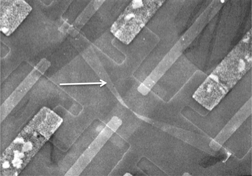
Figure 1.11. In this figure, a similar mesa has been created by the same processes as those of figure 1.10. The arrow indicates a connection line on the mesa that has been made by electron-beam lithography and liftoff. The width of the mesa is 40 µm. (Reproduced with permission of D Pivin.)
Download figure:
Standard image High-resolution image
In addition to the common etching approaches mentioned above, there are many other approaches to this process. Some often seen approaches include ion-beam etching, reactive-ion-beam etching, and chemically assisted ion-beam etching, in which the latter ones use a form of reactive gas or chemical vapor to assist the ion beam in its work.
Problems
1. Consider a normal MOS structure on Si at room temperature. Using the classical approach described in the chapter to determine the effective width of the inversion layer, compute the width for densities of 5 × 10¹¹, 1 × 10¹², 3 × 10¹², 5 × 10¹², 1 × 10¹³, all in units of cm−2. Assuming an acceptor density of 5 × 10¹⁷, compute the effective electric field in the oxide. Plot both the effective thickness and the effective electric field as a function of the inversion density on a single plot, using a logarithmic axis for the density.
2. Go to nanoHUB.org and launch the 'bound states calculation lab'. Using the data for the Si MOS structure above, and using the heavy mass for the Si inversion layer, enter the effective electric fields computed in the previous problem. Using the triangular geometry to approximate the inversion layer, determine the effective thickness of each of the first four subbands as a function of the inversion density corresponding to the effective electric field entered in the program.
3. Consider a uniformly doped GaAlAs layer, with a composition of x = 0.25, grown on top of a GaAs layer. If the Fermi energy is pinned 0.85 eV below the conduction band edge at the surface, what is the minimum thickness of the GaAlAs layer for it to be completely depleted of electrons? Assume the donor ionization energy is 50 meV and the donor density is 1018 cm−3.
4. Consider two exposure pixels of an electron-beam lithography system. Each exposure pixel is characterized by a Gaussian beam with a full-width half-maximum of 50 nm. If we assume that each Gaussian has a peak amplitude of unity, compute the exposure (amplitude of the signal) at the mid-point between the centroids of the Gaussians as they are moved from 20 nm center-to-center to 200 nm center-to-center.
5. Consider a 2DEG at the interface of a GaAlAs/GaAs heterostructure at 1.2 K. Assume that the electron density is 4 × 1011 cm−2 and the mobility is 500 000 cm2 Vs−1. (a) Determine the momentum relaxation time from the mobility, and then determine the diffusion coefficient using the Einstein relation (you may need to make some corrections for the Fermi–Dirac distribution function). (b) Estimate the diffusion coefficient from the Fermi energy and Fermi velocity. Is there a difference in the two values? Why?
6. Using the structure and data from problem 5, estimate the elastic mean free path for the electrons. If we assume that the device has a transport length of 1 cm, we can use this for the inelastic mean free path. What is the value of the phase-breaking time in this case?
References
- [1]Ferry D K, Goodnick S M and Bird J P 2009 Transport in Nanostructures 2nd edn (Cambridge: Cambridge University Press)
- [2]Zhou X, Dayeh S A, Aplin D, Wang D and Yu E T 2006 Appl. Phys. Lett. 89 053113
- [3]Ferry D K, Gilbert M J and Akis R 2008 IEEE Trans. Electron Dev. 55 2820
- [4]Shah J 1996 Ultrafast Spectroscopy of Semiconductors and Semiconductor Nanostructures (Berlin: Springer) See, e.g.,
- [5]Kilby J S 1959 Miniature semiconductor integrated circuit US Patent 3,115,581
- [6]Noyce R N 1959 Semiconductor device and lead structure US Patent 2,981,877
- [7]Moore G E 1965 Electronics 38 114–117
- [8]Dennard R H, Gaensslen F H, Rideout V L, Bassous E and LeBlanc A R 1974 IEEE J. Sol.-State Circuits 9 256
- [9]Keyes R 1977 Science 195 1230
- [10]Kelly M J 1995 Low-Dimensional Semiconductors: Materials, Physics, Technology, Devices (Oxford: Clarendon) See, e.g.,
- [11]Khoury M and Ferry D K 1996 J. Vac. Sci. Technol. B 14 75
- [12]Tao N J, Derose J A and Lindsay S M 1992 J. Phys. Chem. 97 910
- [13]Bimberg D, Grundmann M and Ledentsov N N 1999 Quantum Dot Heterostructures (Chichester: Wiley) See, e.g.,
- [14]Crommie M F, Lutz C P and Eigler D M 1993 Science 262 218
- [15]Mott N F 1970 Phil. Mag. 22 7
- [16]Thouless D J 1974 Phys. Rep. 13C 93Edwards J T and Thouless D J 1972 J. Phys. C: Solid State Phys. 5 807Licciardello D C and Thouless D J 1975 J. Phys. C: Solid State Phys. 8 4157Thouless D J 1977 Phys. Rev. Lett. 39 1167
- [17]Abrahams E, Anderson P W, Licciardello D C and Ramakrishnan T V 1979 Phys. Rev. Lett. 42 673
- [18]D'Iorio M, Pudalov V M and Semenchinsky S G 1992 Phys. Rev. B 46 15992
- [19]Kravchenko S V, Mason W, Furneaux J E and Pudalov V M 1995 Phys. Rev. Lett. 75 910
- [20]Pudalov V M, Brunthaler G, Prinz A and Bauer G 1998 Physica E 3 79
- [21]Lin J J and Giordano N 1987 Phys. Rev. B 35 1071
- [22]Mohanty P, Jariwala E M Q and Webb R A 1997 Phys. Rev. Lett. 78 3366
- [23]Lilienfeld J E 1926 Method and apparatus for controlling currents US Patent 1,475,175
- [24]Atalla M M, Tannenbaum E and Scheibner E J 1959 Bell Syst. Tech. J. 38 749
- [25]von Klitzing K, Dorda G and Pepper M 1980 Phys. Rev. Lett. 45 494
- [26]Skocpol W J, Mankiewich P M, Howard R E, Jackel L D, Tennant D M and Stone A D 1987 Phys. Rev. Lett. 58 2347
- [27]Koch J F 1976 Surf. Sci. 58 104
- [28]Wilmsen C W 1976 Thin Solid Films 39 105
- [29]Baglee D A, Ferry D K and Wilmsen C W 1980 J. Vac. Sci. Technol. 17 1032
- [30]Neamen D A 2012 Semiconductor Physics and Devices 4th edn (New York: McGraw-Hill)
- [31]Tsividis Y 1999 Operation and Modeling of the MOS Transistor 2nd edn (New York: McGraw-Hill)
- [32]Ando T, Fowler A and Stern F 1982 Rev. Mod. Phys. 54 437
- [33]SCHRED 2.0, https://nanohub.org/resources/schred
- [34]Ando T 1977 J. Phys. Soc. Japan 43 1616
- [35]Goodnick S M, Ferry D K, Wilmsen C W, Liliental Z, Fathy D and Krivanek O L 1985 Phys. Rev. B 32 8171
- [36]Masaki K, Taniguchi K and Hamaguchi C 1992 Semicond. Sci. Technol. 7 B573
- [37]Suzuki Y, Seki M and Okamoto H 1984 16th Congr. on Solid State Devices and Materials (Tokyo) 607
- [38]Heiblum M, Nathan M I and Eizenberg M 1985 Appl. Phys. Lett. 47 503
- [39]Schubert E F and Ploog K 1965 Japan. J. Appl. Phys. 24 L608
- [40]Dingle R, Störmer H L, Gossard A C and Wiegmann W 1978 Appl. Phys. Lett. 33 665
- [41]Pfeiffer L, West K W, Störmer H L and Baldwin K W 1989 Appl. Phys. Lett. 55 1888
- [42]Lin B J F, Tsui D C, Paalanen M A and Gossard A C 1984 Appl. Phys. Lett. 45 695
- [43]Mooney P M 1990 J. Appl. Phys. 67 R1
- [44]Bound state calculation lab https://nanohub.org/resources/4875?rev=29
- [45]Ambacher O et al 1999 J. Appl. Phys. 85 3222
- [46]Howard R E, Liao P F, Skocpol W J, Jackel L D and Craighead H G 1983 Science 221 117
- [47]Rensch D B, Seliger R L, Csanky G, Olney R D and Stover H L 1979 J. Vac. Sci. Technol. 16 1897
- [48]Khoury M and Ferry D K 1996 J. Vac. Sci. Technol. B 14 75
- [49]Bernstein G, Ferry D K and Liu W 1989 Process of obtaining improved contrast in electron beam lithography US Patent 4,937,174
- [50]Bernstein G H and Hill D A 1992 Superlattices Microstruct. 11 237
- [51]Bernstein G H, Liu W P, Khawaja Y N, Kozicki M N, Ferry D K and Blum L 1988 J. Vac. Sci. Technol. B 6 2296
- [52]Tennant D M, Jackel L D, Howard R E, Hu E L, Grabbe P, Capik R J and Schneider B S 1981 J. Vac. Sci. Technol. 19 1304
- [53]Crook R, Graham A C, Smith C G, Farrar I, Beere H E and Ritchie D A 2003 Nature 424 751
- [54]Song H J, Rack M J, Abugharbieh K, Lee S Y, Khan V, Ferry D K and Allee D R 1994 J. Vac. Sci. Technol. B 12 3720
- [55]Fuhrer A, Dorn A, Lüscher S, Heinzel T, Ensslin K, Wegscheider W and Bichler M 2002 Superlattices Microstruct. 31 19
- [56]Prasad C. private communication
- [57]Pivin D 1998 PhD Dissertation (Tempe, AZ: Arizona State University)