
Abstract
This paper reviews recent progress in an energy-autonomous biosensing platform using a supply-sensing CMOS integrated sensor and a biofuel cell for next-generation healthcare Internet of Things (IoT). By introducing an energy-efficient supply-sensing architecture with CMOS electronics, energy-autonomous operation become feasible. In the supply-sensing architecture, energy harvesting and sensing are combined, and thus the energy efficiency can be dramatically improved. This paper also introduces some examples of energy-autonomous sensing platforms, i.e., fructose-, lactate-, and glucose-monitoring applications.
Export citation and abstract BibTeX RIS
1. Introduction
For improving quality of life (QoL) at today's aging society, healthcare and medical electronics are intensively developed. However, the performance of healthcare and medical electronics such as IoTs are limited by energy budget. Now, we are facing "energy-limited" era, where every performance is limited by energy. While, energy efficiency of CMOS electronics is being improved even in these days. By demand for smartphone industry, CMOS transistors are being improved from the view point of energy efficiency.
In these energy-limited era, ensuring stable energy is one of the most important current challenges in wearable and implantable healthcare devices as shown in Fig. 1. To address this issue, many developments with respect to batteries,1) wireless power delivery,2) and energy harvesting3) have been reported. Although technical improvements in these areas have been rapid, none of them fully satisfy the requirements. Batteries are unsuitable for use near the human body for safety reason. Even though encased batteries are commonly used in pacemakers, some people do not want to accept in-body battery from psychological reason. Besides, generally speaking encased batteries are costly. Wireless power delivery requires a large power-receiving antenna, and energy harvesting is unstable for healthcare application. Additionally, the latter two approaches require power management units such as power receivers, AC–DC converters, and DC–DC converters which consume area and increase cost.
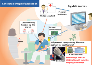
Fig. 1. Conceptual diagram of the application of the proposed supply-sensing biosensor platform.
Download figure:
Standard image High-resolution imageAs an alternative energy source, bio fuel cells have been intensely developed for applications such as disposable transdermal iontophoresis patches4–6) and brain–machine interfaces.4) Bio fuel cells are safe, stable and do not require an antenna or AC–DC converter. Additionally, the amount of energy obtained from the human body can be used as bio sensing data, and thus the sensor electrodes and front-ends become unnecessary. Of the bio fuel cells, the organic bio fuel cell4–6) is especially promising because it is cheap and environmentally friendly, which enables disposable healthcare. However, the output supply voltage from a bio fuel cell is usually lower than 0.4 V, and conventional circuits cannot operate using bio fuel cells without power management circuits. Thus, a new circuit technique must be developed for converter-less operation.
2. Supply-sensing architecture
In order to address the demand for low-voltage operation, we have proposed new circuit architecture. Figure 2 shows the circuit diagram of the proposed supply-sensing biosensor platform, which consists of three parts: the bio fuel cells, supply-controlled oscillator (SCO), and a wireless transmitter. The different points from the conventional topologies are followings:
- Elimination of the power management circuits, clock sources, and ADCs.
- Introduction of SCO.
By eliminating the area-hungry power management circuits, sensing front-end circuit, power-hungry clock source such as PLLs, and power-hungry analog-to-digital converters (ADC), the occupied area and required power can be dramatically reduced. By introducing SCO, the supply voltage can be transduced to frequency.

Fig. 2. Proposed supply-sensing biosensor platform compared to conventional platforms.
Download figure:
Standard image High-resolution imageIn the next session, examples of application of energy-autonomous sensing are introduced.
3. Application of energy-autonomous sensing
This section introduces some applications for energy-autonomous sensing: fructose sensing, lactate sensing, and glucose sensing.
3.1. Fructose sensing (first prototype)
Firstly, we have tried to develop fructose sensing system because excellent enzyme for fructose fuel cell has been established. As a first prototype, we have developed the following device.
3.1.1. Circuit architecture of first prototype.
Figure 3 shows the circuit diagram of the first prototype. It consists of three parts: the fructose fuel cell, SCRO, and an inductive-coupling transmitter. By introducing digital-based SCRO, the required minimum supply voltage can be reduced. Besides, by introducing the current-driven inductive-coupling link, low-voltage operation can be possible.
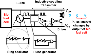
Fig. 3. Circuit diagram of the proposed supply-sensing biosensor platform.
Download figure:
Standard image High-resolution imageTo minimize the supply voltage, a fully digital, current-driven architecture was employed. Implementing the proposed architecture using zero-Vth transistors enables a low-supply voltage of less than 0.4 V to be used. Zero-Vth transistors are commonly available on both the state-of-the-art and legacy CMOS technologies. Thus, our technique can be feasible even in other technologies. Because the supply-sensing scheme is unsuitable for pulse amplitude modulation owing to its nature, time-domain modulation must be employed. To minimize power consumption, pulse-interval modulation (PIM) was employed in this work as shown in Fig. 4.

Fig. 4. Operation principles of the proposed supply-sensing biosensor platform. Pulse interval modulation (PIM) is adopted.
Download figure:
Standard image High-resolution image3.1.2. Fructose fuel cell.
In the proposed supply-sensing biosensor platform, the bio fuel cell has two functions: energy harvesting and front-end sensing. Typical bio fuel cells can generate a voltage of less than 0.4 V.4–6) Thus, to realize self-powered operation without large and expensive power management circuits such as up-converters, the circuits must operate with a supply voltage of less than 0.4 V.
In order for bio fuel cells to function as both a power source and sensing front-end, the anode and cathode must be designed carefully. Unlike typical biosensors based on one transducer, the proposed supply-sensing biosensor uses two transducers (anode and cathode). Thus, if the output power depends on unintended transducers, the proposed device cannot function as a sensor even if it functions well as power source.
For aiming practical application, glucose or lactate fuel cells are beneficial because it can be used for glucose or lactate monitoring. However, they are under development and not available for us. As a preliminary study, we have chosen fructose fuel cell. Though fructose is not available on the human body and it has no healthcare application, it is meaningful as a preliminary study. Since the energy generation mechanism of fructose fuel cell is similar to that of glucose and lactate fuel cells, this study will contribute the successive research and development.
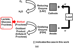
In the case of our prototype fructose sensor, we use the following reactions: in the anode, the capability to product current depends on fructose concentration. In the cathode, the capability to product current depends on oxygen concentration. To sense fructose, the total output current must depend on not oxygen but fructose, which we achieve by adjusting the sizes of the anode and cathode.
The biofuel cell in this work is an enzymatic fuel cell. Figure 5(a) shows the conceptual image of the mechanism of power generation from the bio fuel cells. Two kinds of enzymes, d-fructose dehydrogenase (FDH; EC 1.1.99.11, 169.9 U mg−1, ca. 140 kDa, from Gluconobactor, purchased from Toyobo Enzyme) and laccase (LAC; EC 1.10.3.2, 108 U mg−1, ca. 60 kDa, from Trametes sp, purchased from Daiwa Kasei) are immobilized to anode and cathode, respectively. They can directly catalyze the oxidation of d-fructose and the reduction of dioxygen, respectively. We used the FDH as received without further purification. While, the LAC was purified by anion exchange chromatography with a DEAE-Toyoperal column.
Download figure:
Standard image High-resolution image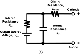
Download figure:
Standard image High-resolution image
Fig. 5. Conceptual image of the mechanism of power generation from the bio fuel cells (a), its detailed equivalent electrical circuit model (b), and its simplified equivalent electrical circuit model (c).
Download figure:
Standard image High-resolution imageIt is really important for the bio fuel cells to be safe in human use from the viewpoint of practical application. These enzymes are safe and suitable for human use. By exploiting these enzymes, following chemical reactions are occurred.


As a result of the above chemical reaction, electrons are transferred from the anode to cathode, and energy can be available at the load devices.
3.1.3. SCRO and inductive-coupling transmitter.
To achieve PIM, the supply voltage must be modulated using pulse intervals. To enable low-voltage operation, we implemented an SCRO. The SCRO consists of a normal ring oscillator with inverter cells. As the inverter cell, the standard cell using one NMOS and one PMOS from the foundry were utilized.
For the wireless transmitter, we implemented a current-driven, inductive-coupling transmitter. Considering the limited power budget, proximity communication without any security protection was adopted. Commonly-used electrical proximity communication can be categorized into two approaches: the capacitive-coupling links and inductive-coupling links. Figure 6 shows their conceptual operating principles. The voltage obtained at the receiver side of a capacitive-coupling link is determined by the ratio of the coupled capacitance to the total capacitance. Thus, a voltage that is higher than the transmit voltage cannot be received.

Fig. 6. Operating principle of two kinds of the proximity communication techniques.
Download figure:
Standard image High-resolution imageIn contrast, the voltage received in the inductive-coupling link is determined by a product of the slew rate of the transmit current and mutual inductance. A high received voltage can be obtained, even with a low supply-voltage transmitter. Bio fuel cells can generate larger currents at lower tages because of their characteristics;4) thus, a current-driven inductive-coupling link is preferable.
There is a trade-off between power supply voltage and the technology node. The lowest supply voltage was 0.7 V35) for the clock-based synchronous inductive-coupling link, and none of the conventional proximity communications could satisfy the requirement for operation with bio fuel cells. This work achieved the lowest supply voltage using the most cost-competitive technology node. The inductive-coupling transmitter was designed as described in the literature.21)
3.1.4. Prototyping and results.
To verify the effectiveness of the proposed approach, a test chip was fabricated using 0.25-µm CMOS technology with a nominal supply voltage of 2.5 V. Figure 7 shows a microphotograph of the test chip. The measurement setup is shown in Fig. 8.
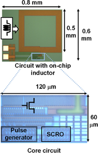
Fig. 7. Chip microphotograph of the proposed supply-sensing biosensor platform in 0.25 µm CMOS.
Download figure:
Standard image High-resolution image
Fig. 8. Measurement setup. A magnetic probe was utilized to confirm the generation of magnetic flux from the test chip.
Download figure:
Standard image High-resolution imageFigures 9 and 10 show the measured current, power consumption, and output frequency as a function of supply voltage. Operation with 0.23 V power supply was verified. A supply of 0.23 V is sufficiently low for self-powered operation using a bio fuel cell and is the lowest supply voltage ever reported for proximity communications. Because the drain current of a zero-Vth transistor is proportional to the square of gate–source voltage VGS from 0 to 0.4 V and is proportional to VGS from 0.4 V, the current consumption characteristics change at 0.4 V.
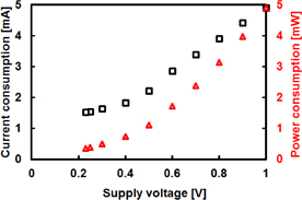
Fig. 9. Measured current and power consumption as a function of supply voltage. Operation at 0.23 V was verified.
Download figure:
Standard image High-resolution image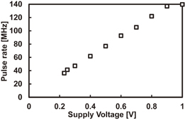
Fig. 10. Measured pulse-rate as a function of supply voltage.
Download figure:
Standard image High-resolution image3.1.5. Demonstration of energy-autonomous fructose sensing.
To verify the effectiveness of the proposed platform, self-powered operation using an organic bio fuel cell1,2) was demonstrated. The bio fuel cell has a cloth-like feature. The enzymes for energy generation were immobilized on the bio fuel cell. Figure 11 shows a summary of the measured performance of the bio fuel cell. Figures 11(a) and 11(b) are performance of the anode and cathode, respectively. Figure 11(c) is the overall performance including both anode and cathode. By changing the load resistance, each measurement point was obtained. Figure 11(d) shows the measurement setup. The measurement was performed using a three-electrode system (BSA 730C electrochemical analyzer).
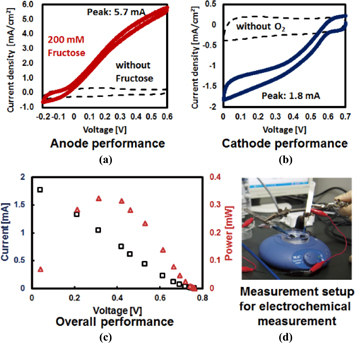
Fig. 11. Measured performance of the bio fuel cell and its measurement setup used to measure the results. (a) Anode performance. (b) Cathode performance. (c) Overall performance. (d) Measurement setup.
Download figure:
Standard image High-resolution imageFigure 11 shows successful self-powered operation using the bio fuel cell. By dipping the bio fuel cell into a fructose solution, the circuit transmitted a magnetic field, and its waveform appeared on the oscilloscope. This work is the first demonstration of a self-powered CMOS-based proximity transmission using bio fuel cells and SCRO.
Figure 12 shows a summary of the self-powered operation. Figure 13(a) shows the output voltage and current of the bio fuel cell as a function of fructose concentration. The voltage and current increased as the fructose concentration increased. Figure 13(b) shows the measured pulse rate of the output magnetic field from the proposed biosensor platform. The pulse rate increased as the fructose concentration increased. From these measured results, we have successfully confirmed the feasibility of the proposed self-powered supply-sensing biosensor platform.

Fig. 12. Demonstration of self-powered operation using an organic bio fuel cell. When the bio fuel cell is dipped into a fructose solution, the proposed biosensor transmits a magnetic pulse.
Download figure:
Standard image High-resolution image
Download figure:
Standard image High-resolution image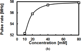
Fig. 13. Measured output voltage from bio fuel cell (a) and measured pulse rate (b) as a function of fructose concentration.
Download figure:
Standard image High-resolution image3.2. Lactate sensing (second prototype)
For targeting healthcare application, we have developed lactate sensing. Lactate monitoring is beneficial for athletic training. Figure 14 shows the conceptual image of the proposed lactate sensing. This sub section is related to the literature.
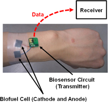
Fig. 14. Conceptual image of the proposed lactate sensing.
Download figure:
Standard image High-resolution image3.2.1. Circuit architecture of second prototype.
Figure 15 shows a block diagram of the proposed bio-sensing system, which consists of four building blocks: biofuel cells, a digital-based gate leakage timer, a supply-insensitive temperature sensor, and an inductive-coupling link. On the transmitter side, all circuitry is powered by a biofuel cell without regulation and voltage boosting. Consequently, the circuitry needs to be able to tolerate low-power and low-voltage operation. The digital-based gate leakage timer is used for supply sensing, and converts the supply voltage VDD to the pulse period, which is depends on the bio-concentration. Because the supply-sensing scheme is intrinsically unsuitable for pulse amplitude modulation, pulse-interval modulation (PIM) is employed. The supply-insensitive time-domain temperature sensor, which is used to calibrate the supplied voltage from the biofuel cells, generates a temperature-dependent time-domain output. The inductive-coupling transmitter transmits the signal to the receiver side.

Fig. 15. Block diagram of the proposed lactate sensing.
Download figure:
Standard image High-resolution image3.2.2. Simultaneous temperature sensing.
For proper operation, the relationship between the timer and temperature sensor needs to be understood. Figure 16 shows the required output properties of the timer and temperature sensor. Based on these requirements, it is necessary that these devices oppositely sensitive to the supply voltage and temperature. The principle of operation the system when the bio-concentration and temperature change overtime is shown in Fig. 17. The timer converts the supply voltage into a period with inherently temperature-insensitive properties. Subsequently, the time-domain temperature sensor outputs the temperature information with supply-voltage-insensitive properties. The combination of the temperature-insensitive timer and supply-insensitive temperature sensor enables reliable healthcare monitoring using biofuel cells.

Fig. 16. Required output properties of the timer and temperature sensor.
Download figure:
Standard image High-resolution image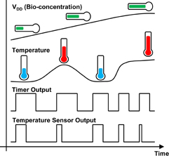
Fig. 17. Operating principle of the proposed bio-sensing system.
Download figure:
Standard image High-resolution image3.2.3. Prototyping and results.
The test transmitter chip of the proposed system is shown in Fig. 18(a), and was fabricated using 65 nm CMOS technology with an active area of 0.0032 mm2. The advanced CMOS technology was used because it enabled the low-voltage and low-power operation of the transmitter in a small footprint. In practical applications, the transmitter sensor board can be stacked on top of the biofuel cell, and the occupied area will therefore be constrained to that of the biofuel cell.

Fig. 18. Microphotographs of the prototype sensor boards and CMOS test chips: (a) transmitter in 65 nm CMOS, and (b) receiver in 0.25 µm CMOS (c) measurement setup.
Download figure:
Standard image High-resolution imageThe asynchronous receiver circuit was fabricated with 0.25 µm CMOS technology and had an active area of 0.035 mm2, as shown in Fig. 18(b). This legacy CMOS technology was selected for cost reasons. The receiver sensor board was focused on verification of the inductive-coupling communications method, and did not include circuit techniques, such as calibration or statistical processing, in this work.
To validate the design of the timer and temperature sensor, the outputs of both the supply and temperature sensor must follow the properties shown in Fig. 3. The characteristics of the test chips of the timer and temperature sensor were measured inside a constant temperature oven. The experimental setup is shown in Fig. 12. The measured samples of the timer and temperature sensor operated correctly.
Figure 19 shows the measured output frequency across five samples and temperature sensitivity of the timer. The frequency increased with the supply voltage. The measurements revealed that the average frequency was 1.83 kHz at a supply voltage of 200 mV with a standard deviation of 130 Hz (or 6.83%). An almost linear relationship between the frequency and supply voltage was confirmed at room temperature. Keysight 34465A was used to characterize the resolution of the timer (supply-sensing sensor). The resolution was 0.001 mV with the average sensitivity of 5410 ppm/mV over the supply voltage range of 200–400 mV, as shown in Fig. 19(a). On the other hand, from the result of Chip 1, the temperature sensitivities were 3200 and 1330 ppm/°C at supply voltages of 200 and 400 mV, respectively, as shown in Fig. 19(b). The frequency variation resulted in a voltage inaccuracy of 31 and 24 mV at supply voltages of 200 and 400 mV, respectively. The temperature impact on the frequency variation is mainly due to the temperature-related threshold voltages of the two inverters in the Schmitt trigger of the timer. Therefore, the frequency variation of the timer against temperature was reduced at the higher supply voltage with the nearly superthreshold region operated digital circuitry in the timer. Figure 19(c) shows the measured linearity of the timer. The voltage inaccuracy of the timer was within −36/+43 mV. Figure 20 shows the measured power consumption of the timer as a function of the supply voltage. The power consumption of the timer reached a minimum of 7.3 nW at a supply voltage of 200 mV with a standard deviation of 3.1 nW (or 31%). Figure 21 shows the measured setup and communication results. Figure 22 shows the measured power consumption.

Download figure:
Standard image High-resolution image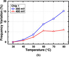
Download figure:
Standard image High-resolution image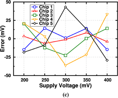
Fig. 19. (a) Measured frequency of the timer as a function of the supply voltage for the five samples at room temperature, (b) measured frequency variation as a function of temperature of Chip 1, and (c) measured linearity of the timer.
Download figure:
Standard image High-resolution image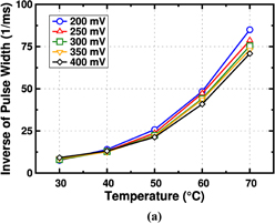
Download figure:
Standard image High-resolution image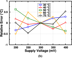
Download figure:
Standard image High-resolution image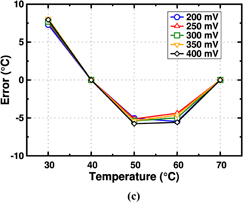
Fig. 20. (a) Inverse of measured output of the temperature sensor as a function of temperature, (b) measured relative error as a function of the supply voltage, and (c) measured temperature error after two-point calibration.
Download figure:
Standard image High-resolution image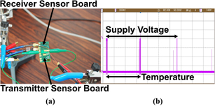
Fig. 21. Demonstration of inductive-coupling communication: (a) measurement setup and (b) measured result.
Download figure:
Standard image High-resolution image
Fig. 22. Measured power consumption of the transmitter as a function of the supply voltage.
Download figure:
Standard image High-resolution image3.3. Glucose sensing (third prototype)
At present, diabetes has become one of the most serious life-style diseases, making it necessary for the development of a low-invasive continuous glucose monitoring system (CGMS). In order to address this issue, an RFID-based smart contact lens, which uses the smart glass as the reader and utilizes RF wireless power transfer and backscatter communication, has been developed.9) However, this requires a dedicated glass, which degrades the patients' comfort and privacy. Besides, the conventional one cannot be used during sleep and cannot detect neither nighttime diabetes nor nocturnal hypoglycemia.
3.3.1. Circuit architecture of third prototype.
In this work, we firstly demonstrate the potential of using a combination of low-power CMOS OOK transmitter and glucose fuel cell for the development of glass-free CGMS contact lens. The recent progress in the field of biofuel cells has enabled the fabrication of glucose fuel cells on silicon wafer.37) It is capable of achieving an output of 2.3 µW/cm2 and an open-circuit voltage of 0.55 V, which is maintained for at least 48 h. In the fuel cell, glucose oxidation and oxygen reduction occurs in the anode and cathode, respectively. Under an oxygen-rich environment with oxygen-permeable contact lens, the output power depends on glucose concentration. Therefore, a self-powered independent CGMS, which does not require any external signal nor power can be developed by combining it with a supply-modulated OOK transmitter. By using the fuel cells as both the power source and sensing transducer from tear's glucose concentration, the costly off-chip antenna for wireless power delivery and sensing electrodes can be avoided, which dramatically reduces production cost. Besides, since human blood glucose concentration is guaranteed to be higher than a certain level, the power supply from glucose is expected to be more stable than wireless power delivery or other energy harvesting sources.
A test chip was fabricated in 55-nm DDC CMOS technology featuring low-leakage and low-voltage operation. Except for the cross-couple NMOSs in the LC power oscillator and the switches in the switched-capacitor voltage multiplier, all the transistors are DDC transistors. For the purpose of reducing the fabrication cost, an on-chip antenna was implemented. The footprint of the CMOS prototype is 0.36 mm2 (0.6 mm × 0.6 mm), which is the same as that of the CMOS read-out chip in literature.9)
Figure 23 shows the conceptual image of the proposed CGMS. The entire system can be divided into two parts: Glucose fuel cell and CMOS chip. The size of the fuel cell is same as that of the CMOS chip. The miniaturization was achieved by introducing RIE.38) Since the output power depends only on the glucose concentration under an oxygen-rich environment, the fuel cell can be used as both the sensing transducer as well as the power source.39) For example, higher glucose concentration results in higher output power and higher transmission rate, and vice versa. This architecture eliminates the requirement of a sensor part, which requires a large area as in the prior art.9) The CMOS chip is capable of supply-modulated OOK wireless transmission. The chip consists of on-chip-inductor-based boost-converter, self-oscillating-voltage-doubler-based control circuit, and LC power oscillator. Two chips are integrated in the PCB board, and the total size is less than 1 mm3.
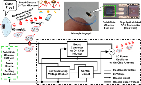
Fig. 23. Conceptual image of the proposed OOK transmitter for glass-free continuous glucose monitoring system (CGMS).
Download figure:
Standard image High-resolution imageFigure 24 shows the schematics of the proposed circuit of a boost converter and an RF LC-based power oscillator including its simulated result. To improve compatibility with volume-limited contact lens application, an off-chip-inductor-based boost converter40) cannot be adopted. However, the conventional switched-capacitor-based converter41) cannot satisfy our requirement from the viewpoint of leakage current. For reducing leakage current with a small volume, we implemented on-chip-inductor-based boost converter. In order to compensate low-efficiency of the boost converter due to low-performance of an on-chip inductor, the LC power oscillator is activated with much lower frequency than the boost converter as shown in the simulated waveform. Time resolution of several seconds is sufficient for CGMS application. Low-Vth NMOSs are implemented in the cross-couple part of LC power oscillator. The control signals are fed into by the control circuitry described as followings.
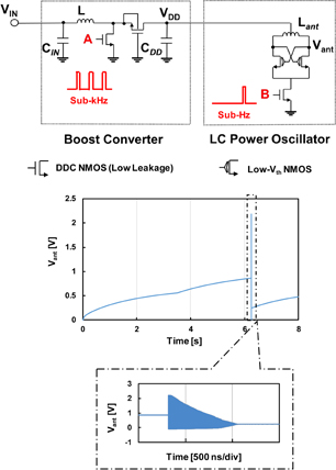
Fig. 24. Circuit diagram of the boost converter and LC power oscillator and simulated waveform.
Download figure:
Standard image High-resolution imageFigure 25 shows the schematic and simulated waveform of the control circuit. The control circuit consists of FF-based clock divider, pulse generators, switched-capacitor-based voltage multipliers. A self-oscillating voltage doubler42) provides the boost conversion and clock signal. Since insufficient slew rate in activation signal (A) increases dynamic loss in the boost converter, high slew rate operation must be achieved. Therefore, the supply voltage of the control circuit was provided by the voltage doubler. This is also helpful for reducing the required number of stages of large-leakage switched-capacitor-based voltage multiplier. The clock divider generates sub-Hz activation signal (B), of which division ratio is determined to guarantee the oscillation of LC power oscillator.
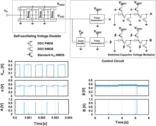
Fig. 25. Circuit diagram of the self-oscillating voltage doubler and control circuit and simulated waveform.
Download figure:
Standard image High-resolution image3.3.2. Glucose fuel cell.
Figure 26 shows the operating principle of the developed CMOS-compatible glucose fuel cell.7,47) Ideal glucose fuel cells obtain energy from the following chemical reactions:


However, glucose is not completely oxidized when its oxidation is mediated by Raney platinum7) but mainly oxidized to gluconic acid by the following chemical reactions:


As shown above, glucose oxidation and oxygen reduction are respectively caused at the anode and cathode. The theoretical maximum OCV is 1.30 V.45,48)
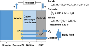
Fig. 26. Conceptual image and operating principle of the developed CMOS-compatible glucose fuel cell.
Download figure:
Standard image High-resolution imageThe fabrication process of wafer-scale glucose fuel cell is shown in Fig. 27. The development procedure is based on previous study.7) The fabrication procedure of the cells is outlined as follows:
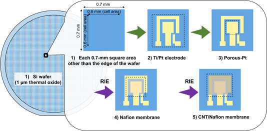
Fig. 27. Conceptual image of the fabrication procedure.
Download figure:
Standard image High-resolution image1) A 6-in. silicon wafer with 1-µm thermal oxide was prepared. We used a wafer with 625 µm thickness.
2) The electrode was prepared by depositing 2-nm-thick Ti and 100-nm-thick Pt layers. Ti was used as an adhesion layer.
3) A porous-Pt layer in the anode area was formed. The overall approach is etching Al from Al/Pt alloy. We deposited 100-nm-thick Al over Pt (deposited in 2) by evaporation and annealed to alloy the Al and Pt. After annealing, we etched the Al from Al/Pt alloy.7,49)
4) We formed a 0.83% Nafion solution via  dilution in isopropyl alcohol (IPA) from Nafion liquid dispersion (Nafion® perfluorinated resin solution 5 wt % in mixture of lower aliphatic alcohols and water, contains 45% water, Sigma-Aldrich) and spin-coated it at 1000 rpm. After spin coating of the Nafion solution, we heated the wafer at 60 °C for 30 min and 120 °C for 30 min. Patterned by photolithography using 1.5-µm OFPR-800 and etched resist and Nafion layer O2 ashing (reactive ion etching, RIE) until the resist disappeared. The Nafion layer existed after etching. The Nafion layer separates the anode and cathode by preventing the passage of anions through the membrane.
5) We formed CNT-based layer on the Nafion layer. The CNT [carbon nanotube, single-walled ≥95% carbon basis (≥99% as carbon nanotubes), 0.84 nm average diameter, Sigma-Aldrich] was mixed in 0.83% Nafion solution described in 4). The CNT-based solution was dropped on the wafer heated about 100 °C (±20 °C). Patterned by photolithography using 1.5-µm OFPR-800 and etched resist and Nafion layer O2 ashing (RIE) until the resist disappeared. The CNT-based layer existed after etching. The difference between the method reported in Ref. 29 and the above process is the introduction of RIE instead of wet etching in the present process for the fabrication of the separator and cathode in step 4) and 5). The fabricated cells are in 0.36 mm2 (0.6 mm × 0.6 mm) and the wafer was cut into 0.7-mm square including 0.6-mm device size and 0.1-mm margin. The microphotograph and measurement setup is shown in Fig. 28.
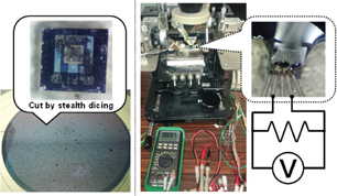
Fig. 28. Photograph of the developed prototype and its measurement setup.
Download figure:
Standard image High-resolution imageThe dependence of the measured output voltage and power on current is shown in Fig. 29. Figure 30 shows the dependence of the highest OCV in the measured samples. The measurement was performed with PBS-based 30-mM glucose concentration, which simulates the blood sugar level of diabetic patients in serious situation. Each point of the graph was measured by various load resistances. An OCV of 228 mV was verified. The power was 0.53 nW at peak with a load resistance of 2 MΩ, which corresponds to 1.32 µW/cm2 considering an anode area of 0.04 mm2. Considering the internal resistance of the tester (10 MΩ), the peak power was 5.2 nW.
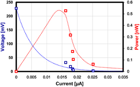
Fig. 29. Output voltage and power dependence on current of the cell with 228 mV OCV.
Download figure:
Standard image High-resolution image
Fig. 30. Output voltage as a function of glucose concentration.
Download figure:
Standard image High-resolution imageFigure 31 shows the correlation between the output voltage and glucose concentration. The output voltage get higher as glucose concentration increase. The PBS in the glucose solution resulted in an offset voltage when the glucose concentration was 0 mM. The sample cell used in this measurement was different from that shown previously.
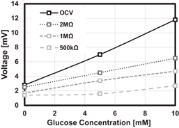
Fig. 31. Performance variation of the developed glucose fuel cells.
Download figure:
Standard image High-resolution imageFigure 32 shows the performance variation of the developed glucose fuel cells. We measured 132 samples to evaluate the performance variation. Six samples achieved over 100 mV of OCV.
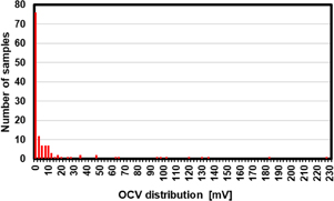
Fig. 32. Measurement setup and measured result of the supply current and period of wireless transmission dependence on supply voltage.
Download figure:
Standard image High-resolution image3.3.3. Prototyping and results.
Figure 33 illustrates testchip microphotograph, the measurement setup, and measured waveform of the supply current, and measured period of wireless transmission dependence on input supply voltage of the developed CMOS prototype. For simulating real-life environment with glucose fuel cell, only two signal are fed into the chip using a manual prober (Apollowave α100) and SMU (Keysight B2912A). The period of spike due to oscillation of LC power oscillator was increased by increment of input supply voltage from 320 to 400 mV. Periodical boost conversion whose period monotonically depends on the supply voltage was verified. This result implies the capability for supply-modulated OOK transmission.

Fig. 33. Measured supply current dependence on supply voltage.
Download figure:
Standard image High-resolution imageFigure 34 depicts the measured spectrum obtained by the developed CMOS prototype and its measurement setup. A 5-cm wireless transmission with 4.87 GHz center frequency was confirmed by the magnetic probe (LANGER MFA01), the amplifier (Beehive 150A), and the spectrum analyzer (Anritsu MS2830A). A wireless transmission of −34 dBm power under 10-dB attenuation was verified. The communication distance can be extended by introducing an external antenna.

Fig. 34. Measured spectrum obtained from the prototype chip.
Download figure:
Standard image High-resolution imageFigure 35 shows the performance comparison among the state-of-the-art low-power CMOS glucose sensor [1], a boost converter [5], and a pulsed transmitter with two input terminals [6]. Our proposed sensor outperforms the others in terms of current consumption while maintaining a competitive size. A current consumption of 6.1 nA at 0.32 V can be obtained using the 0.6-mm square glucose fuel cell [2,3]. Thus, this work demonstrates the feasibility of glass-free CGMS contact lens.

Fig. 35. Performance comparison.
Download figure:
Standard image High-resolution image
3.4. Discussions
By using supply-sensing architecture, CMOS bioelectronics7–34,36,43–46,50–69) can be energy autonomous. Thus, this will be beneficial for future healthcare and medical applications.
3.5. Comparison to other architectures
The advantages of the proposed supply-sensing architecture have been discussed in the paper. However, there are some issues required to be addressed as the future works. First of all, the measurement accuracy has not been investigated. Compared to the existing electrochemical-based glucose sensing,69) glucose fuel cells especially solid-state glucose fuel cells have been less examined. This is one of the disadvantages of the proposed technique.
Secondly, the required response time of the sensor has not been investigated. The existing electrochemical-based glucose sensing has been deeply developed for reducing response time. In the conventional architecture, the supply voltage is established and bias tages for the sensor is stable. While, our architecture inherently requires the start-up time for waking up the circuits. This may also become disadvantage.
4. Conclusions
The review introduces fusion of energy-efficient CMOS electronics and bio-fuel cells for enabling energy-autonomous biosensing platform. By exploiting energy-efficient supply-sensing architecture with bio fuel cells, energy-autonomous applications can be emerged. The proposed supply-sensing architecture has considerable potential for driving future healthcare and medical electronics.
Acknowledgments
This research was financially supported by JST, PRESTO (No. JPMJPR15D5), by JST, A-STEP (No. AS272S001b), by a Grant-in-Aid for Scientific Research (S) (Nos. 20226009, 25220906, 26220801), Grants-in-Aid for Young Scientists (A) (No. 16H06088) from the Ministry of Education, Culture, Sports, Science and Technology of Japan, by the Strategic Information and Communications R&D Promotion Programme (Nos. 121806006, 152106004) of the Ministry of Internal Affairs and Communications, Japan, by TOYOTA RIKEN, by the Hibi Science Foundation, and by The Nitto Foundation.
Biographies

Kiichi Niitsu (1983–) received B.S. (summa-cum-laude), M.S., Ph.D. degrees from Keio University, Japan, in 2006, 2008, 2010, respectively. He was JSPS Fellow (DC1). From 2010, he was Assistant Professor in Gunma University, Japan. From 2012, he was Lecturer in Nagoya University. Since 2018, he has been Associate Professor in Nagoya University. Since 2015, he has been concurrently JST/PRESTO Researcher. His research interests are VLSI design (54 journals, 115 conferences papers). He received 2017 Commendation for Science and Technology by Minister of MEXT, IEICE SUEMATSU-Yasuharu Award, IEEE BioCAS2016 Best Paper Award, FUNAI Research Promotion Award, Ando Incentive Prize, YASUJIRO-NIWA Outstanding Paper Award, and INOSE Science Promotion Award.