

Abstract
Room-temperature two-color lasing was demonstrated by current injection into a GaAs/AlGaAs coupled multilayer cavity for terahertz emitting devices utilizing its difference-frequency generation (DFG) inside the structure. We prepared two epitaxial wafers with (001) and (113)B orientations and they were directly bonded to form the coupled multilayer cavity. The (001) side cavity contains two types of InGaAs multiple quantum wells to realize optical gain for two-color lasing while a single GaAs layer of the (113)B side cavity is a nonlinear medium for efficient DFG. Lasing behavior was clearly observed for two modes under pulsed current conditions at room temperature. We found that the intensity relation between two-color lasings was dependent on the pulse duration because of the different temporal profiles of emission intensity. Simultaneous two-color lasing in the device was also confirmed by measuring the sum-frequency generation signal using a beta barium borate crystal.
Export citation and abstract BibTeX RIS
1. Introduction
Various kinds of terahertz (THz) light sources have been studied for many possible applications including wireless communication, spectroscopy, and imaging.1,2) The generation of ultrashort THz pulses has been extensively developed for time-domain spectroscopic applications based on recent femtosecond-laser technologies.3–5) Several types of continuous-wave THz emitters have also been studied and developed using semiconductor technologies. For example, quantum cascade lasers (QCLs),6–8) resonant tunneling diodes (RTDs),9,10) and photomixers11,12) have been reported so far. Recently, intracavity difference-frequency generation (DFG) in dual-wavelength mid-infrared QCLs has been demonstrated as a THz source.13,14)
We have proposed a GaAs/AlAs coupled multilayer cavity structure for compact and room-temperature operable THz emitting devices.15) The structure is composed of two equivalent cavity layers and three distributed Bragg reflector (DBR) multilayers. Two cavity modes appear in the center of the high reflection band because of the coupling of two equivalent cavities, and the number of the intermediate DBR pairs determines the mode frequency difference within the THz region. Utilizing the two cavity modes, we can generate a strong frequency-mixed signal owing to the enhanced electric field of each mode in both cavity layers. For this purpose, the structure should essentially be grown on a non-(001)-oriented GaAs substrate since the second-order nonlinear response is forbidden on a (001) substrate due to crystal symmetry.16) We have demonstrated a strong sum-frequency generation (SFG) signal from a GaAs/AlAs coupled multilayer cavity grown on a (113)B GaAs substrate by irradiating with 100 fs laser pulses whose frequency covers the two cavity modes.17–19) The DFG signal was also observed at room temperature by time-domain spectroscopy using a photoconductive antenna.20–22) We should take care of the spatial distribution of the nonlinear polarization to realize a large THz-DFG of two modes. It was theoretically and experimentally demonstrated that face-to-face bonding of two epitaxial wafers is an effective method for polarization control.23,24)
It is useful when two-color lasing is enabled in the coupled cavity structure by current injection because THz emission via DFG of two modes is possible without external light sources. Two mode emission characteristics in the near-infrared region have been studied by the optical pumping of self-assembled InAs quantum dots (QDs) that were introduced only in the upper cavity.25–27) We have also fabricated current-injection surface-emitting devices based on a wafer-bonded coupled cavity with QDs. Although we introduced nine layers of InAs QD in the active region, the lasing action has not been realized yet owing to insufficient optical gain.28) Carlin et al. demonstrated two-color lasing at room temperature by current injection into two-section vertical-cavity surface-emitting lasers where both cavities had gain regions consisting of InGaAs multiple quantum wells (MQWs).29,30) They also intentionally introduced an asymmetry in the two cavity lengths for stable two-color lasing. Recently, we have demonstrated two-color lasing from a strongly coupled two-cavity system that contains InGaAs MQWs only in the upper cavity.31,32) In that study, the entire structure of the coupled cavity was formed by epitaxial growth on a single substrate wafer, and two-color lasing of the device was observed by pulsed current injection at room temperature. A similar device was also fabricated and studied using the wafer-bonded GaAs/AlGaAs coupled cavity.33,34) The threshold behavior was observed in the current–light output (I–L) curve. However, two-color lasing was not realized at room temperature because of the wavelength mismatch between the cavity modes and the gain peaks of the MQWs.
In this study, we demonstrated room-temperature two-color lasing of the device using the coupled multilayer cavity with a finely tuned structure. The lasing properties were measured under pulsed conditions and their dependence on the pulse duration was also studied.35) In addition, we investigated the SFG signal by irradiating a beta barium borate (BBO) crystal to discuss the simultaneous two-color lasing of the device.
2. Device fabrication
Two epitaxial wafers, each of which had a single cavity structure, were prepared by molecular beam epitaxy (MBE) on 3-in.-diameter (001)- and (113)B-oriented GaAs substrates. The cavity length was 1.5 wavelengths (3λ/2) for both cavities, and GaAs/Al0.9Ga0.1As multilayers were grown as λ/4-DBRs. Three-period In0.15Ga0.85As/GaAs MQWs with two different well widths of 3.6 and 4.4 nm were inserted in the 3λ/2 cavity of the (001) epitaxial wafer while a single GaAs layer was used as the 3λ/2 cavity of the (113)B epitaxial wafer. Each MQW was located around the antinode of the electric field in the (001) side cavity for both modes. The thickness of each layer was carefully set to a specific value so that two-color lasing was enabled at room temperature. Note that slight lateral thickness variations were intentionally introduced for both the (001) and (113)B wafers to find a strongly coupled cavity system. Si and Be were used for n- and p-type dopants, respectively, and the concentration was approximately 2 × 1018 cm−3 for both the Si- and Be-doped DBRs, and a heavily Be-doped (∼3 × 1019 cm−3) GaAs layer was used as the p-type contact layer. Each GaAs/Al0.9Ga0.1As DBR multilayer had compositionally graded interfaces to reduce the electrical series resistance. Face-to-face bonding of the two epitaxial wafers was performed at room temperature by the conventional surface-activated bonding method.36,37) Note that the bonding interface should be closely set to the node of the electric field in GaAs for both modes to avoid optical loss at the bonding interface.28,33) Allowing this situation, we designed the structure in which a λ/4 GaAs layer nearest to the (113)B side cavity was replaced by a 3λ/4 GaAs layer. After the bonding, the wafer was cut into several chips with dimensions of 18 × 14 mm2. Then, the (001) GaAs substrate was thinned down to ∼20 µm by mechanical polishing and the remaining substrate was completely removed by selective wet etching using a citric acid-based etchant.38) Pairs of the top, middle, and bottom DBRs were 28, 12.5, and 34, respectively.
Figure 1 shows the schematic of the current-injection surface-emitting device. Using the coupled cavity structure prepared as described above, we carried out the following procedure. First, we defined circular mesas with diameters of 80–100 µm by a three-step wet etching process, which is composed of (1) etching of the p-type DBR using a phosphoric acid solution, (2) selective etching of the upper cavity using a citric acid solution, and (3) selective etching of the topmost AlGaAs layer of the n-type DBR using a more diluted phosphoric acid solution. The current confinement was accomplished by the lateral oxidation of a 44.1-nm-thick AlAs layer inserted just above the upper cavity with MQWs. The AlAs was selectively oxidized from the sidewall at 480 °C under a steam environment, which was supplied by bubbling nitrogen gas through deionized water maintained at 80 °C. Then, n-type electrodes were formed by depositing AuGe/Ni/Au (50/12.5/50 nm) onto the exposed n-type DBR surface, and the mesa structures were buried in polyimide film. Finally, p-type electrodes with the optical windows were formed by depositing Ti/Au (5/100 nm) onto the p-type DBR surface, followed by rapid thermal annealing at 430 °C in nitrogen atmosphere.

Fig. 1. Schematic of the surface-emitting device based on a GaAs/AlGaAs couple multilayer cavity that was fabricated by direct bonding of (001) and (113)B epitaxial wafers.
Download figure:
Standard image High-resolution image3. Lasing properties
The optical emission properties of the devices were studied at room temperature using a pulsed-current source with a repetition rate of 1 kHz. The pulse duration was varied from 0.5 to 5 µs. Figure 2 shows a picture of the fabricated device under pulsed operation at an injection current of 60 mA with a pulse duration of 0.5 µs. The I–L curve of each device was measured using an InGaAs p–i–n photodiode. The emission spectra under various operation conditions were also measured using a spectrometer with a thermoelectrically cooled Si charge-coupled device array. Two sharp peaks caused by the cavity modes were clearly observed in all the measured spectra. Note that the frequency difference between two modes was systematically varied across the wafer because both the (001) and (113)B epitaxial wafers were prepared to have a few percent thickness variation intentionally. Since two cavities with identical optical thicknesses were strongly coupled at the wafer position where the minimum frequency difference was observed, the devices located around this position were characterized in detail.
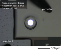
Fig. 2. Top view of the fabricated device under pulsed operation at 60 mA with a pulse duration of 0.5 µs.
Download figure:
Standard image High-resolution imageFigure 3 shows the I–L curves measured with various pulse durations. The threshold behaviors were clearly observed in all the I–L curves and the threshold current of ∼50 mA was almost the same for all the pulse durations. However, the decrease in the light output was significant for a long pulse duration of 5 µs because of heat generation in the device. Figure 4 plots the pulse duration dependence of the emission spectrum measured at the injection current of 90 mA, which was above the threshold current of the device. Two sharp peaks at 917.3 and 924.8 nm were clearly observed in all the spectra, indicating that room-temperature two-color lasing in the device was realized for each case. The optical frequency difference of two peaks was 2.65 THz. Since the measurements were performed under pulsed current conditions with small duty ratios of 0.05–0.5%, the device was repeatedly heated and cooled during the on- and off-states, respectively, which would be significant as the pulsed current was increased. Therefore, it can be considered that the threshold current is minimally dependent on the pulse duration because of the low injection current, while the decrease in the light output would become clearer for the higher injection current with the longer pulse duration. In addition, the spectra of Fig. 4 show the very slight spectral broadening for both peaks with increasing pulse duration. This is because spectral chirping occurred since the device was gradually heated up during the on-state. We also found that the spectral broadening due to the chirping became more significant and a slight peak shift was observed for the higher injection current. Note that the intensity relation between the two-color lasings was clearly dependent on the pulse duration. The emission intensity of the long-wavelength mode relative to the short-wavelength mode increased with increasing pulse duration. This might be due to the slight redshifts of the MQW gain peaks caused by the weak heat generation depending on the pulse duration. According to the spectral broadening, the temperature increase in the pulse duration can be roughly estimated as several degrees Celsius, which causes only a few nanometers redshifts of the bare MQW gain peaks. On the other hand, the magnitude of each modal gain is strongly dependent on the energy distribution of injected carriers under the laser oscillation. Therefore, when modal gains for two-color lasing correlate with each other, the intensity ratio between two modes will be strongly affected by such a small increase in the temperature. In fact, we already reported that the two-color lasing in the device was enabled by tuning the operating temperature at around 190 K and the intensity ratio was significantly varied in the narrow temperature range of 188–192 K.34) The cross-correlation between the modal gains might originate from the two dimensional electronic structure in the MQW system. The observed feature partly affects the THz generation in the device since the DFG is efficient when two-color lasing is enabled with identical intensities.
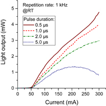
Fig. 3. Current-light output curves measured with various pulse durations at room temperature.
Download figure:
Standard image High-resolution image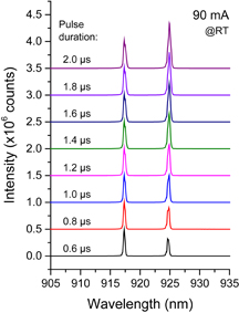
Fig. 4. Pulse duration dependence of the lasing spectrum at an injection current of 90 mA.
Download figure:
Standard image High-resolution imageSimultaneous two-color lasing in the device is crucial for efficient THz generation via the DFG process. The spectrum measurements such as those shown in Fig. 4 are insufficient to confirm the simultaneous two-color lasing since two spectral peaks could be observed even if each-color lasing occurred alternately by mode hopping. In this study, we carried out the SFG measurements using a BBO crystal. When the BBO crystal, which is well known as a nonlinear optical crystal, is irradiated with a two-color laser beam, an SFG signal can be observed between two second-harmonic generation (SHG) signals in the half-wavelength spectral region only for the simultaneous two-color lasing case. Thus, the SFG spectrum measurements were performed using the same spectroscopic system as used for the two-color lasing characterization shown in Fig. 4. Two-color emission from the device was focused onto a 1-mm-thick BBO crystal under a type I phase matching condition,39) and a blue band-pass filter was inserted to prevent the injection of fundamental two-color laser light into the optical fiber, which was used to collect the signal light before the spectral detection. In addition to the SFG spectrum, we also measured the fundamental two-color laser light spectrum by inserting a polarizer and removing the band-pass filter. Figure 5 shows the measured spectra when the device was operated at a current of 290 mA with a pulse duration of 0.5 µs and a repetition rate of 50 kHz. As shown in Fig. 5(a), an SFG signal was clearly observed between two SHG signals, indicating simultaneous two-color lasing in the device. However, the SFG signal intensity is about one-third of the expected value from the SHG signal intensities. The reduced SFG signal might be due to the different temporal profiles of two lasing peaks in the pulse duration as discussed below.
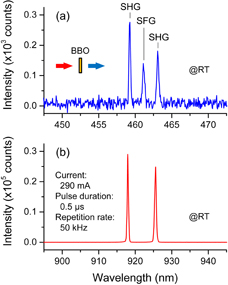
Fig. 5. (a) Spectrum of SHG and SFG signals measured by irradiating a BBO crystal with a two-color laser beam emitted from the device. (b) Two-color lasing spectrum used for the corresponding measurement.
Download figure:
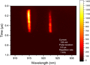
Standard image High-resolution imageThe temporal behavior of two-color lasing was studied for the device operated by the pulsed current injection. Figure 6 shows a time-resolved spectral map measured with a streak scope system. The injection current, pulse duration, and repetition rate were 105 mA, 0.5 µs, and 1 kHz, respectively. As can be seen in Fig. 6, the short-wavelength mode exhibited stronger emission in the initial stage, and the emission intensity of the long-wavelength mode increased with a slight delay. The observed behavior can be explained by the heat generation in the device by current injection. When the pulsed current was supplied to the device, the active layer was gradually heated up over time. In fact, both peaks showed slight redshifts owing to the refractive index change, which resulted from the temperature increase. In this case, the MQW gain peaks would exhibit larger redshifts than those of the cavity modes since the energy gap of the MQW is more strongly dependent on temperature than the refractive index. In the initial stage, the optical gain for the short-wavelength mode was larger than that for the long-wavelength mode because of the initial wavelength relationship between the MQW gain peaks and the cavity modes. Then, the MQW gain peaks would move to the longer-wavelength side because of the heat generation, which resulted in increased and decreased emission intensities for the long- and short-wavelength modes, respectively. Since we used the strongly coupled cavity system in the device, the electric field was distributed in both the upper (001) and lower (113)B cavity regions not only for the short-wavelength mode but also for the long-wavelength mode. Therefore, the redshifts should be observed for both modes even when an increase in the refractive index was induced only in the upper cavity by heat generation. If the generated heat was not sufficiently transferred from the upper cavity to the lower cavity, the effective optical thickness of the upper cavity became gradually larger than that of the lower cavity in the pulse duration. It might also be responsible for the different temporal intensity profiles of two lasing peaks observed in the time-resolved measurement. The temporal overlap of two-color lasing will be improved by the careful thermal management of the device.
Fig. 6. Time-resolved spectral map of the two-color lasing. The device was operated at 105 mA with a pulse duration of 0.5 µs and a repetition rate of 1 kHz.
Download figure:
Standard image High-resolution image
4. Conclusions
Room-temperature two-color lasing was demonstrated by current injection into a wafer-bonded GaAs/AlGaAs coupled multilayer cavity. The coupled cavity structure was fabricated by the direct bonding of (001) and (113)B epitaxial wafers prepared individually by MBE. The InGaAs MQWs with two different well widths were introduced only in the (001) side cavity as optical gain materials. We fabricated and characterized the current-injection surface-emitting devices based on the wafer-bonded coupled cavity. Lasing behavior was clearly observed for two modes under pulsed current conditions at room temperature. We also found that the intensity relation between two-color lasings was dependent on the pulse duration. Simultaneous two-color lasing in the device was confirmed by measuring the SFG signal using a BBO crystal. However, the SFG signal intensity was about one-third of the expected value. The measured time-resolved spectral map of two-color lasing revealed that the short-wavelength mode emission was dominant in the initial stage and the long-wavelength mode increased after a slight delay. The observed behavior can be understood in terms of heat generation caused by the current injection since it causes redshifts of the MQW gain peaks during operation. We should carefully consider the thermal management of the device since good temporal overlap of two-color lasing is reasonably efficient for THz generation via the DFG process.
Acknowledgment
This work was partly supported by JSPS KAKENHI Grant Number JP16H04351.