

Abstract
The mechanisms responsible for the effects of consecutive irradiation and negative bias temperature (NBT) stress in p-channel power vertical double-diffused MOS (VDMOS) transistors are presented in this paper. The investigation was performed in order to clarify the mechanisms responsible for the effects of specific kind of stress in devices previously subjected to the other kind of stress. In addition, it may help in assessing the behaviour of devices subjected to simultaneous irradiation and NBT stressing. It is shown that irradiation of previously NBT stressed devices leads to additional build-up of oxide trapped charge and interface traps, while NBT stress effects in previously irradiated devices depend on gate bias applied during irradiation and on the total dose received. In the cases of low-dose irradiation or irradiation without gate bias, the subsequent NBT stress leads to slight further device degradation. On the other hand, in the cases of devices previously irradiated to high doses or with gate bias applied during irradiation, NBT stress may have a positive role, as it actually anneals a part of radiation-induced degradation.
Export citation and abstract BibTeX RIS
1. Introduction
Development of semiconductor devices has affected technologies in various fields.1) Because of that there is a great interest for intensive research and improving the device performances.2) In many electronic devices, from metal–oxide–semiconductor field effect transistors (MOSFET) to bipolar integrated circuits (ICs), the parts based on dielectrics are key components. Silicon dioxide (oxide) SiO2 and oxide–semiconductor interface SiO2–Si are the most vulnerable parts of the MOS devices subjected to extreme, harsh environmental conditions or to the stress. Namely, irradiation, high electric field (HEF) stressing or bias temperature (BT) stressing lead to creation of oxide and interface defects which can cause degradation of electrical parameters of MOS devices. Hence, these defects have been in the focus of investigation more than 40 years.3–14)
Numerous methods used in the study of SiO2 and SiO2–Si interface nature and their characterization can be roughly divided into two categories: the methods implemented on the MOS capacitor structure and the methods implemented on the complex MOS electron devices. These methods are mostly based on electrical techniques and they generally yield the results related to the energy distribution of defects in the oxide and at the interface, thus allowing the prediction of the defect nature and modelling of their behavior. However, the method based on the electron-spin resonance (ESR),15) gives an image of the structure of these defects allowing their modelling.16) The silicon dangling bond defects detected on the SiO2–Si(111) interface, which are known as Pb centers, are the Si3≡Si• amphoteric defects with two energy levels in the silicon bandgap (0.3 and 0.85 eV above the valence band) serving as a correlation energy with broken bonds at SiO2–Si interface.17) Other investigations of the SiO2–Si(100) interface, which have been done by the method based on electron-paramagnetic resonance (EPR),18) revealed two paramagnetic centres Pb0 and Pb1. The Pb0 centre was found identical to the Pb centre at (111) Si surface, while the nature of the Pb1 centre remained unclear. In the opinion of these authors, the Pb1 centre is a defect of the SiO2≡Si• type, while the others think that Pb1 centre is also the Si3≡Si• defect without the oxygen as a structural part, but with another broken bond orientation related to the (100) Si surface.18,19) Beside the interface defects, the silicon dangling bond defects detected in SiO2 are characterized as E' centres of different varieties and designated as the ≡Si• defects. It should be noted that the results regarding the SiO2 and SiO2–Si interface published so far are of importance since they contribute to the process of determining the nature of the oxide and the interface defects. These defects were mostly responsible for the effects of irradiation, accelerated testing, high electric field stress (HEFS), and bias temperature (BT) stress,20–36) observed in power MOS transistors, as well. There is particular interest in research of reliability and effects induced by harsh conditions during operation of novel power vertical double-diffused MOS (VDMOS) transistors in different applications. Namely, these devices are very attractive for various specific applications in power control37) because of their numerous advantages (high breakdown voltage, high input impedance, high thermal stability, high switching speed, high current driving capabilities as well as production cost). This interest has continuously risen during the last decades.20–22,25–37)
The results have shown that ionizing irradiation may reduce system lifetime that could be caused by degradation of several electrical parameters of power MOS transistors, especially threshold voltage (VT) as the most important one. It should be noted that negative threshold voltage shift (ΔVT) induced by radiation is the most critical reliability problem since it may cause change of operation mode from enhancement to depletion in n-channel power MOS transistors or dramatically reduction of current driving capability in p-channel ones. The negative threshold voltage shift increases with total dose received and is influenced by build-up of both oxide trapped charge and interface traps.20–22,38,39)
Earlier studies of MOS device instabilities have shown that the effects of radiation and high electric field stress are very similar,40,41) which applies to power VDMOS transistors as well.42) These observations led to the idea that electrical stress could be utilized as a method for accelerated testing (in order to reduce costs of expensive irradiation tests in device test procedure), as well as for the radiation hardening of devices for application in the radiation environment.43) However, subsequent investigations performed on power VDMOS transistors have clearly pointed to inapplicability of electrical stress for radiation hardening44) and indicated only partial similarities between the effects of irradiation and electrical stress.5,45–48)
Beside the above effects, negative bias temperature instability (NBTI) is observed in p-channel MOS transistors operated at temperatures ranging from 100 to 250 °C at gate voltages producing gate oxide electric fields in the range 2–6 MV/cm.7,8) These electric fields and temperatures are typically found during the device burn-in tests,26) but also can be approached in numerous applications during the routine operation of power MOS transistors at high current and voltage levels, which lead to both self heating and increased gate oxide fields.30) As a result, important electrical parameters of power VDMOS transistors can be degraded by NBT stress. As in the case of irradiation, the most critical reliability problem is the negative threshold voltage shift due to the build-up of oxide trapped charge and interface traps, which is more pronounced at NBT stresses under the higher temperatures and/or electric fields.32)
Numerous investigations revealed high vulnerability of PMOS transistors to a single stress. However, the devices in some applications may even be subjected to simultaneous or consecutive NBT and irradiation stresses, and during operation in radiation environment at higher temperature or at maximum power the mechanisms responsible for both irradiation and NBTI effects can be activated. For example, satellite electronic equipment used in space is continuously exposed to cosmic irradiation with no air convection cooling mechanisms present, so the active p-channel MOS devices may be subjected to both irradiation and NBT stress, while the back-up devices in redundant systems are subjected only to irradiation.
Generally, devices in real applications may be subjected to multiple stresses and recovery, where the stressing scenario and corresponding final effects on device characteristics depend on specific applications and device mission. Hence, it is interesting to study the effects of specific kind of stress in devices that previously had already been stressed by the same or other type of stress. The effects of consecutive irradiation, NBT stress and annealing on threshold voltage of p-channel power VDMOS transistor have been presented in our previous paper.34) However, it is also of great importance to analyse mechanisms responsible for the observed effects, as their clarification may improve possibilities of predicting device behaviour in specific application. Also, there is interest in modelling of device characteristics under severe conditions, which may contribute to the prediction of device behaviour upon appropriate conditions.49,50)
In this paper, the behaviour of transfer characteristics and corresponding threshold voltage shifts ΔVT during consecutive irradiation, NBT stress and annealing of p-channel power VDMOS transistors has been presented and analysed in detail, with focus on mechanisms responsible for the observed changes in oxide trapped charge and interface trap densities. Namely, for proper understanding of the effects induced by applied stresses, changes in the electrical parameters of investigated power VDMOS transistors cannot be analysed considering device as a "black box" that gives an output if some kind of stress is applied as an input, and it is important to analyse in detail mechanisms responsible for the observed effects instead. For this reason, clarification of behaviours and nature of oxide and interface defects created during and after the stress is very important in view of device stability and resistivity to applied stress. Accordingly, in this paper the changes in oxide trapped charge and interface trapped charge densities are also presented and analysed in terms of responsible mechanisms. As a result, elucidation of created defects nature may contribute to general understanding of MOS devices behaviour during operation in severe conditions.
2. Experimental procedure
The commercial p-channel power VDMOS transistors IRF 9520 were used as experimental samples. These transistors were realized in standard polycrystalline Si (poly-Si) gate technology with hexagonal cell geometry and gate oxide thickness of about 100 nm and encapsulated in TO-220 plastic cases. The devices were with nominal drain current of 6.8 A, and drain-to-source breakdown voltage of 100 V. The initial threshold voltage of virgin devices was approximately VT0 ≈ −3.6 V.
During the investigation two consecutive gamma irradiation (RAD) and negative bias temperature (NBT) stress experiments were realized. The experimental procedure of the first experiment (NBT-RAD) consisted of NBT stress followed by short spontaneous recovery (T = 25 °C for 24 h), irradiation, spontaneous recovery (T = 25 °C for 168 h), and thermal annealing. The experimental procedure of the second experiment (RAD-NBT) consisted of irradiation followed by short spontaneous recovery (T = 25 °C for 24 h), NBT stress, spontaneous recovery (T = 25 °C for 168 h), and thermal annealing.
In both experiments, NBT stressing, irradiation, spontaneous recovery, and thermal annealing were done under the same conditions. NBT stressing was performed in thermally stabilized Heraeus chambers at 175 °C for the total stress time of 168 h, with device gates biased at VG = −45 V, while the source and drain terminals were grounded. The stress temperature and voltage values were chosen to produce significant threshold voltage shift. Those conditions have earlier been found to highly enhance NBTI in power VDMOSFETs.30) Gamma irradiation was performed in metrological Laboratory for Radiation Protection and Dosimetry at Institute for Nuclear Sciences, Vinča in Serbia. Devices were irradiated by Co-60 gamma-ray source with dose rate of 0.5 Gy(SiO2)/min up to the total dose of 75 Gy (total duration of 150 min). In both experiments, devices from the one group were irradiated without gate voltage applied, while devices from the another two groups were irradiated under positive (+10 V) and negative (−10 V) gate voltage. The source and drain terminals of all devices were grounded. Decision to irradiate devices up to relatively low dose level of 75 Gy in the current study was based on our previous experience with irradiation experiments,21,34) in order to avoid significant radiation-induced device degradation that could mask the NBT stress induced degradation.
Since NBT stressing and irradiation were performed in two laboratories located at different places, it was necessary to include the phase of short spontaneous recovery (24 h) between the two stresses in both experiments. Both phases of spontaneous recovery, the short one (24 h) after initial stress and long one (168 h) after the next stress, were carried out at room temperature (T = 25 °C) without device biasing. The final phase of experiment, thermal annealing, was performed at T = 175 °C, in total duration of 168 h without any bias applied.
Devices were electrically characterized using the highly precise source measurement units (SMUs) Keithley 237 (for drain biasing and drain current measurement) and Keithley 2400 (for sweeping the gate voltage), both controlled by PC over IEEE 488 GPIB. In order to monitor the progress of induced degradation, NBT stressing, irradiation, spontaneous recovery and annealing were interrupted after some pre-defined periods to measure the device transfer ID–VGS characteristics, and all measurements were done at room temperature.
Typical transfer characteristics of virgin and stressed devices after each phase of experimental procedure (without and with positive gate voltage applied during irradiation) are presented in Fig. 1 for NBT-RAD and RAD-NBT experiments.

Download figure:
Standard image High-resolution image
Fig. 1. Typical transfer characteristics of virgin and stressed devices after each phase of: (a) NBT-RAD and (b) RAD-NBT experiment, without and with gate voltage applied during irradiation.
Download figure:
Standard image High-resolution imageFrom Fig. 1(a) (NBT-RAD experiment) it can be seen that NBT stress has induced the shift of transfer characteristics toward higher absolute values of VGS. Transfer characteristics have been shifted further toward higher absolute values of VGS by the subsequent irradiation. The shift induced by irradiation was more pronounced in the case of gate voltage applied. During annealing transfer characteristics have been shifted in the opposite direction, toward lower absolute values of VGS. Although this shift was more pronounced in the devices with gate voltage applied during irradiation, the position of transfer characteristic after annealing was at higher VGS absolute value than in the case of devices irradiated without gate voltage applied during irradiation. It is interesting that in the case of devices with gate voltage applied during irradiation transfer characteristics after annealing were at the higher VGS absolute values then after NBT stress, in contrast to the case of no gate voltage applied. The changes of the slope of transfer characteristics during NBT-RAD experiment were not significant.
From Fig. 1(b) (RAD-NBT experiment) it can be seen that irradiation has also induced the shift of transfer characteristics toward higher absolute values of VGS. This shift was more pronounced in the case of gate voltage applied. The subsequent NBT stress has induced additional shift of transfer characteristics toward higher absolute values of VGS in devices irradiated without gate voltage applied. However, in the case of gate voltage applied during irradiation, the subsequent NBT stress induced shift toward the lower absolute values of VGS than that achieved during irradiation. During annealing transfer characteristics have been shifted toward lower absolute values of VGS in all devices. As can be seen, this shift was more pronounced in the case of devices with gate voltage applied during irradiation. It is interesting that for devices irradiated without gate voltage applied, for given experimental conditions, the position of transfer characteristic after annealing was almost the same as the one after previous irradiation. However, it can be seen that the slope of these characteristics was not the same. It should be emphasized that, during both experiments, transfer characteristics shifts in the case of negative gate voltage applied during irradiation were similar to those in the case of positive gate voltage applied, but somewhat less pronounced.
3. Results and discussion
Threshold voltage was extracted from the measured above-threshold transfer characteristics as the intersection between the VG-axis and extrapolated linear region of  curves. Threshold voltage behaviour during experimental procedures,34) is shown in Fig. 2 for NBT-RAD experiment, and in Fig. 3 for RAD-NBT experiment. As can be seen in Fig. 2 (NBT-RAD experiment), NBT stress has caused negative threshold voltage shifts ΔVT of approximately 0.3 V in virgin devices [Fig. 2(a)]. Irradiation performed after NBT stress has produced the additional negative threshold voltage shifts [Fig. 2(b)], also according to transfer characteristics shifts in all devices. An additional shift of 0.2 V was obtained in devices irradiated without gate voltage applied, while the shift in devices irradiated with gate voltage applied (somewhat more pronounced in the case of positive gate voltage applied), was almost four times higher. During the last experimental step (168 h of annealing at 175 °C), threshold voltage shift has significantly decreased in all devices [Fig. 2(c)]. Also, it can be noticed that absolute value of threshold voltage shift after annealing in devices irradiated without gate bias applied was lower than after NBT stress, while the shifts in those irradiated with gate bias applied were higher than after NBT stress.

Fig. 2. Threshold voltage behaviour during the NBT-RAD experiment: (a) NBT stress, (b) irradiation, and (c) annealing.
Download figure:
Standard image High-resolution image
Fig. 3. Threshold voltage behaviour during the RAD-NBT experiment: (a) irradiation, (b) NBT stress, and (c) annealing.
Download figure:
Standard image High-resolution imageIt can be seen in Fig. 3 (RAD-NBT experiment) that irradiation of virgin devices induced significant negative threshold voltage shifts, which increased with total dose received and depended on applied gate bias, that the shift in devices irradiated without gate voltage applied was somewhat higher than 0.2 V, while in devices irradiated with gate voltage applied, the shift (somewhat more pronounced in the case of positive gate voltage applied) was also almost four times higher [Fig. 3(a)]. Obviously, the observed shifts of threshold voltage are generally the same as those found after irradiation of devices previously subjected to NBT stress [Fig. 2(b)]. It seems that previous NBT stress did not affect ΔVT caused by subsequent irradiation (Fig. 2). On the other hand, NBT stress after irradiation [Fig. 3(b)] caused different threshold voltage behaviour in devices previously irradiated with and without gate voltage applied. Namely, in the case of devices irradiated without gate voltage applied subsequent NBT stress induced further negative threshold voltage shift, while in the case of devices irradiated with gate voltage applied subsequent NBT stress has actually lead to the decrease of threshold voltage shift. Finally, during the last experimental step (168 h of annealing at 175 °C), threshold voltage shift significantly decreased [Fig. 3(c)] in all devices. It is interesting that threshold voltage shift in devices irradiated without gate voltage applied was just a little lower after annealing than after irradiation, while the shifts in those irradiated with gate voltage applied were significantly lower than after irradiation.
It should be mentioned that short spontaneous recovery (Spontaneous Recovery 1 — during 24 h at room temperature) after the first stress, as well as spontaneous recovery (Spontaneous Recovery 2 — during 168 h at room temperature) after the second stress (and before annealing), in both experiments, did not have substantial effect on threshold voltage behaviour, as can be seen from both Figs. 2 and 3.
The observed changes of threshold voltage are known to be the consequence of underlying changes in the densities of oxide-trapped charge (ΔNot) and interface traps (ΔNit). So, for a complete analysis of the experimental results, it was necessary to determine changes in the densities of oxide-trapped charge and interface traps in our experimental samples during all experimental procedures. For this purpose, a simple and reliable subthreshold midgap technique (SMGT), based on measured subthreshold I–V transfer characteristics, was used.51) Namely, because at midgap voltage which corresponds to calculated midgap current interface traps are neutral, the difference of midgap voltages ΔVMG of stressed and virgin device is proportional to ΔNot. On the other hand, the difference of stretchout voltages ΔVSO of stressed and virgin device is proportional to ΔNit, where stretchout voltage is the difference of threshold and midgap voltages. So, the changes of oxide trapped charges and interface traps densities are determined as ΔNot = ΔVMGCox/q and ΔNit = ΔVSOCox/q, respectively.
Typical subthreshold characteristics during NBT-RAD experiment are presented in Figs. 4 and 5. It can be seen in Fig. 4 that subthreshold characteristics were shifted toward higher absolute values of VGS during NBT stress. The subsequent irradiation induced further continuous shift of subthreshold characteristics toward higher absolute values of VGS in all devices, which was more pronounced in the case of irradiation with gate voltage applied (slightly more pronounced in the case of VG = +10 V than in the case of VG = −10 V). During irradiation of devices without gate voltage applied, as well as during previous NBT stress, it was not possible to observe significant changes in the slope of characteristics. On the other hand, certain decrease of the characteristics slope could be observed in devices irradiated under gate voltage applied. During annealing (Fig. 5), a continuous shift of characteristics toward lower absolute values of VGS was observed, and was more pronounced in devices with gate voltage applied during previous irradiation.

Fig. 4. Typical subthreshold characteristics (NBT-RAD experiment) during irradiation with gate voltage applied, and during previous NBT stress (inset).
Download figure:
Standard image High-resolution image
Fig. 5. Typical subthreshold characteristics (NBT-RAD experiment) during annealing, without and with gate voltage applied during previous irradiation.
Download figure:
Standard image High-resolution imageTypical subthreshold characteristics during RAD-NBT experiment are presented in Figs. 6 and 7. It can be seen from Fig. 6 that radiation (inserted figures) has induced continuous shift of characteristics toward higher absolute values of VGS in all devices, which was more pronounced in the case of gate voltage applied. Also, in this case some changes of the characteristics slope were observed. Besides that, subsequent NBT stress in these devices has induced opposite shift of characteristics toward lower absolute values of VGS than those achieved during irradiation. In this case some decrease of characteristics slope was observed. In contrast, subsequent NBT stress in devices irradiated without gate voltage applied, induced additional shift of characteristics toward higher absolute values of VGS, with no pronounced changes in the slope observed. During annealing (Fig. 7), the shift of characteristics toward lower absolute values of VGS than after irradiation was observed in all devices. This shift was more pronounced for devices irradiated with gate voltage applied. Some increase in the slope of the characteristics was also observed in all devices. Also, it should be mentioned that, during both experiments, subthreshold characteristics behaviours in the case of negative gate voltage applied during irradiation were similar to those in the case of positive gate voltage applied, but their shifts were somewhat less pronounced.

Download figure:
Standard image High-resolution image
Fig. 6. Typical subthreshold characteristics (RAD-NBT experiment) during NBT stress: (a) without, and (b) with gate voltage applied during previous irradiation, and characteristics during irradiation (insets).
Download figure:
Standard image High-resolution image
Fig. 7. Typical subthreshold characteristics (RAD-NBT experiment) during annealing, without and with gate voltage applied during previous irradiation.
Download figure:
Standard image High-resolution imageThe corresponding changes in gate oxide charge and interface trap densities are shown in Figs. 8–11. In Fig. 8 (NBT-RAD experiment) it can be seen that during NBT stress [Fig. 8(a)] the values of ΔNot after sudden increase at first 15 h of stress were followed by their very light increase. However, during the subsequent irradiation [Fig. 8(b)], the values of ΔNot have significantly increased in all irradiated devices (without and with gate voltage applied during irradiation). This increase was more intensive in the case of gate bias applied. During the first 15 h of thermal annealing [Fig. 8(c)], some oscillations of ΔNot values were observed, but generally with significant tendency to decrease. This was followed by light decrease in all irradiated devices, which was somewhat faster in the case of gate bias applied.

Fig. 8. Changes in the density of oxide-trapped charge (ΔNot) during NBT-RAD experiment: (a) NBT stress, (b) irradiation, and (c) annealing.
Download figure:
Standard image High-resolution imageFigure 9 (NBT-RAD experiment) shows that during NBT stress [Fig. 9(a)] the values of ΔNit slightly increased. This small increase of ΔNit continued during the subsequent irradiation [Fig. 9(b)], and was somewhat faster in the case of irradiation with gate bias applied. After some oscillations during initial period of annealing, the values of ΔNit during annealing generally decreased (Fig. 9). The changes of ΔNit during annealing have also been somewhat more pronounced in devices irradiated with gate bias applied.

Fig. 9. Changes in the density of interface traps (ΔNit) during NBT-RAD experiment: (a) NBT stress, (b) irradiation, and (c) annealing.
Download figure:
Standard image High-resolution imageIn Fig. 10 (RAD-NBT experiment) it can be seen that values of ΔNot during irradiation [Fig. 10(a)] significantly increased in all irradiated devices, and the increase was even more intensive in the case of gate bias applied. Initial phase of NBT stress [Fig. 10(b)] in devices previously irradiated with gate bias applied was characterized by alternating decrease and increase of ΔNot values (though with general tendency to decrease), which was followed by continuous decrease of ΔNot values until the end of NBT stress. Initial phase of NBT stress of devices previously irradiated without gate bias applied was also characterized by alternating decrease and increase of ΔNot values (but with generally increasing trend), which was followed by continuous decrease of ΔNot values up to the end of NBT stress. However, the changes of ΔNot values were more pronounced in the case of irradiation with gate bias applied. Similarly, the oscillations of ΔNot values in all devices have been observed at the beginning of thermal annealing as well [Fig. 10(c)]. The initial oscillations have been followed by their decrease until the end of annealing. Here we should note that the above behaviour of ΔNot was also observed in our previous HTGB and HTRB investigations.26) It should be also noted that numerous publications by other authors, which were related to investigation of different annealing treatments of previously irradiated devices, generally did not present data obtained at the beginning of the treatment.

Fig. 10. Changes in the density of oxide-trapped charge (ΔNot) during RAD-NBT experiment: (a) irradiation, (b) NBT stress, and (c) annealing.
Download figure:
Standard image High-resolution imageIn Fig. 11 (RAD-NBT experiment) it can be seen that the changes of ΔNit values during irradiation (which are somewhat higher in the case of irradiation with gate bias applied) were slightly increased [Fig. 11(a)]. However, the values of ΔNit found at the beginning of the subsequent NBT stress [Fig. 11(b)] were higher than those found immediately after irradiation. The oscillations of ΔNit values during the first part of NBT stresses were initially followed by a slight decrease and after that by an increase of ΔNit values until the end of NBT stress. The ΔNit values in the case of gate bias applied during irradiation were still more pronounced during NBT stress. During the thermal annealing [Fig. 11(c)] ΔNit values slightly decreased. These changes are qualitatively the same as the changes of ΔNit in RAD-NBT experiments, but the differences of their values are smaller.

Fig. 11. Changes in the density of interface traps (ΔNit) during RAD-NBT experiment: (a) irradiation, (b) NBT stress, and (c) annealing.
Download figure:
Standard image High-resolution imageIt should be emphasized that, during both experiments (NBT-RAD and RAD-NBT), changes of ΔNot and ΔNit in the case of negative gate voltage applied during irradiation were similar to those in the case of positive gate voltage applied, but slightly less pronounced. Such changes of ΔNot and ΔNit are in accordance to described behaviours of devices transfer characteristics.
From the behaviour of ΔNot and ΔNit values during the performed experiments it is obvious that in all cases (with gate bias applied and with no gate bias applied) irradiation of previously NBT stressed devices leads to almost the same increment of ΔNot and ΔNit as irradiation of virgin devices. It should be emphasized that irradiation phase in both experiments has contributed to consecutive defect formation. On the other hand, NBT stress effects in previously irradiated and virgin devices were different. While the NBT effects in virgin devices and devices previously irradiated without gate bias applied were similar (i.e., contributed to increase of defect density), the effects of NBT stress in devices previously irradiated with gate bias applied appeared similar to the effects of annealing, contributing to the decrease of defect density. The above changes of ΔNot and ΔNit values have caused the corresponding behaviour of ΔVT during NBT stress [Figs. 2(a) and 3(b)], which is shown and compared in Fig. 12.

Fig. 12. Comparative presentation of ΔVT behaviours during NBT stress for investigated devices.
Download figure:
Standard image High-resolution image
4. Responsible mechanisms
As mentioned before, numerous models for explanation of the mechanisms responsible for the Not and Nit changes during NBT and gamma radiation stress, as well as during the annealing of stressed devices, are published in the literature. The proposed electro-chemical reactions in these models are based on the charge traps precursors existing in the gate oxide and at SiO2–Si interfaces.
The results obtained in this investigation can be explained by models based on transport of hydrogen species (H•, H2, H+, OH•, H2O, H3O+). These models include reactions at Si–SiO2 interface involving holes and various hydrogen species (neutral or charged), followed by their transport through the oxide. The presence of mentioned hydrogen species is associated with the presence of hydrogen as a common impurity in MOS devices.
4.1. NBT stress
Investigated VDMOS devices normally operate at lower gate voltages (±20 V). However, regarding the thick gate oxide, accelerated NBT stressing of these devices requires specific testing and instrumentation for application of gate stress voltages even over 40 V.52–55)
Widely explored assumption is that electric field applied during typical NBT stress can dissociate interfacial Si–H bonds leading to the release of hydrogen and creation of interface traps.7,9,10) In this study the stress electric field of 4.5 MV/cm falls in the range typical for NBTI (2–6 MV/cm). As the binding energies of Si–H bonds have actually been reported to exhibit Gaussian broadening,56,57) typical NBTI conditions may suffice to break at least some of the weaker bonds and thus initiate degradation at the interface.
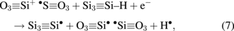
The obtained NBTI effects (as can be seen in Figs. 8–11) in the performed experiments are different, so it is logical to propose different responsible mechanisms. Thus, the buildup of Not (positive charged oxide traps) under the high negative oxide field at elevated temperatures during the NBT stress, presented in Fig. 8(a) (NBT-RAD experiment), can be attributed to hole trapping at oxygen vacancy defects30) and at dangling Si–H bonds near the SiO2–Si interface:


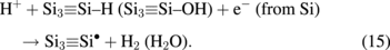
The buildup of Nit during the NBT stress, presented in Fig. 9(a) (NBT-RAD experiment), can also be ascribed to mutual influence of high electric field and increased temperature when Si–H bonds at the SiO2–Si interface can dissociate:7)

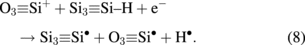
Released hydrogen atoms are highly reactive and they also can dissociate the interfacial Si–H bonds, thus leading to additional creation of interface traps:7,9,58)

Note that the reactions between H• atoms and holes from the substrate are also possible:58)

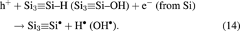
Formed H+ ions, which are drifting away from the interface under the negative oxide field, can dissociate the Si–H bonds in the gate oxide near the interface:7,58)

In this way hydrogen ions can additionally contribute to increase of Not. It should be emphasized that above reactions (3)–(6) can also occur in the opposite direction.
The trapped positive charge gradually decreases local electric field in the vicinity of SiO2–Si interface, leading to slower buildup of Not as the stress time increases. Also, the trapped oxide charge may be transformed into the interface traps in the later phase of NBT stress:30)
On the other hand, two mechanisms might be responsible for the effects observed during the NBT stressing after irradiation (RAD-NBT experiment) presented in Figs. 10(b) and 11(b). The first one is the activation of electrochemical reactions contributing to NBTI, which leads to additional creation of oxide charge and interface traps, and another is annealing/transformation of irradiation-induced oxide charge due to high temperature (175 °C) applied. The density of defects induced during irradiation at zero gate bias was rather small. That is why the number of available defect precursors remained rather high, so the subsequent NBT stress in this case has been dominantly accompanied by additional defect creation (the final values of Not and Nit densities are somewhat higher than their initial values during NBT stress, which indicates that mechanisms responsible for NBT instabilities — reactions 1–6 are dominant). In general, the observed effects of NBT on Not and Nit during these conditions are similar to behaviours during NBT stress of virgin devices. However, some decrease of Not could be observed after one hour of NBT stress, indicating the more pronounced transformation mechanisms of Not and Nit. On the other hand, irradiation with gate bias applied produced much higher density of defects (slightly more pronounced in the case of VG = +10 V than in the case of VG = −10 V). Hence, the annealing/transformation of these defects was actually dominant over the new defect creation during the subsequent NBT stress, thus leading to significantly lower Not at the end of stress than that at its beginning. A slight simultaneous increase of Nit is the consequence of transformation of Not in Nit.
The final value of Not after annealing is smaller in RAD-NBT experiment (with gate bias applied) than that in NBT-RAD experiment [Figs. 8(c) and 10(c)]. The reason for observed effect is Not decrease during NBT stress [Fig. 10(b)], which also leads to smaller annealing rate in this case.
It should be emphasized that the presented results obtained during NBT stressing of power VDMOSFETs represent mostly permanent (non recoverable) component and perhaps only the slowest part of the recoverable component of NBT stress induced degradation.6,36) Namely, due to delay time for measurement we generally refrain ourselves from discussing the quickly recoverable component of degradation and only consider cummulative data, mostly related to the permanent component and slow component of degradation that does not recover so quickly.
4.2. Irradiation
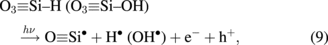
Regarding different behaviour of Not [Figs. 8(a) and 10(a)] and Nit [Figs. 9(a) and 11(a)] in irradiated and NBT stressed devices, it must be emphasized that the mechanisms occurring during irradiation are in fact different from those occurring during NBT stress, although the number of related electro-chemical reactions involving hydrogen species and holes seem almost the same. The well known consequence of reactions occurring during the irradiation is the buildup of Not and Nit, which can be seen in Figs. 10(a) and 11(a) (RAD-NBT experiment), as well as in Figs. 8(b) and 9(b) (NBT-RAD experiment). Namely, a high energy gamma-radiation (MeV in magnitude) breaks not only the weak Si–H and Si–OH bonds in the oxide, but also the regular Si–O–Si bonds:

During irradiation, the part of the created e−–h+ pairs can be recombined, so the broken atomic bonds can be reestablished.3) Also, covalent atomic bonds in the oxide can be broken by electrons that escaped the recombination, the process being more dominant than breaking the bonds by radiation.21) Thus, new e−–h+ pairs can be formed. The electrons will be almost immediately removed through the gate (within picoseconds39)) in the case of VG = +10 V. On the other hand, in the case of VG = −10 V electrons will be removed through the semiconductor (bulk is internally connected to source, which is grounded during irradiation).
The holes move toward the SiO2–Si interface, supported by the local electric field in the case of no bias applied or by both local and external electric fields in the case of positive gate bias applied. The holes arriving near the SiO2–Si interface react with numerous trap precursors, leading to Not increase:

Considering that the holes are trapped very close to the top of oxide valence band, the probability of their excitation into the oxide valence band is very high:

A fraction of the holes may dissociate weak Si–H and Si–OH bonds and can be trapped again in the oxide contributing to Not increase:

Another fraction of the holes could be trapped at oxide defects, such as oxygen vacancies, also contributing to Not increase by a reaction identical to (1). Note that holes in this case can also react with hydrogen atoms forming the ions [reaction (5)]. These hydrogen ions also could contribute to the oxide trapped charge increase.58) Released holes can dissociate weak Si3≡Si–H and Si3≡Si–OH bonds at the interface creating interface traps:
Similarly, hydrogen ions can also contribute to creation of interface traps:
It is obvious that irradiation under the gate bias applied in both experiments (NBT-RAD and RAD-NBT) leads to significantly higher increase of Not and Nit (somewhat higher in the case of VG = +10 V than in the case of VG = −10 V), then irradiation without gate bias applied. These results are in good agreement with the results of low-dose bias irradiation experiment (up to 150 Gy at ±9 V), by Johnson et al., performed on power p-channel DMOS devices at cryogenic temperatures.59) The reason for these differences is found in electric-field dependence of radiation effects.39) The higher the electric field, the more unrecombined holes remain trapped on O3≡Si• •Si≡O3 defects.
In addition, a small difference between effects of irradiation with +10 and −10 V gate bias can be explained by small difference between the corresponding values of electric field in the oxide, which affects the removal of electrons. Namely, the value of oxide electric field is somewhat higher in the case of positive gate bias (accumulation) than in the case of negative gate bias (strong inversion) because the difference in surface potential is about 0.8 V, so the irradiation effects at positive gate bias are somewhat more pronounced. A small positive electric field exists in the oxide as a consequence of small work-function difference between the poly-Si gate and n-bulk of pMOSFET, even in the case of zero bias. Because the fractional yield of holes for Co-60 source is very sensitive at lower electric fields,60) radiation response is evident even in the case of VG = 0 V.
Positive electric field in the oxide, not only efficiently separates generated carriers, but also forces the motion of positive gate oxide charge toward the interface (SiO2–Si) over the hole hopping process,61) while negative electric field forces their motion toward the gate. Small difference in radiation responses between devices irradiated at VG = +10 and −10 V suggests that gate oxide charge has not been moved deeper into the oxide by negative electric field.
Also, the final values of Not and Nit after irradiation of previously NBT stressed devices are significantly higher than values of Not and Nit after irradiation of virgin devices. However, the rates of radiation-induced increase of both Not and Nit is somewhat lower in the case of previously NBT stressed devices, and the reason is found in reduced number of defect precursors after NBT stress.
4.3. Annealing
Annealing step has been only thermally supported (without gate bias), so the observed decrease trend of Not and Nit values during annealing in both experiments [Figs. 8(c)–11(c)] might be in conjunction with diffusion of hydrogen molecules from the areas of high concentrations in oxide toward lower concentrations near the interface. The hydrogen molecules can be cracked not only at charged O3≡Si+ oxide traps by the reverse reaction (6), but also at O3≡Si+ •Si≡O3 by the reaction:

The result of these reactions is neutralization of positive oxide traps accompanied by the release of H+ ions.62)
The decrease of Nit during the annealing might be also attributed to the hydrogen species (molecule H2 and highly reactive atom H•) involved in reverse reactions (3) and (4).63) These reactions have obviously resulted in interface traps passivation.
Described mechanisms are reflected in the above changes of Not and Nit, which have caused the threshold voltage changes [Figs. 2(c) and 3(c)]. These results are in agreement with comparable published results, and they also correspond to so-called HDL model in interpreting irradiation effects and later in NBTI phenomena.64) The noticed change in tendency direction from decrease of Nit (RAD-NBT experiment) to increase (after more than 100 h of annealing) is quite possible to ascribe to border traps associated with hydrogen near the interface.58) The obtained results are also in excellent agreement with results regarding annealing of p-channel DMOS devices which have been low-dose bias irradiated at cryogenic temperatures.59)
5. Conclusions
The results of consecutive irradiation, bias temperature stresses, and annealing of p-channel power VDMOSFETs have been reported in this paper. The purpose of this research has been to examine the specific stress effects in devices which previously have been subjected to the other stress. The results have shown that irradiation of previously NBT stressed devices activates the mechanisms of additional defect creation in the oxide and at the interface, leading to further increase of threshold voltage shift. On the other hand, NBT stress in previously irradiated devices has lead to different effects, depending on the irradiation conditions. In the case of irradiation with low irradiation doses or without gate bias, NBT stress has led to further device degradation indicating that mechanisms responsible for additional creation of oxide trapped charge and interface traps are dominant in the initial period of NBT stress. It is interesting that, under these conditions, mechanisms responsible for transformation of oxide trapped charge into interface traps are activated after one hour of NBT stress leading to slight decrease of Not. These mechanisms are more pronounced in the case of gate bias applied. Namely, in the case of irradiation with gate bias, NBT stress has led to gate oxide charge decrease and interface trap increase, indicating that mechanisms responsible for transformation are dominant. In this case, NBT stress practically had a positive role because that it annealed a part of irradiation-induced degradation.
Acknowledgements
This research was supported by the Ministry of Education, Science and Technological Development of the Republic of Serbia under Grants Nos. OI171026 and TR32026, and by Serbian Academy of Sciences and Arts (SASA) under the Grant No. F-148. Also, the authors would like to thank the staff of Metrological Laboratory for Radiation Protection and Dosimetry at the Institute for Nuclear Sciences, Vinča, Serbia, for providing the facilities for radiation experiments.