
Abstract
During the past quarter century, the development of nanoscience and nanotechnology has been very much influenced and substantiated by the emergence of real nanometer-scale materials headed by fullerenes, carbon nanotubes (CNTs), and graphene, the so-called nanocarbons. This review article deals with some of the recent progress in the syntheses, characterization, and applications of the hybrid materials composed of nanopeapods (CNTs encapsulating atoms, molecules, nanowires, and nanoribbons). All of these studies are closely related to the characteristic usages of the internal nanospace prepared by the CNTs. Furthermore, the two-dimensional (2D) space prepared by two sheets of graphene has also been used as a 2D template for observing some dynamical phenomena of liquidus materials by transmission electron microscopy even under high-vacuum conditions.
Export citation and abstract BibTeX RIS
1. Introduction
One of the most salient features of the so-called nanocarbons (i.e., fullerenes, carbon nanotubes, and graphene)1) is their ability to encapsulate atoms, molecules, nanowires, or even nanoribbons in their internal hollow space. These nanospaces are very special in terms of the zero-, one-, and two-dimensionalities generated by the nanocarbons.
Upon the encapsulation of metal atom(s), the electronic and magnetic properties of fullerenes, for example, vary drastically depending on the number of atoms and/or the kind of atoms encapsulated, where electron transfers from the metal atom(s) to the fullerene cages play a crucial role in the property changes.2–5) Similar electron transfers occur in single-wall carbon nanotubes (SWCNTs) encapsulating metal nanowires; for example, semiconducting SWCNTs become metallic SWCNTs upon the encapsulation of metal nanowires owing to the electron doping from the nanowires to the SWCNTs.6,7)
The inner hollow spaces of SWCNTs or double-wall carbon nanotubes (DWCNTs) are especially interesting as one-dimensional nanometer-scale reaction vessels. One such example is the transformation from C60-encapsulating SWCNTs (the so-called peapods) to DWCNTs, where C60 molecules inside the nanotubes fuse together to form carbon nanotubes when the C60 peapods are annealed at 1,200 °C for two days.8) Single-wall boron nitride tubes (SWBNTs), which are normally very difficult to synthesize using the conventional synthetic methods, can easily be fabricated within SWCNTs when ammonia borane (H3NBH3) peapods are annealed at a high temperature as with C60 peapods.9) Even sp3 "diamond nanowires" are produced when diamondoid (such as adamantane and diamantane) peapods are treated at high temperatures.10) The formation of diamond nanowires has never been observed in the conventional bulk syntheses. All of these examples indicate that the inner space of CNTs is unique in synthesizing novel nanomaterials.
In this review article, after a brief historical introduction, recent progress in the fabrication, characterization, and applications of new hybrid nanomaterials prepared within the hollow space of CNTs is presented and discussed with a strong emphasis on materials science points of view. Also, the usages of two-dimensional space/templates prepared by two sheets of single-layer graphene for the observation of dynamical aspects of liquidus materials by electron microscopy are presented and discussed.
2. 1998 MRS Fall Meeting in Boston
David Luzzi of the University of Pennsylvania (U Penn) was in front of his poster at the 1998 MRS Fall Meeting, which was held from November 30th to December 3rd in Boston, telling the poster audience that C60 fullerene molecules could be encapsulated in SWCNTs under the title of "Synthesis of C60 Chains Contained within Carbon Nanotubes".11) He showed a very intriguing transmission electron microscopy (TEM) image (Fig. 1)11,12) in which one-dimensionally aligned spherical "balls" were seen within the SWCNT, and he claimed that these balls should be C60 molecules judging from their size and shape. According to Luzzi, the C60 molecules had accidentally crept into the inner space of the SWCNT during the sample preparation needed for TEM observations.
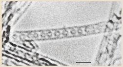
Fig. 1. Single-wall carbon nanotube containing a row of closed carbon shells concentric with the tubule axis. The diameter and center-to-center spacing of the internal shells are consistent with a chain of C60 molecules. The nanotube is surrounded by a vacuum. Scale bar = 2 nm. Reprinted with permission from Macmillan Publishing Ltd. © 1998. Rights managed by Nature Publishing Group.
Download figure:
Standard image High-resolution imageI was attending this Meeting as an invited speaker for a symposium entitled "Carbon Nanotubes, Fullerenes and Related Carbon Materials". In fact, I was very puzzled by the way he talked because, although the TEM image was very interesting and thought-provoking, it was not entirely evident that C60 molecules were safely "encapsulated" within the SWCNT. They might have been "on" the SWCNT and might not necessarily have been within the SWCNT since this was a "transmission" electron microscopy image.
Surprisingly, Sumio Iijima of Meijo University was already in front of Luzzi when I came close to Luzzi's poster, asking questions in rapid succession to Luzzi. Iijima was also attending the Meeting as a keynote speaker for the symposium. One of the Iijima's main concerns was, of course, the interpretation of the TEM image. Although Luzzi's corresponding less-than-one-page paper had just been published in Nature9) a week before the Meeting, he did not have any additional supporting TEM images similar to the one he used in the Nature paper. He said that this had been an accidental observation/discovery and he did not know how to synthesize high yields of this unique hybrid material of an SWCNT and C60 fullerene. This carbon nanotube-fullerene hybrid was soon named the "peapod" by Jack Fisher at U Penn, which actually has been well accepted and used by the scientific community to date.13)
Even though I was half in doubt about the existence of the peapod, I thought this might be a brand-new series of carbon nanotubes if they truly existed. Unfortunately, however, I had no idea at that time of any specific method of synthesizing this fascinating peapod.
3. High-yield peapod synthesis
A couple of years after the first report of the peapod by Luzzi, an easy and straightforward synthesis of the peapod was independently reported by two Japanese research groups, Shunji Bandow at Meijo University8) and Hiromichi Kataura then at Tokyo Metropolitan University.14) To my great surprise, according to them, all one had to do to synthesize the peapod was to prepare cap-opened SWCNTs and C60 powder, which were mixed and vacuum-sealed in a glass ampoule and heated in a high-temperature oven at 1,200 °C for 48 h. At this high temperature, C60 molecules sublime at a certain vapor pressure whereas the SWCNTs remain as they are at room temperature (Fig. 2). Interestingly, if the diameter of the SWCNTs used is slightly larger than that of C60, C60 molecules are observed to be encapsulated in the SWCNTs in a perfect one-dimensional fashion.

Fig. 2. Probable growth mechanism of C60@SWCNT peapods. C60 molecules sublime under vacuum conditions at temperatures above 450 °C and self-assemble in the inner space of the SWCNT.
Download figure:
Standard image High-resolution imageMoreover, the yield of the peapods is very high, normally as high as 80–90%.11) This is an easy and self-assembled process because theoretical studies15,16) predict that the stabilization energy of C60 is much higher for the peapod than for the C60 molecules situated outside the SWCNTs. Importantly, the discovery of this easy synthesis of the C60-peapod opened an entirely new field of carbon nanotube materials research.
4. Metallofullerene peapods
Not only C60 but also other fullerenes such as metallofullerenes can be encapsulated in SWCNTs in a similar fashion if they are of suitable size.17,18) In fact, some of the most interesting peapods are the so-called metallofullerene peapods where metallofullerenes [fullerenes containing metal atom(s)] are encapsulated in SWCNTs, because the interaction between metallofullerenes and SWCNTs should be much stronger than that between C60 molecules and SWCNTs owing to charge transfer from the metallofullerenes to the SWCNT.
Figure 3 shows the first high-resolution TEM (HRTEM) images of the aligned Gd@C82 chains encapsulated in SWNTs.17) The diameter of the SWNTs that contain these metallofullerenes ranges from 1.4 to 1.5 nm. The dark spots seen on most of the C82 molecules correspond to the Gd atoms in the metallofullerene cages. Such dark spots have never been observed in HRTEM images of empty C60 molecules. The experiment truly demonstrates that the fullerene contains a single metal atom inside each cage. The Gd atoms are off center in each C82 molecule, which is a common characteristic for metallofullerenes.2–5) Being able to see the metal atoms means that the fullerene cages are not spinning even at room temperature. However, missing dark spots imply that some of the cages are spinning. The nanotubes used in this experiment frequently form bundles with an average intertubule spacing of 1.89 nm. Very interestingly, the encapsulation yield of Gd@C82 is much higher than that of C60@SWCNT because of the stronger interaction between (Gd@C82)@SWCNT and SWCNTs.
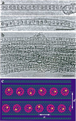
Fig. 3. (a, b) HRTEM images of the isolated and bundled SWCNTs containing Gd@C82 fullerenes. Dark spots seen on most of the fullerene cages correspond to the encapsulated Gd atoms that are oriented randomly with respect to the tube axis (scale bar = 5 nm). (c) Schematic representation of the metallofullerene containing SWNTs: (Gd@C82)n@SWCNTs. Reproduced with permission from Ref. 17. © 2000 American Physical Society.
Download figure:
Standard image High-resolution imageOne of the important consequences of the observed interaction between Gd@C82 and SWCNT is the ambipolar characteristic of the field-effect transistors (FETs) that use Gd@C82@SWCNT as a channel.19,20) The FET circuits were fabricated on a SiO2 insulating layer (100 nm) on top of a heavily doped silicon substrate. Source and drain electrodes were formed by electron beam lithography, metal evaporation (Ti/Au: 3/15 nm), and lift-off processes. The gap between source and drain electrodes was 400 nm. A heavily doped Si substrate was used as a backgate. The backgate electrode was prepared by metal evaporation (Ti/Au: 100/300 nm). The Gd@C82@SWCNT peapods were dispersed in 1,2-dichloroethane solutions and added dropwise to the substrate.19)
The ID–VGS characteristics of a Gd@C82-peapods-FET are shown in Fig. 4.19) Starting from a positive gate voltage VGS, the current ID decreases steeply by three orders of magnitude towards 0 V and then gradually increases. This indicates that Gd@C82 peapods exhibit ambipolar FET behavior with both n and p channels easily accessible by simple electrostatic gates. Such ambipolar behavior was not observed in C60 peapods. The origin of the observed ambipolar behavior is closely related to the electronic structure of Gd@C82 peapods.

Fig. 4. ID–VGS curve for Gd@C82 metallofullerene peapods (VDS = 20 mV). The inset is an AFM image of the Gd@C82 peapods-FET used in the measurement. Reproduced from Ref. 19.
Download figure:
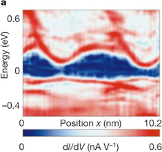
Standard image High-resolution imageThe electronic properties of Gd@C82@SWCNT peapods are very interesting owing to the strong charge transfer from Gd@C82 to SWCNTs. To obtain further information on peapod electronic properties, we conducted low-temperature scanning tunneling microscopy (STM) and scanning tunneling spectroscopy (STS) on a Gd@C82@SWCNT.21) Figure 5(a) shows the spatial variation of dI/dV spectra along a Gd@C82@SWCNT. The chirality of the Gd@C82@SWCNT was determined to be  from the measured diameter of 1.4 nm (nominally 1.375 nm) with a chiral angle of 27° (nominally 26.7°). In the dI/dV spectra, conduction and valence band edges are also visible with two smaller van Hove singularity peaks at higher bias voltages. The original bandgap of 0.43 eV narrows to 0.17 eV at the site where the Gd@C82 is located (the bandgap modulation). At other locations along the peapod axis, we observed a modified conduction band with a different shape as shown in Fig. 5(b). Various shapes of the modified energy band reflect variations in local elastic strain and/or energy transfer.
Download figure:
Standard image High-resolution image
Fig. 5. Bandgap modulation of a Gd@C82@SWCNT peapod by encapsulated Gd@C82. (a) dI/dV spectra taken along the Gd@C82@SWCNT. The x-axis represents the position along the Gd@C82@SWCNT. The y-axis represents the energy, and the color scale the local density of states. (b) Topographic image of a  Gd@C82@SWCNT at a sample bias voltage of 0.5 V. The sites of inserted Gd@C82 are indicated by arrows (bottom); the corresponding dI/dV spectra of the conduction band at the center of the Gd@C82@SWCNT are also shown (top). Reprinted with permission from Macmillan Publishing Ltd. © 2000. Rights managed by Nature Publishing Group.
Download figure:
Standard image High-resolution imageThere are several causes that could account for the change in the bandgap. A charge transfer from the metallofullerene to the SWCNT induces a modulation in the electronic structure. It is also possible that mechanical deformation of the SWCNT due to the encapsulation of Gd@C82 may induce the modulation. The greatest effect of this mechanism is to shift the entire STS spectrum (both conduction and valence bands), as well as contributing to the bandgap modulation. We noticed that the Fermi level was close to the valence band edge owing to the charge transfer and that the majority of the modulation occurs in the conduction band.6,21)
5. Metal-nanowire peapods
The inner space of SWCNTs is unique and very special as we have seen above. By using this inner space, one may induce unusual reactions that have not been observed in the normal bulk state. One of the best examples of this is the transformation of metallofullerene peapods to double-wall CNTs (DWCNTs) encapsulating metal nanowires.22)
Figure 6 schematically shows the transformation of Gd metallofullerenes into Gd nanowires encapsulated in SWCNTs within the outer SWCNTs.22) In an earlier study, the transformation of C60@SWCNTs into DWCNTs was reported by Bandow et al.8) when C60@SWCNTs were annealed at 1,200 °C for 48 h. In the case of Gd metallofullerenes, linearly aligned Gd nanowires were also observed in DWCNTs, suggesting that Gd atoms in C82 fused together very efficiently to form the Gd nanowires in the DWCNTs. This never happens in the bulk state.
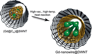
Fig. 6. Schematic representation of the formation of Gd nanowire via nanotemplate reaction on metallofullerene peapods. In the figure, the green balls represent gadolinium atoms, the gray sticks represent carbon atoms of the outer CNT, and the yellow sticks represent carbon atoms of the inner CNT. Reproduced with permission from Ref. 22. © 2008 American Chemical Society.
Download figure:
Standard image High-resolution imageHRTEM observations of the Gd nanowires in DWCNTs reveal that Gd atoms are located at the corners of a square with a Gd–Gd distance of 0.40 nm, and the squares are spaced at an average interval of 0.43 nm. The length of this nanowire structure estimated from the HRTEM image is ca. 60 nm, and, therefore, the number of encapsulated Gd atoms is estimated to be ca. 560. This number is a reasonable value, because 560 Gd@C82 molecules packed closely in the CNTs correspond to a length of 0.6 µm, which is appropriate for the length of CNTs used in this experiment.
In fact, several studies on the formation of nanoclusters and nanowires in CNTs have been reported over the past couple of decades.23,24) However, the high-yield formation of atomically thin nanowires inside CNTs has been difficult to date. Although the above-mentioned method to fabricate nanowires encapsulating SWCNTs is interesting, a more direct and efficient way to synthesize these novel CNT materials is the so-called vacuum sublimation method,25) in which ultrathin nanowires of typically 1–4 atomic chains are synthesized with a high filling fraction (typically >80%) in both SWCNTs and DWCNTs. These nanowires are completely protected by the surrounding walls of the CNTs and are therefore free from oxidation and structural decomposition under ambient (air) environments and even after ultrasonication in solution. This is in marked contrast to previously reported metal nanowires, especially the single atomic nanowires, which can survive for only a very short period of time even under ultrahigh-vacuum conditions.26,27) Furthermore, the present method of preparing ultrathin metal nanowires in CNTs can be applied to any metal atoms that have low sublimation temperatures.
Metal nanowires were synthesized by placing high-quality purified SWCNTs and metal powder into a glass tube under vacuum (10−6 Torr) with heating. At a high vacuum and high temperature, metals with low sublimation temperatures can vaporize to form atomically thin nanowires in the nanosize pseudo-1D space of CNTs. Using this simple procedure, which we call the direct nanofilling reaction, we synthesized various ultrathin metal nanowires in CNTs. For example, we focused on Eu metal because of its low sublimation temperature and unique magnetic properties arising from partially filled 4f orbitals.
Figures 7(a)–7(c) show HRTEM images and a schematic presentation of Eu nanowires synthesized by using DWCNTs with an inner diameter of 0.7 nm.25) This process allows the ultrathin atomic Eu nanowires to retain their original structure even after ultrasonication for 1 h. Furthermore, almost identical HRTEM images to those of the as-produced Eu nanowires were observed even after exposure of the sample to air for one month. The remarkable stability of the nanowires originating from the perfect protection afforded by the CNT walls is one of the most important advantages that led us to investigate their properties in detail and further fabrication methods for device applications. Interestingly, the interatomic distance between neighboring Eu atoms determined by direct lattice measurements was found to be 0.467 nm with a standard deviation of 0.019 nm, which is much larger than that of the bulk Eu crystal (0.39681 nm). The observed large Eu–Eu distance in the single-chain atomic wire corresponds to an elongation of approximately 17% relative to that of bulk crystal, which presumably originates from a significant reduction of the coordination number of Eu atoms (from 12 to 2) and from a possible charge transfer interaction between Eu atoms and CNTs.

Fig. 7. (a) HRTEM image of a single-atomic chain of Eu encapsulated in DWCNTs. (b) Magnified HRTEM image and HRTEM image simulated by a multislice method at the Scherzer defocus. (c) Structure model of observed HRTEM image represented by a ball-and-stick model and space-filling model. The left and right pictures show the structure model perpendicular and parallel to the tube axis, respectively. Gray represents carbon and green represents europium. All image simulations were performed using the WinHREM simulation software package. Reproduced with permission from Ref. 25. © 2009 Wiley-VCH Verlag GmbH & KGaA.
Download figure:
Standard image High-resolution imageThe magnetic property of Eu-nanowires@SWCNTs is especially interesting when compared with those of the intact SWCNTs and bulk Eu, and it is a result of the unique nanowire structures observed by HRTEM. Figure 8 shows the temperature dependence of the magnetic susceptibility of purified open-capped SWCNTs, Eu bulk crystal, and Eu-nanowire@SWCNTs with a mean diameter of 1.7 nm measured at a magnetic field of 1.2 T. The magnetic susceptibility of purified open-capped SWCNTs is very low, and hence we can ignore background magnetization arising from SWCNTs.25)
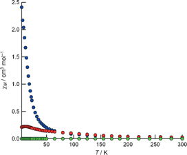
Fig. 8. Temperature dependence of the magnetic susceptibility of bulk Eu crystal, Eu-nanowire@SWCNTs, and purified open-capped SWCNTs. Blue, Eu nanowire@SWCNTs; red, bulk Eu crystal; green, purified cap-opened SWCNTs. Reproduced with permission from Ref. 25. © 2009 Wiley-VCH Verlag GmbH & KGaA.
Download figure:
Standard image High-resolution imageThe magnetization behavior of Eu nanowires is vastly different from that of Eu bulk crystals, especially below 50 K. The magnetic susceptibility of Eu nanowires is more than 10 times larger than that of the bulk Eu crystal at 4.25 K. In the case of Eu, the partially filled 4f orbital (the corresponding electronic configuration of Eu is 8S7/2) is the origin of the magnetic moment. As the 4f orbital is strongly localized, the magnetic properties of Eu compounds have been well described as a localized spin system, in which interspin interactions are mediated by free electrons (RKKY interactions). In the case of the bulk crystal of Eu metal, helical spin ordering is observed below 90 K, where all spins in the ab plane align in the same direction, and the spin direction in the ab plane rotates along the c-axis.
This helical spin ordering causes each spin alignment in the ab plane to cancel out, which leads to a decrease in the total magnetic moment. Because the structure and dimensionality of Eu nanowires are vastly different from those of the bulk Eu crystal, the helical spin alignment observed in the bulk Eu crystal is probably not present in Eu nanowires. Therefore, the cancelling out of spin observed in the Eu bulk crystal is also not present in Eu nanowires, which leads to a dramatic increase in the total magnetic moment. As described above, we can change not only the electronic structure but also the magnetic properties by changing the dimensions of the Eu metal.
6. Extraction of inner CNTs from double-wall CNTs
"Extraction" of the nanomaterials produced within CNTs is another important issue when one tries to characterize these nanomaterials outside the CNTs. Actually, this can be done beautifully in the case of DWCNTs by using the solution phase extraction method.28)
We found an efficient method to separate the inner and outer walls of the DWCNTs using ultrasonication and ultracentrifugation processes.28) The extraction of the inner walls is achieved by cutting the DWCNTs with vigorous sonication in water containing surfactants. The extracted walls produced in this manner are perfectly isolated SWCNTs encapsulated by surfactants and can readily be separated by using density gradient ultracentrifugation (DGU), which has been applied in the sorting of CNTs by diameter, chirality, and shell number (type) of CNTs. This finding provides an effective way of producing novel SWCNTs that have very small or large diameters, impurity free surfaces, and perfectly isolated states.28–30)
Figure 9 shows typical HRTEM images of CNTs observed in the DWCNT sample before and after the sonication.28) In the pristine DWCNT sample, the ratio of SWCNTs to DWCNTs was less than ca. 5%. The ratio of SWCNTs, however, drastically increased to 50% after the sonication. The extraction may well have resulted from the partial cutting of outer shells of DWCNTs at the time of sonication, which is followed by the mutual sliding of inner and outer shells. This sliding can be accelerated by the shock waves formed during the sonication. It is well known that the sonication treatment can cause the shortening and cutting of CNTs. An image of this partial cutting has actually been obtained for the MWCNTs by HRTEM observations. This technique may also provide opportunities to extract ultranarrow SWCNTs embedded in other supporting materials such as zeolites.31,32)
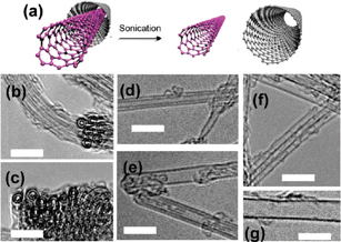
Fig. 9. (a) Schematic illustration of the separation of inner and outer shells in DWCNTs. Typical HRTEM images of DWCNT samples (b, c) before and (d–g) after the sonication treatment. The scale bar is 5 nm. Reproduced with permission from Ref. 28. © 2010 American Chemical Society.
Download figure:
Standard image High-resolution image7. Nanodiamond-nanowire peapods
One of the most important properties of the so-called nanocarbons (i.e., fullerenes, CNTs, and graphene) is their "aromaticity", in which sp2 carbon bonds play a dominant role in the electronic properties as well as the structures. Carbon atoms, however, also form sp3 bonds, which are typically represented by diamond. If the smallest diamond unit, adamantane, is encapsulated in SWCNTs, the peapods produced might exhibit some interesting structural and electronic properties. These were the first sp2–sp3 hybrid nanocarbon materials produced.
In fact, a variety of sp3 nanodiamond nanostructures have been discovered during the past decade.33) Adamantane, the simplest sp3 diamondoid, has long been known. Interestingly, the larger diamondoids were first isolated from petroleum only about a decade ago. The growth of diamond from such nanodiamonds has only just recently been achieved. The synthesis of diamond wires with diameters of 50–100 nm has been achieved, but the preparation of diamond nanowires with sub-nanometer diameters has not been achieved so far.
Diamondoids34,35) have been found to have strong affinity towards compatible host structures, such as cyclodextrins and CNTs. Analogous to the fabrication of sp2 CNTs from sp2 fullerenes, diamondoids may also fuse and transform into sp3 diamond nanowires. The templated growth of these nanowires from diamondoid assemblies confined in CNTs provides a probable pathway through a "face-fused" reaction.8,36,37) The fusion reaction of adamantane into diamond nanowires has been shown to be energetically unfavorable. However, under a hydrogen atmosphere at high temperatures, diamantane (the second smallest diamondoid molecule) can form a nanowire structure. We found, by TEM observation, a diamond nanowire inside a DWCNT, which is shown in Fig. 10.37) The simulated TEM image in the figure is consistent with the observed image. Comparing the simulated TEM images of the different candidate structures, we conclude that Fig. 10(a) most likely represents a nanowire with the (110) face. The TEM observation supports our conjecture that a CNT can provide an ideal environment for chemical reactions that are almost impossible in conventional bulk chemistry.
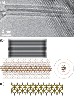
Fig. 10. (a) HRTEM image of a carbon-based nanowire inside a DWCNT; (b) simulated image of a diamond nanowire inside a DWCNT along with the corresponding structural model; (c) structural model of a diamond nanowire. Reproduced with permission from Ref. 37. © 2013 Wiley-VCH Verlag GmbH & KGaA.
Download figure:
Standard image High-resolution imageInterestingly, diamantane molecules also form one-dimensional (1D) linear-chain polymers in DWCNTs. One of the promising strategies for creating linear-chain nanodiamond polymers relies on the vapor-phase reaction of an apically dibromo-substituted diamantane, 4,9-dibromodiamantane, in the presence of hollow SWCNTs or DWCNTs.38) At a high vacuum and temperature (175 °C, 10−7 Torr), dibromodiamantane can be vaporized to form polymer chains inside the CNTs. An HRTEM image of the as-produced samples is shown in Fig. 11.
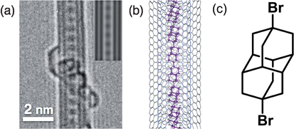
Fig. 11. (a) High-magnification TEM image of an as-produced sample; inset: simulated TEM image of a diamantane nanodiamond polymer confined in a DWCNT. (b) Corresponding structural model. (c) Molecular structure of 4,9-dibromodiamantane. Reproduced with permission from Ref. 38. © 2015 Wiley-VCH Verlag GmbH & KGaA.
Download figure:
Standard image High-resolution imageWell-aligned dots are observed in DWCNTs with relatively thin inner tubes [Fig. 11(a)].38) A close inspection of the space between individual dots reveals that the center-to-center distance d is 0.635 nm, which is in excellent agreement with density functional theory (DFT) computations at the B3LYP (D3BJ)/cc-pVDZ level of theory (d = 0.634 nm), which we carried out in parallel with the TEM studies. The monomer separation was evaluated for the nanodiamond polymer as depicted in Fig. 11(b), in which two diamantane skeletons are linked between their apical bridgehead positions through covalent bonds between sp3 hybridized carbon atoms. The dispersion-bound dimer with d = 0.891 nm is incompatible with the much shorter interdot distance observed by TEM. Indeed, the simulated TEM image is in good agreement with the observed images [Fig. 11(a), inset]. These experimental and theoretical analyses indicate the formation of linear-chain diamantane polymers, whose structural features are distinctly different from those of an array of the precursor material.
We expect that the present template-based approach will provide access to a diverse range of novel one-dimensional polymers. In principle, the present technique is applicable to various dihalogen-substituted molecules. In fact, preliminary experiments indicate that the polymerization can also occur with other precursor molecules. The present synthetic method may offer a new strategy for the design and synthesis of one-dimensional nanomaterials with CNTs.
8. Graphene nanoribbon peapods
Fabricating and characterizing the so-called graphene nanoribbons (GNRs) are important and challenging areas to investigate since the bandgap of single-layer graphene increases as the width of the graphene decreases. Several methods of preparing GNRs have been reported during the past decade. One of the novel methods to do this is to use the inner space of CNTs, which should be very efficient for the production of the GNRs with 1–2 nm widths.
There have been several studies on the fabrication of GNRs in CNTs39–44) through the confined polymerization of polycyclic aromatic hydrocarbon molecules. In addition, the theoretical models41,43,45) have suggested that GNRs in CNTs form a helical conformation owing to the geometric constraints imposed by the outer tube. The geometric constraints are expected to restrict the chirality of the synthesized CNT. By carefully choosing the polycyclic aromatic hydrocarbon precursors, one can, therefore, foresee the controllable tuning of the chiralities synthesized. By the inner-shell extraction technique discussed above in the case of DWCNTs,28) the precise verification of the CNTs synthesized is also possible through photoluminescence (PL) measurements.
For the fabrication of GNRs in CNTs, coronene is one of the best precursor molecules because of its high filling yield in the SWCNTs and its high reactivity, in addition to its size. It can easily be turned into its dimeric form during the encapsulation process to give a mixture of dimers and other linearly condensed coronene oligomers, which can also be regarded as short GNRs (S-GNRs), inside the template nanotubes. The resulting samples are heated at 700 °C to induce further polymerization/fusion reactions that produce long GNRs (L-GNRs). The products obtained before and after annealing are termed S-GNR@SWCNTs and L-GNR@SWCNTs, respectively.43)
The transformation of S-GNR@SWCNTs into L-GNR@SWCNTs is schematically shown in Fig. 12(a) and visualized by TEM images in Figs. 12(b) and 12(c).43) Densely packed, segmented structures of coronene dimers and oligomers, which align themselves at the center cavity of the SWCNT [Fig. 12(b)-(i)], are converted into long, linear, chainlike structures [Fig. 12(b)-(ii)]. The structural details of the L-GNRs formed can be clearly seen from the images taken under aberration corrected HRTEM (cs-HRTEM) in Fig. 12(c). Intensive surface modification leads to the structure shown in Fig. 12(b)-(iii), where the resulting nanotubes are covered with amorphous impurities that probably formed as a consequence of the diazonium radical side reaction.
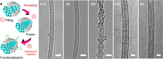
Fig. 12. (a) Overall reaction scheme, starting with (i) the introduction of coronene precursors into the template SWCNTs, followed by (ii) the coalescence of the molecules encapsulated, and finally, (iii) the surface modification of the outer sidewall by diazonium chemistry. (b) Corresponding HRTEM images of the products formed at each stage in (a). Scale bars = 2 nm. (c) Typical Cs-HRTEM images of the L-GNR@SWCNTs showing the (i) horizontal and (ii) perpendicular orientations of the inner GNRs. Scale bars = 1 nm. Reproduced with permission from Ref. 43. © 2015 American Chemical Society.
Download figure:
Standard image High-resolution imageA further reaction/conversion from GNRs to CNTs by thermal annealing is much more interesting. Indeed, we observed that the GNRs derived from a perylene derivative, perylene-3,4,9,10-tetracarboxylic dianhydride (PTCDA) (Fig. 13), are preferentially converted to  and
and  tubes in 1.4 nm outer tubes, providing strong evidence for an intertwining of both single and double strands of GNRs.43) This sheds light on the understanding of CNT growth, contributing not only to the future selective fabrication of GNRs but also to novel nanomaterial engineering.
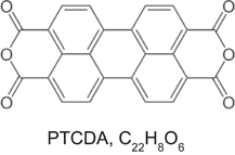
Fig. 13. Molecular structure of perylene-3,4,9,10-tetracarboxylic dianhydride (PTCDA).
Download figure:
Standard image High-resolution imageFigure 14 shows the growth and conversion mechanism of the GNRs produced from PTCDA via a twisted GNR and the final conversion into a CNT, all of which occur in a SWCNT.43) The precursors sublime and align into two linear arrays within the confined space of the host CNT. The oxygen atoms are released in the form of C and CO2 under mild heat treatment, yielding the radical species that subsequently polymerize into the GNRs. The thermally driven helical twisting of the GNRs accompanied by cyclodehydrogenation completes the transformation into the tubular structure under high-temperature annealing. Entangling of either a single- or double-helical perylene chain results in the formation of tubes bearing specific chirality as predicted from a two-dimensional honeycomb map [Fig. 14(a)].

Fig. 14. (a) Map of chiral vectors showing the possible  indices obtained from the intertwining of helical perylene chains. (b) Basic steps for the synthesis of CNTs via twisted GNRs, illustrated with stick model PTCDA monomers. Blue and white, carbon; yellow, oxygen; hydrogens are omitted for simplicity. The precursors align themselves inside the CNTs (omitted in the figure). Thermal treatment results in the removal of the heteroatoms as CO and CO2. Covalent interlinking of the radical intermediates results in the extended polyaromatic chains. The subsequent twist and cyclodehydrogenation lead to the assembly of a complete tubular structure with well-defined chirality. Reprinted with permission from Macmillan Publishing Ltd. © 2013. Rights managed by Nature Publishing Group.
Download figure:
Standard image High-resolution image9. Graphene analogue: 2D peapods
So far, we have discussed how some of the important peapod materials are fabricated in terms of the uniqueness of the inner space of CNTs. Indeed, several novel nanomaterials have been produced within CNTs that have not been synthesized under normal bulk conditions. This is because the inner space of CNTs is extremely small so only perfectly aligned one-dimensional materials can be formed within the inner space of CNTs.24)
Then a question arises as to whether or not a similar confined effect can be seen in the case of 2D graphene, that is, a confined space produced by two sheets of graphene. The most intriguing materials that can be prepared between two sheets of graphene are tiny liquid droplets, and the observation of these by TEM should provide some information regarding the dynamical aspects of the liquids. Observation of solutions using TEM can, in principle, provide direct information on the microstructure of a solution at the atomic level. Recent advancements in TEM have enabled us to observe the structure of matter with spatial and time resolutions of 0.05 nm and 1 ms, respectively. In addition, the development of low-acceleration voltage techniques has greatly expanded the versatility of TEM, enabling us to observe fragile bio-organic materials at atomic resolution. HRTEM simultaneously gives us information on electronic structure and bonding state. If TEM can be applied to observe solutions, it will be one of the most powerful characterization techniques to provide direct and high-resolution structural information on liquidus materials.46–48)
Traditionally, TEM observation of solutions has been achieved by using so-called environmental cells. Recently, we have demonstrated graphene liquid cells, i.e., liquids sandwiched by two single-layer graphene sheets, for the visualization of metal particles in solution with atomic resolution.49) Graphene is a one-atom-thick carbon sheet, and because it is the thinnest structure composed of a light element, graphene is almost transparent to an electron beam. In addition, graphene is a mechanically and chemically stable conductor as are CNTs, and high-contrast and stable TEM observation can be achieved using graphene as a sample support.50) In addition, even a single layer of graphene has perfect impermeability, and if a solution can be sandwiched between two graphene layers, the solution can be supported even under a UHV condition, which allows the TEM observation of the microstructure of the solution.49)
Figure 15 shows a schematic diagram of the preparation of a water-sandwiched cell using two sheets of single-layer graphene. First, a CVD-grown graphene sheet is transferred onto a SiN membrane grid that has 2 µm holes penetrating through the membrane. Second, using a mist generator, various solutions are sprayed onto another graphene sheet floating on an etching solution. Third, to form the graphene-sandwiched liquid cell, the deposited microsize solution droplets are covered with the graphene on the TEM grid. In the preparation of the graphene liquid cell, the use of large-area and seamless graphene sheets is essential to realize the successful encapsulation of solutions. To achieve high-yield preparation of the graphene liquid cell, we have developed a growth technique for high-quality large-area graphene layers by a chemical vapor deposition (CVD) method developed in the present laboratory.
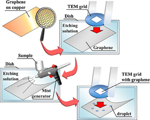
Fig. 15. Preparation scheme of the graphene-sandwiched structure. The graphene sheets can be observed by careful irradiation with suitable fluorescent light. Reproduced with permission from Ref. 49. © 2016 Elsevier.
Download figure:
Standard image High-resolution imageFigure 16 shows a typical TEM image of a graphene liquid cell using the CVD-grown large-area graphene, where a pure water droplet is used as the liquid encapsulated between the two single layers of graphene.49) The dark contrast region corresponds to the graphene water-sandwiched area with a typical lateral size of 160–300 nm. The estimated average thickness of the sandwiched region is 10–20 water molecule layers. In terms of EELS measurements, the oxygen peak of the droplets is very close to that of bulk water, indicating that the chemical environment around the oxygen atoms of the observed nanodroplets is very similar to that of bulk water. Black spots seen in the TEM image are due to Cu nanoparticle residue, which is formed and deposited during the transfer process.
Fig. 16. (a) Room-temperature typical TEM image of water droplets (dark contrast region) sandwiched by two sheets of single-layer graphene. The black spots are Cu nanoparticle residues, which are formed and deposited during the transfer process. (b) Electron diffraction pattern of graphene water-sandwiched area shown in (a). The twin hexagonal patterns show the graphene-sandwiched structure, which is made of two sheets of single-layer graphene. (c) Low-magnification typical TEM image of the graphene liquid cell. The SiN membrane, which has 2 µm holes, is found at the edge of (c). The many trigonal dark points shown in the water-encapsulated area correspond to holes in the membrane. Reproduced with permission from Ref. 49. © 2016 Elsevier.
Download figure:
Standard image High-resolution imageFigure 16(b) shows two sets of diffraction patterns with sixfold symmetry, which confirms the successful preparation of the graphene-sandwiched structure. The electron diffraction pattern shows diffraction spots originating only from the graphene layers and not from the water droplet, demonstrating the liquid state of the droplet. The relative angle of the two hexagonal patterns is about 5°, indicating that two graphene sheets with a relative angle of 5° stack to form the graphene-liquid cell. Relative angles in graphene liquid cells are found to vary from one sample to another owing to random stacking caused by the manual stacking procedure used in the current preparation method of graphene liquid cells.
Figure 16(c) shows a typical low-magnification TEM image of the graphene liquid cell.49) Approximately 35 small droplets are counted in each hole in the SiN membrane and almost 80% of the holes are suspended by bilayer graphene and the graphene liquid cells. Time-dependent TEM observation often shows the creation of bubbles within the water-sandwiched area caused by radiolysis by electron beam irradiation during the observation, which accompanies the decomposition of the droplets in a graphene pocket. Figure 17 shows a schematic presentation of the present water-sandwiched structure.
Fig. 17. Schematic of graphene water-sandwiched droplet structure.
Download figure:
Standard image High-resolution image
10. Conclusions and future perspective
This review has dealt with the growth, structures, and electronic and magnetic properties of the so-called peapods, which are known as a novel class of CNT-related materials. Using the inner space of CNTs allows the fabrication of brand-new nanomaterials encapsulating metallofullerenes (fullerenes with metal encapsulated), nanowires of metal or nanodiamond, graphene nanoribbons, and other novel nanomaterials. Furthermore, we show that the 2D space made by two sheets of single-layer graphene is an ideal 2D nanospace for encapsulating tiny droplets of liquidus materials such as water droplets, which can be visualized by transmission electron microscopy under ultrahigh-vacuum conditions.
One of the most important issues in nanopeapod research at the present time is that the new materials (nanowires, nanoribbons, etc.) fabricated within CNTs need to be extracted from the CNTs in order to obtain them as pure materials for characterization and applications. As described in the text, there has been some progress in this, but we are still only part of the way to finding a universal method to realize this, which is a challenging and important topic to pursue. In any case, nanopeapods will continue to tantalize physicists, chemists, and materials scientists for years to come.
Acknowledgments
I would like to express my thanks to present and past coworkers in my laboratory, Ryo Kitaura (Nagoya University), Haruka Omachi (Nagoya University), Yusuke Nakanishi (Nagoya University), Yasumitsu Miyata (Tokyo Metropolitan University), Toshiya Okazaki (AIST Tsukuba), and Toshiki Sugai (Toho University), together with many international and domestic collaborators for carrying out most of the peapod studies described in this review article. I must apologize for not mentioning them individually. I would like to thank the daily efforts of many graduate students and postdocs in my laboratory for their valuable help in advancing this research. This paper has been supported by MEXT/JSPS KAKENHI Grant Number JP16H06350.
Biographies

Hisanori Shinohara received his Ph.D. in Chemical Physics from Kyoto University in 1983. He obtained an assistant professorship at the Institute for Molecular Science (IMS) at Okazaki in 1979. He then became an associate professor in Materials Chemistry at Mie University in 1988. He came to Nagoya University in 1993 as a full professor in Physical Chemistry. He is the recipient of the Japan Chemical Society Award (2010), the Chunich Cultural Award (2011), the Japan Society of Applied Physics Outstanding Paper Award (2012), the Medal of Honor with Purple Ribbon (2016), and the Fellow of the Royal Society of Chemistry (FRSC) Award (2016). He is widely known for his achievements in the production and characterization of endohedral metallofullerenes and novel carbon nanotube materials including nanopeapods. In total, he has published over 560 original and peer-reviewed scientific papers including approximately 400 in top physics, chemistry, and materials science journals, as well as more than 50 review papers in journals and books.