

Abstract
Current-induced magnetization switching is demonstrated in a micron sized Hall bar consisting of Pt-capped ultrathin ferrimagnetic MnGa films. The films showed a low magnetization Ms ≃ 150 kA/m and a large perpendicular magnetic anisotropy (PMA) field  T, indicating a PMA thickness t product
  mJ/m2, which is relatively larger than those reported for other material films with PMA. Magnetization switching induced by an in-plane electrical current was examined with the application of an in-plane magnetic field. The phase diagram of the switching current vs the in-plane magnetic field is qualitatively consistent with that of the torque due to the spin-Hall effect in the Pt layer.
Export citation and abstract BibTeX RIS
The use of spin–orbit torque (SOT) has attracted much attention as one of the ways to electrically manipulate the magnetization of magnetic thin films by applying an electrical current.1–5) Many studies have been performed on SOT for magnetic films with in-plane and perpendicular magnetic anisotropy (PMA) from both fundamental and technological points of view. In particular, current-induced SOT switching of magnetization in films with PMA is technologically important, this is because it can be used as a writing technique for a three-terminal device utilizing a perpendicularly magnetized magnetic tunnel junction (p-MTJ), which can serve as a memory element of magnetoresistive random access memory (MRAM).6) The basic concept is similar to that of MRAM based on spin-transfer-torque (STT) writing7–9) or voltage-controlled magnetic anisotropy (VCMA) writing.10,11)
Most studies on SOT for PMA films have been performed on thin layered films with an interfacial PMA composed of a heavy metal, e.g., Ta, W, and Pt, and ultrathin ferromagnetic metal/alloys, e.g., Co and CoFeB, where SOT is induced by an electrical current in the film plane.3–6,12–14) On the other hand, some studies on SOT in Fe-based ordered magnetic alloys and amorphous rare-earth transition metal magnets have been performed to clarify the origin of SOT in films with a bulk PMA.15–17) Such studies on thin alloy films with a large bulk PMA may also provide insight into whether SOT-MRAM can be scaled below the 20 nm technology node, which would require a large PMA thickness t product  mJ/m2 to maintain the long retention.
Tetragonal Heusler-like Mn-based alloys and their derivatives, such as MnGa and Mn3Ge, have been extensively studied for spintronic memory and logic applications, as well as THz wave applications.18–22) This is because these Mn-based materials have very low net magnetic moments owing to ferrimagnetism,18–22) high uniaxial magnetic anisotropy,18–21) low Gilbert damping,23,24) and high spin polarization,22,25–27) which are rarely seen in other materials. Recently, Meng et al. have studied the anomalous Hall effect in a heavy-metal-capped (Pt and Ta) 3-nm-thick MnGa layer grown on GaAs with a molecular beam epitaxy technique.28) They suggested the existence of SOT even though they did not observe current-induced magnetization switching. In this communication we demonstrate current-induced SOT magnetization switching in ultrathin MnGa films. The MnGa ultrathin film in this study has a relatively large PMA compared with that of the materials system that has been studied so far, whereas the switching electrical current density was of the order of 1011 A/m2, which is similar to that in other systems.
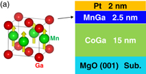
The films were fabricated by ultrahigh vacuum magnetron sputtering and the stacking structure was (001) MgO single-crystal substrate/CoGa (15)/MnGa (2.5)/Pt (2.0) (thickness is in nm). The film compositions of CoGa and MnGa were Co60Ga40 and Mn59Ga41, respectively, as estimated by inductively coupled plasma mass spectroscopy. X-ray diffraction measurements revealed that the B2-ordered paramagnetic CoGa buffer was epitaxially grown on the MgO substrate with (001) orientation. This CoGa buffer may promote the c-axis-oriented epitaxial growth of L10-ordered MnGa without significant interfacial reaction.30) The Cr/CoGa bilayer buffer is much better for the MnGa epitaxial growth,29,30) whereas it cannot be used in this study because Cr shunts the electrical current. The 2-nm-thick Pt layer was used here, which is the same as that used in a previous study of SOT in the Pt/Co/Al–O films.5) We also fabricated and characterized the films with the 5-nm-thick Pt capping layer. However, its PMA was highly deteriorated, indicating its unsuitability for this study.
Figure 1 shows a typical out-of-plane magnetization hysteresis loop for the film measured using a vibrating sample magnetometer. The saturation magnetization Ms of 150 ± 50 kA/m is smaller than that of a previously reported 3-nm-thick MnGa layer grown on a CoGa/Cr buffer and capped by a MgO barrier.30) This reduction in Ms may be mainly due to the atomic mixing of the MnGa and Pt capping layers and partially due to the slightly less ordering of the MnGa layer than that grown on the CoGa/Cr buffer layer. The surface roughnesses of CoGa and MnGa are also slightly larger than those reported previously. These structural properties may also lead to the non abrupt switching of magnetization at μ0Hc ≃ 110 mT, implying that magnetization reversal proceeds by pinning/depinning of the magnetic domain wall.
Download figure:
Standard image High-resolution image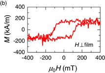
Fig. 1. (a) Illustration of the crystal structure of L10 MnGa and stacking structure of films. (b) Out-of-plane magnetization hysteresis loops of the film.
Download figure:
Standard image High-resolution imageThe film was then patterned into the micron sized Hall bar with Ti/Au electrodes by conventional ultraviolet photo-lithography and Ar ion milling. The Hall bars of six different sizes were formed on a substrate. Henceforth, we show the data for the smallest Hall bar. An optical microscopy image of the Hall bar is shown in Fig. 2(a). The length and width of the main Hall bar where the current I flows are 30 and 6 µm, respectively, and its resistance R was approximately 350 Ω. The resistance of the CoGa, MnGa, and Pt layers were evaluated for separately prepared samples, and the current flowing into the Pt layer I' is evaluated as I' = 0.44 × I. That is, approximately half of the total current flows into the thin Pt layer because of the very high resistivity of the CoGa and MnGa.31,32) The anomalous Hall resistance RH was measured at room temperature by measuring the voltage across the side Hall bars while injecting I. An out-of-plane magnetic field H or in-plane magnetic field HL parallel to the main Hall bar was applied, as shown in Fig. 2(a).

Fig. 2. (a) Image of the Hall devices and schematic of measurement geometry for out-of-plane magnetic field H and in-plane longitudinal magnetic field HL. Anomalous Hall resistance RH as a function of (b) H and (c) HL, which were measured at an electrical current I = 1 mA.
Download figure:
Standard image High-resolution imageFigure 2(b) shows RH–H curves. The hysteresis loops seen in the RH–H data is identical to the magnetization hysteresis loop [Fig. 1(b)] within the experimental errors, because of the proportionality of RH to the out-of-plane component of magnetization. RH was also measured as a function of HL using a physical properties measurement system [Fig. 2(c)]. The RH–HL data indicates a high PMA of the MnGa layer. For μ0HL > ±3 T, the RH value tends to be constant and close to zero. The direction of HL is not completely parallel to the film plane and there is a misalignment angle of approximately 1°, so that magnetization is slightly tilted from the in-plane direction, which is consistent with the non-zero and constant RH at high fields. The magnitude of RH increases gradually with decreasing magnitude of HL, corresponding to rotation of the magnetization. The effective PMA field  is evaluated to be
  T from the kink of the RH–HL data, indicating that the PMA thickness t product is
  mJ/m2.
According to a previous work,5) the current-induced magnetization switching measurement was performed while applying various HL. Typical RH–I data with μ0HL of −50, 0, and 50 mT are shown in Figs. 3(a)–3(c), respectively. The RH shows no clear magnetization hysteresis at μ0HL = 0 mT. However, the RH at μ0HL = ±50 mT exhibits a hysteresis loop similar to that in the RH–H data in Fig. 2(b), demonstrating current-induced magnetization switching. In the case of μ0HL = −50 mT, the magnetization switches from upward to downward at the switching current Ic ≃ −15 mA and switches from downward to upward at Ic ≃ 15 mA with sweeping I; that is, counter-clockwise hysteretic behavior is observed. On the other hand, clockwise hysteretic behavior is found for μ0HL = 50 mT, at which the magnetization switches at Ic with polarity opposite to those in Fig. 3(a). This change in the polarity of the switching current with different HL values is a unique feature in current-induced SOT magnetization switching.5) This unique feature may not be explained by the magnetic field generated from the current, the so-called Oersted's field, whose magnitude is estimated to be negligibly small, e.g., 3.1 mT at I = 15 mA.
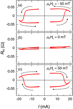
Fig. 3. Anomalous Hall resistance RH as a function of the electrical current I while applying the in-plane magnetic field (a) μ0HL = −50 mT, (b) 0 mT, and (c) 50 mT. Data points near I = 0 mA have been removed.
Download figure:
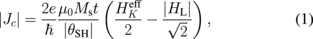
Standard image High-resolution imageWhen SOT originates from the spin-Hall effect (SHE), the switching current density Jc for films with perpendicular magnetization is expressed as33)
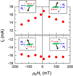
where e, ħ, and θSH are the electron charge, Dirac constant, and spin-Hall angle for a heavy metal layer, respectively. In this model, it is assumed that the magnetization uniformly rotates without thermal fluctuations at HL that is much smaller than  , and the current I flows only into the heavy metal layer. Figure 4 shows a phase diagram of the magnetization switching current Ic vs HL, which was evaluated from the RH–I data with different HL values. The absolute value of Ic systematically decreases with increasing magnitude of HL, which qualitatively agrees with Eq. (1), although the decrease in Ic for I < 0 is slower than that for I > 0.
Fig. 4. Phase diagram of the switching current Ic vs the in-plane magnetic field HL. Insets are illustration of the magnetization rotation for each set of Ic and HL.
Download figure:
Standard image High-resolution image
The current-induced magnetization switching from upward to downward (downward to upward) occurs when the direction of I is antiparallel (parallel) to HL in the MnGa/Pt film. This symmetry between I and HL is opposite to that in substrate/Pt/Co/Al–O films,5) in which the switching from upward to downward (downward to upward) occurred when the direction of I was parallel (antiparallel) to HL.5) This symmetry difference is reasonably accounted for by the fact that the direction of pure spin current generated from SHE is antisymmetric with respect to the current path above or below the magnetic layer. Thus, the symmetry in Fig. 4 is consistent with θSH > 0 for Pt.
Here, we note the result of similar experiments performed on using other samples prepared separately for reference. The similar SOT switching was reproduced in one sample with the same stacking structure. The SOT switching was also observed in the CoGa/MnGa (2 nm)/Pt (2 nm) structure, in which the thickness of MnGa was slightly smaller than that mentioned above. This thinner MnGa film exhibited a smaller Hc (∼50 mT), indicating that  decreases with decreasing thickness. Ic for this sample was lower than those shown in Figs. 3 and 4, e.g., Ic ≃ 10 mA at μ0HL = 50 mT. On the other hand, we observed no SOT switching in the CoGa/MnGa (2 nm)/Cu (5 nm) structure with the applied current used in this study. These features for different MnGa thicknesses and capping materials are also qualitatively in agreement with Eq. (1).
Finally, we briefly comment on the magnitude of Jc in this study. Equation (1) yields Jc = 1.2 × 10¹³ A/m2 at HL = 150 mT by substituting the experimental values of Ms,  , and t. Here, θSH = 0.11 for Pt was assumed,34) which may be the largest among the various reported values of θSH for Pt, ranging from ∼0.004 to ∼0.1.35) Thus, the above estimation of Jc is considered to be the lower bound for the theoretical Jc value. On the other hand, the experimental Jc, corresponding to the current density in the Pt layer at the switching, is ∼5.0 × 10¹¹ A/m2 at Ic = 13.5 mA and μ0HL = −150 mT, which is much smaller than that predicted from Eq. (1) and is comparable to the values reported for films with a lower PMA. There are many factors that reduce Jc in reality; e.g., the effects of a nonuniform magnetization process, the thermal fluctuation of magnetization, and the Joule heating effect.5,12–14) On the other hand, SOT is also considered to originate from the Rashba effect,3) whose existence has not yet been clarified in the present materials. In addition, it is likely that SOT due to the SHE in MnGa/Pt is significantly dependent on the nature of the interface because the antiferromagnetic MnPt shows a large θSH of up to 0.24.36) The clarification of these issues is obviously beyond the scope of this communication and will require future comprehensive studies.
In summary, current-induced magnetization switching was studied in Pt-capped 2.5-nm-thick MnGa films with PMA. A micron sized Hall bar device clearly showed magnetization switching as a function of in-plane electrical current, depending on the direction of the longitudinal in-plane magnetic field. The switching phase diagram qualitatively agreed with that of SOT due to the SHE for the Pt layer. This study demonstrated that SOT switching was possible in Mn-based magnets with a large PMA with moderate electrical current density.
Acknowledgments
This work is partially supported by a Grant-in-Aid for Scientific Research (No. 16H03846), the ImPACT Program, and the Asahi Glass Foundation. Y.S. acknowledges the GP Spin program. The authors thank Y. Kondo for technical assistance and T. Miyazaki for valuable comments.