
Abstract
We developed the epitaxial growth technique of various kinds of nanodots (NDs) on Si substrates using ultrathin SiO2 film. Fe-based NDs were epitaxially grown on Si substrates without intermixing with Si atoms in Si substrates despite the easy reaction of Si and Fe, resulting in atomically sharp interfaces between NDs and substrates. The status control of the nuclei was important at the nucleation stage in terms of control of ND crystal structure. The proper nuclei also suppressed the undesirable reactions such as intermixing of Fe and Si in Si substrates. The epitaxial NDs formed by our technique can supply the prospect for the application to some devices.
Export citation and abstract BibTeX RIS
1. Introduction
Nanodots (NDs) have been intensively studied because of their various applications such as optoelectronic devices, magnetic devices,1–5) and so on. A main advantage of NDs is that quantum confinement effects and low dimensional properties6) can bring the new or high efficiency devices. For example, in the optical device field, epitaxial Si or Ge NDs on Si substrates have been studied for the realization of light emitter for Si photonics.7–9)
From a material viewpoint, in addition to Si or Ge which are widely used for LSI, Fe-based materials have drawn much attention because of the eco-friendly and abundant elements. One of the interesting materials is β-FeSi2 because of its prospect for light emitting diode.10–16) Other Fe-based materials have also attracted much interest due to other possible applications such as spintronic or magnetic devices using the magnetic properties in iron, its oxide,17–19) its silicide20–22) and germanide, and resistance random access memory using resistive switching properties in iron oxide. Recently, skyrmions were observed in ε-FeGe(Si),23–25) leading to a large interest in Fe-based materials.
One of the barriers to realize Fe-based devices is the difficulty in formation of high quality and high purity single crystals on Si substrates. In terms of the ND formation, it is difficult to grow epitaxially on Si substrates with atomically sharp interfaces because of the easy reaction between Fe and Si. We developed epitaxial growth technique of NDs of various kinds of materials such as Si, Ge, GeSn, GaSb, and iron silicide on Si substrates using ultrathin SiO2 films.26–32) The NDs were epitaxially grown on Si substrates through the nanowindows in the ultrathin SiO2 films and had sharp interfaces. The NDs also have no misfit dislocations owing to elastic strain relaxation.33,34) Here, we introduce this growth technique and modify it to form the iron oxide and iron germanide NDs with ultrahigh density.35,36) In this growth technique, the status control of the nuclei is important at the nucleation stage. The status of the nuclei on substrates determines the crystal structure of NDs. The proper choice of nucleus material suppresses the undesirable reactions such as intermixing of Fe and Si in Si substrates. The epitaxial NDs formed by our technique can supply the prospect for the application to some devices.
2. Experimental methods
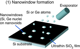
Chemically-cleaned Si wafers were introduced into the molecular beam epitaxy (MBE) chamber equipped with reflection high energy electron diffraction (RHEED) at the base pressure of ∼1 × 10⁻⁸ Pa. Clean Si surfaces were prepared by formation of 100-nm-thick buffer layers at 500 °C on Si substrates. In other cases, samples cut from Si wafers were introduced into MBE chamber. Clean Si surfaces were obtained by flashing at 1250 °C after degassing at 500 °C. The samples were oxidized at 400–600 °C for 10 min at oxygen pressure of 10−4–10−5 Pa to form ultrathin SiO2 films. The thickness of ultrathin SiO2 films was ∼1 monolayer (ML). First, for nucleus formation, Ge or Si was deposited onto the ultrathin SiO2 films at 500–630 °C. During this process, ultrahigh density nanometer-sized voids (nanovoids) were formed in the ultrathin SiO2 films through the reaction: SiO2 + Ge → SiO↑ + GeO↑ or SiO2 + Si → 2SiO↑, and then subsequently deposited Ge or Si atoms were trapped at these nanovoids to form a high density of epitaxial nuclei.26–36) The epitaxial nuclei on nanovoids were referred to as nanowinodows. Then, materials of NDs were deposited onto the ultrathin SiO2 films with epitaxial nuclei at various temperatures to form a high density NDs. These NDs were contacted with Si substrates through nanowindows in the ultrathin SiO2 films resulting in the epitaxial growth.
RHEED patterns were obtained using electron beam along 〈112〉 for Si(111) substrates and 〈110〉 for Si(001) substrates. Scanning tunneling microscope (STM) images were acquired at room temperature (RT) with atomically sharp W tips.37)
3. Si or Ge nanodots epitaxially grown on Si substrates by ultrathin SiO2 film technique
3.1. Formation of Si or Ge nanodots
One ML of Si surfaces was oxidized under the condition: O2 pressure of 10−5–10−4 Pa at 400–600 °C to form the ultrathin SiO2 films. The films have amorphous morphology confirmed by STM and RHEED. Si or Ge atoms were deposited on the ultrathin SiO2 films to form Si or Ge NDs. STM images of the Si and Ge NDs are shown in Figs. 1(a) and 1(b), where 8 ML Si and 5 ML Ge were deposited at 500 °C respectively. 5 nm spherical NDs seemed to be formed on Si substrates with an ultrahigh density of ∼2 × 1012 cm−2. RHEED patterns indicated that at deposition temperature higher than ∼450 °C, NDs were epitaxially grown on Si substrates, while at deposition temperature lower than ∼400 °C, RHEED of NDs exhibited Debye ring pattern revealing non-epitaxial growth of NDs.

Fig. 1. STM images of Si (a) and Ge NDs [(b) and (c)] on Si(111) substrates formed by deposition of 8 ML Si (a) and 5 ML Ge (b) on the ultrathin SiO2 films, or by deposition on 4.4 ML Ge (c) on the ultrathin SiGe oxide films.
Download figure:
Standard image High-resolution imageFormation mechanism was reported everywhere as follows.26,27,38) At the first stage of Si or Ge deposition on the ultrathin SiO2 films, deposited atoms diffuse on the surfaces until they react with the ultrathin SiO2 films through the following reactions:

As a result, the nanovoids are formed in the ultrathin SiO2 films. The distance between nanovoids is determined by diffusion length of deposited atoms until they react with the ultrathin SiO2 films. In the case of Si and Ge, this value is approximately 10 nm resulting in the ultrahigh density (∼1012 cm−2). Extra Si or Ge atoms are trapped at the nanovoids because nanovoids with dangling bonds are energetically stable sites for deposited atoms compared with the ultrathin SiO2 film sites. In other words, the chemical potential of deposited atoms at the nanovoid sites is smaller than that on the ultrathin SiO2 film. As a result, ultrasmall Si or Ge nuclei on nanovoids are formed, which are called as nanowindows. Then, nanowindows work as nucleation sites for ND growth by subsequent deposition resulting in the formation of ultrahigh density spherical NDs. When the deposition temperature is high ( 450 °C), nanowindows form sufficiently through reaction (1). As a result, the formed NDs contact with Si substrates through nanowindows leading to the epitaxial growth. On the contrary, when the deposition temperature is low (
 400 °C), nanowindows do not penetrated into Si substrates due to insufficiency of reaction (1), resulting in non-epitaxial growth of NDs. As for epitaxial NDs, the limited nanocontact between NDs and substrates reduces the strain energy in NDs induced by lattice mismatch. The NDs are elastically-strain relaxed and have no misfit dislocation due to the small strain energy and spherical shape. This technique for ND growth can be applied to the ultrathin SiGeOx films,39) as shown in Fig. 1(c).
3.2. Modification of the technique for other material NDs
We paid attention to the ultrathin SiO2 film with Si or Ge nanowindows as a template for ND growth, and modified the aforementioned ultrathin SiO2 film technique. As shown in Fig. 2, first, we predeposited a small amount of Si of Ge on the ultrathin SiO2 film to form ultrahigh density nanowindows. Second, atoms A and B were deposited simultaneously on the ultrathin SiO2 film with nanowiondws with flux ratio of 1 − x to x to form epitaxial A1−xBx NDs. Thus, the modified technique for ND growth can be applied to various materials. In this technique, we expected that the atoms A and B are trapped at the nanowidow sites, and then, ultrahigh density NDs were formed. Furthermore, NDs were epitaxailly grown on Si substrates by nancontact between NDs and substrates through nanowindows. In this case, as is the case with Si or Ge, limited contact between NDs and Si substrates enables elastic strain-relaxation in spherical NDs without introduction of misfit dislocations at their heterointerfaces.32–34) In Fig. 3, STM images of the various kinds of NDs are shown.30,31,40) The NDs are epitaxially grown on Si substrates, which were confirmed by RHEED patterns.
Download figure:
Standard image High-resolution image
Fig. 2. Schematic of the modified ultrathin SiO2 film technique.
Download figure:
Standard image High-resolution image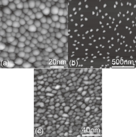
Fig. 3. STM images of 8 ML GeSn NDs (a), 8 ML GaSb NDs (b), and 12 ML β-FeSi2 NDs epitaxailly grown on Si substrates using ultrathin SiO2 films.
Download figure:
Standard image High-resolution imageIn the case of β-FeSi2 NDs on Si(001) substrates, the formation process is a little different from those on Si(111) substrates. 2 ML Si was deposited on the ultrathin SiO2 films at 670 °C to form nanowindows. Fe and Si were codeposited on the ultrathin SiO2 film at RT to form ultrahigh density amorphous iron silicide NDs. Then, the NDs were crystalized to epitaxial β-FeSi2 ones by annealing at 450–650 °C. This technique is a solid phase epitaxy on the ultrathin SiO2 films. ND shape and size strongly depended on the annealing temperatures.
The NDs exhibited the quantum confinement effects. The energy bandgaps of individual Ge and GeSn NDs were measured by scanning tunneling spectroscopy, which depended on ND size. The dependences are explained by the quantum confinement effect.
It was confirmed that the β-FeSi2 NDs on Si(111) and (001) surfaces were indirect-transition semiconductor using STM-EFMS that is photoabsorption spectroscopy measurement with nanometer-sized special resolution41) by comparing with bulk and film results.42,43)
4. Application of the iron silicide nanodots to light emitting material
We formed β-FeSi2 NDs epitaxially grown on Si(111) and (001) substrates as mentioned in the previous section. The RHEED patterns demonstrated that NDs are epitaxially-grown β-FeSi2 which configurations are (110)β-FeSi2/(111)Si or (101)β-FeSi2/(111)Si for Si(111) substrates and (100)β-FeSi2/(001)Si for Si(001) substrates.44) The morphology of the NDs was changed by annealing process. The ND shape was kept to be domed during low temperature annealing (<550 °C), while NDs changed to the flat, square ones by the higher annealing temperature (>600 °C) (Fig. 4). The ultrahigh density (∼1012 cm−2) in domed NDs was decreased to ∼1011 cm−2 in flat NDs due to the coalescence by high temperature annealing.
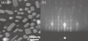
Fig. 4. STM image (a) and RHEED pattern (b) of 15-ML β-FeSi2 flat NDs epitaxially grown on Si(111) substrates.
Download figure:
Standard image High-resolution imageTo measure the light emitting property of the samples, Si cap layers were formed by Si deposition on the β-FeSi2 NDs/Si at 450–550 °C. RHEED pattern demonstrated the Si cap layers grew epitaxially with the same crystal orientations as the Si substrates. To measure the PL spectra of Si/β-FeSi2 NDs/Si structures, we formed 12 ML flat β-FeSi2 NDs using ultrathin SiO2 film technique, annealed the NDs in vacuum at 650 °C, and fabricated Si cap layer on them. The PL spectra are shown in Fig. 5. For crystallinity enhancement, the samples were post-annealed at 800 °C for 30 min in N2 for Si(111) case and at 900 °C for 10 s for Si(001) case. Broad PL peak around ∼0.83–0.86 eV was observed in both samples.45) For the Si(111) substrates, the Si peak related to TO phonons and sharp D1–D4 lines appear, in addition to a strong, broad peak around 0.83–86 eV. This broad peak is similar to that in the case of Si(001) substrates. Closer look at PL spectra indicated the multiple peaks at 0.90, 0.93, and 1.0 eV also appeared in the Si(001) case, but it is difficult to deconvolve them unlike the Si(111) case.

Fig. 5. PL spectra of Si-capped 12-ML β-FeSi2 flat NDs epitaxially grown on Si(111) and (001) substrates at ∼4 K.
Download figure:
Standard image High-resolution imageWe measured the temperature dependence of the PL spectra for the above post-annealed Si/β-FeSi2 NDs/Si structures. In the case of β-FeSi2 ND/Si(111), it was confirmed that D lines (D2, D3, and D4) rapidly disappeared with increasing measurement temperature (>50 K), which is as reported in some papers.46,47) In β-FeSi2 ND/Si(001), the multiple peaks at ∼0.90, 0.93, and 1.0 eV also disappeared by increasing measurement temperature (>50 K). These results indicate that these rapidly-extinguished multiple peaks in the case of Si(001) could be related to D lines. On the other hand, broad PL peak (0.83–0.86 eV) continued to be observed in the temperature range lower than 200 K in both substrate cases although the intensity of this broad PL peak decreased with measurement temperature.45) These features were independent of the crystal orientation of the Si substrate. This broad peak is similar to the Si layer cases on the ultrathin SiO2 films.48)
We focused on the broad PL peak (0.83–0.86 eV) and measured electroluminescence (EL) of Si/flat β-FeSi2 NDs/Si(001) structures which were post-annealed at 900 °C for 10 s. EL was observed at 4 K with a current threshold of ∼15 mA.45) Electric field during EL measurement occurred in "non-doped" Si cap layer connected with n-type Si substrates. Because the Si cap layers were not doped, electron–hole pairs could also be generated in the Si cap layer regions by energetic relaxation of hot electrons injected from the electrode — essentially, impact ionization — not by conventional electron injection.49,50) Because the structure presented here was not optimized for EL, we expect that the luminescence intensity can be further enhanced by improving the structure.
5. Other Fe-based nanodot formation
5.1. Fe oxide nanodots on Si substrates for ReRAM
The rapid progress of information technology has largely relied on the development of nonvolatile memories. Recently, ReRAM has attracted much attention as one of the promising next generation nonvolatile memories.51–55) It has advantages such as low power consumption, high switching speed. Operation of ReRAM is based on a resistive switching effect in various metal oxides. Fe oxide, composed of abundant and earth-friendly elements, shows a resistive switching effect.56–58) We focused on Fe oxide grown on Si substrates because of their industrial advantages such as low cost, nontoxicity, and compatibility with existing Si process technology. Resistive switching in Fe oxide is reportedly caused by crystal structure changes between high resistance γ-Fe2O3 and low resistance Fe3O4 due to the oxygen vacancy movement. Compared with other materials with resistive switching effect, the resistance ratio between high and low resistance states, (OFF/ON ratio), was very poor (∼10).57) One of the causes can be the existence of crystal defects inducing the leakage current in low quality Fe oxide. Therefore, it is needed to form high quality Fe oxide epitaxially grown on Si substrates. We focused on single crystalline Fe oxide NDs epitaxially grown on Si substrates, where in a ND, there are no crystal boundaries and less crystal defects caused by crystal lattice mismatch.
There are many methods to form Fe oxide NDs, but in terms of epitaxial growth on Si substrates, there are not so many fabrication methods. One method can be the oxidation of the Fe NDs epitaxially grown on Si substrates. In addition to Fe oxide NDs for ReRAM, magnetic nanoparticles such as Fe and its oxide NDs have the potential to be applied as high-density magnetic storage media. Therefore, epitaxial growth of Fe and Fe oxide NDs on Si substrates is very meaningful for information technology. One of the difficulties in the epitaxial growth of Fe-based films/NDs on Si substrates is unintentional silicidation introducing the defective interfaces. For epitaxial growth, it is needed to use of buffer layers of insulators such as MgO or TiN59–62) which are not suitable for ReRAM with flowing electric current. Up to now, there are no methods of direct epitaxial growth on Si substrates avoiding the silicidation.
The ultrathin SiO2 film technique for epitaxial growth of iron silicide NDs on Si substrates has been developed where the interdiffusion between deposited Fe atoms and Si atoms in substrates was suppressed.40) However, Fe ND formation using ultrathin SiO2 film technique has been not investigated minutely. Here, we present the formation technique of Fe-based NDs using ultrathin SiO2 film technique.
5.2. Epitaxial growth without silicidation by interface control
We tried to develop the epitaxial growth technique of Fe NDs using the ultrathin SiO2 films with Si nanowindows. 1 ML Si was deposited on the ultrathin SiO2 films on Si(111) substrates at 600 °C to form the Si nanowindows. Fe (12–36 ML) was deposited on the ultrathin SiO2 films with Si nanowindows at ∼100–350 °C. The STM images in Fig. 6 show the NDs grown under the various Fe deposition conditions in the case of the nanowindow formation in the ultrathin SiO2 films at 600 °C. The average ND diameter and the density of formed NDs were summarized in Figs. 6(g) and 6(h). The ND diameter was ranging from 3 to 7 nm, and ND diameter became larger with increase of Fe deposition amount. The ND density is ultrahigh [(2–5) × 1012 cm−2].
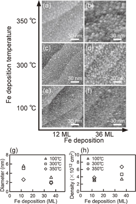
Fig. 6. (a)–(f) STM images of NDs formed by 12–36 ML Fe deposition at ∼100–350 °C on the ultrathin SO2 films with nanowindows formed by Si predeposition at 600 °C on Si(111) substrates. Average diameter (g) and density (h) of NDs. Fe deposition temperature was denoted in the graphs.
Download figure:
Standard image High-resolution imageFigures 7(a)–7(f) show the RHEED patterns of the NDs on Si(111) substrates grown under various Fe deposition conditions in this nanowindow formation case (Si deposition at 600 °C). Electron incident direction in RHEED observation was 〈112〉Si. In the case of NDs formed by deposition of 12 ML Fe at ∼100 °C, RHEED pattern was too obscure due to the poor crystallinity and the small volume, while in the case of other NDs, diffraction spots were observed indicating that ultrahigh density NDs shown in Figs. 6(a)–6(f) were epitaxially grown on Si substrates. Closer investigation of RHEED patterns enabled the clarification of the crystal structure of formed NDs. For ε-FeSi NDs epitaxailly grown on Si substrates with ε-FeSi(111)/Si(111), the diffraction spots are appeared at the 1/3 position of the 1 × 1 Si diffraction streaks in RHEED patterns. The RHEED patterns of Fe3Si, c-FeSi, and Fe NDs, which are similar to each other, are shown in Fig. 7(g). If NDs are composed of pure Fe ones epitaxially grown with Fe(111)/Si(111) without iron silicides, the pattern of bcc Fe shown in schematic in Fig. 7(g) appears, where the 111 for c-FeSi or 222 for Fe3Si spot pointed by an arrow are not observed. For the NDs formed by Fe deposition at 350 °C, the 1/3 spots pointed by arrows were appeared in RHEED pattern, which indicated that these NDs included ε-FeSi. In the case of at lower Fe deposition temperature (100–300 °C), 1/3 spots did not appear, but it is not clear whether the silicide spots (111 for c-FeSi or 222 for Fe3Si) existed which are shown by an arrow in Fig. 7(g). Therefore, we investigated the line profiles between points A and B in RHEED patterns in Figs. 7(c), 7(d), and 7(f). The line profiles are show in Fig. 7(h). The peaks were observed as pointed out by dotted circles in Fig. 7(h), which corresponded to 111 for c-FeSi or 222 for Fe3Si indicating the existence of Fe silicide. By this means, in the case of nanowindow formation by Si deposition at 600 °C, the formation diagram was acquired as shown in Fig. 8. The epitaxial NDs were not composed of pure Fe, but included Fe silicide. This result indicated that in the case of nanowindow formation by Si deposition at 600 °C, the interdiffusion of Fe and Si in substrates took place. It was considered that interdifussion occurred through the nanowindows in ultrathin SiO2 films at ∼100 °C not directly beyond the ultrathin SiO2 films according to the report that Fe atoms were not able to diffuse beyond the ultrathin SiO2 films to Si substrates at low temperature.63)
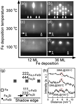
Fig. 7. (a)–(f) RHEED patterns of NDs formed by 12–36 ML Fe deposition at ∼100–350 °C on the ultrathin SiO2 films with nanowindows formed by Si predeposition at 600 °C on Si(111) substrates. (g) RHEED patterns of Fe3Si, c-FeSi, and Fe NDs. (h) Line profiles on between points A and B indicated by the arrows.
Download figure:
Standard image High-resolution image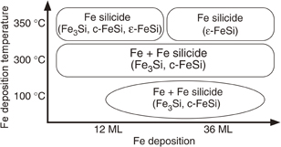
Fig. 8. Formation diagram of the NDs formed by Fe deposition on the ultrathin SiO2 films with nanowindows formed by Si predeposition at 600 °C.
Download figure:
Standard image High-resolution imageTo prevent the interdiffusion of Fe and Si, we tried to reduce the nanowindow size by decreasing Si deposition temperature for forming nanowindows in the ultrathin SiO2 films. Nanowindows were formed through the reaction shown by Eq. (1). Therefore, at lower Si deposition temperature, the reaction speed is reduced, resulting in smaller nanowindows. We formed nanowindows in the ultrathin SiO2 films by 1 ML Si deposition at low temperature of 450 °C, and then deposited Fe deposition (12–36 ML) at ∼100 °C to form NDs. Figures 9(a)–9(c) show the RHEED patterns of the NDs indicating the diffraction pattern of epitaxially grown bcc-Fe. To clarify whether Fe silicide is included, we investigated the line profile between points A and B in RHEED [Fig. 9(c)], which is shown in Fig. 9(d). There is no peak corresponding to 111 spot for FeSi or 222 spot for Fe3Si. This result indicates that the formed NDs were composed of Fe within the RHEED observation. Figures 9(e)–9(g) show the RHEED patterns of the NDs in the case of nanowindow formation temperature of 400 °C. Debye rings appeared indicating non-epitaxial NDs.
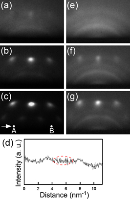
Fig. 9. (a)–(c) RHEED patterns of the NDs formed by 12 (a), 24 (b), and 36 (c) ML Fe deposition at ∼100 °C on the ultrathin SiO2 film with the nanowindows formed by Si predeposition at 450 °C. (d) Line profile between points A and B indicated by the arrow. (e)–(g) RHEED patterns of the NDs formed by 12 (e), 24 (f), and 36 (g) ML Fe deposition at ∼100 °C on the ultrathin SiO2 film with the nanowindows formed by Si predeposition at 400 °C.
Download figure:
Standard image High-resolution imageAs mentioned above, we aimed at changing nanowindow size by tuning Si deposition temperature for nanowindow formation. As a result, the strong dependence of ND growth on the Si deposition temperature was found. In the case of high nanowindow formation temperature (600 °C), Fe silicide such as Fe3Si and c-FeSi were formed even when the Fe was deposited at low temperature (∼100 °C). In this case, the nanowindows were expected to be large to cause the interdiffusion of Fe and Si through them, as shown in Fig. 10. To make the nanowindows smaller, we reduced the nanowindow formation temperatures from 600 to 450 °C. In this case, the silicide were not observed indicating that the interdiffusion did not occur through nanowindows. As a result, pure Fe NDs were epitaxially grown on Si substrates. The epitaxial growth means that NDs contacted with Si substrates through nanowindows. On the other hand, at lower nanowindow formation temperature of 400 °C, the non-epitaxial NDs were formed. This is because nanowindow formation through reaction (1) did not proceed sufficiently at the lower temperature. As a result, the contact between NDs and Si substrates was not enough leading to non-epitaxial growth. The appropriate size of nanowindow is necessary for pure Fe NDs to grow epitaxially on Si substrates. In this case, the nanowindows formed by Si deposition at 450 °C were expected to have the most appropriate condition.
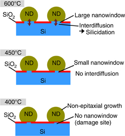
Fig. 10. Illustration of the dependence of NDs on temperature at Si predeposition.
Download figure:
Standard image High-resolution image5.3. Oxidation without silicidation by interface control
36 ML Fe NDs were epitaxially grown on Si substrates using the ultrathin SiO2 films with nanowindows formed by 1 ML Si deposition at 450 °C. The NDs were exposed to O2 at 1 atm and RT. From STM image of the oxygen-exposed NDs, the ND density was found to be maintained at 2 × 1012 cm−2, while RHEED patterns showed changes from bcc crystal to an amorphous structure after exposure to oxygen. To estimate O2 composition in the oxygen-exposed NDs, ex-situ X-ray photoelectron spectroscopy (XPS) were measured, revealing that oxygen-exposed NDs were oxidized at RT to be Fe2O3 NDs. XPS also revealed the existence of SiO2.
Figure 11(a) shows cross sectional transmission electron microscope (HRTEM) image of the oxygen-exposed Fe NDs. HRTEM images showed the existence of amorphous NDs as indicated by the dotted circles in Fig. 11(a). The results of XPS and RHEED suggested these NDs were amorphous Fe2O3. In the layer beneath the Fe2O3 NDs, a second amorphous layer was observed to be SiO2. The layer below the SiO2 films was observed to be composed of crystalline and amorphous regions. FFT analysis of HRTEM images revealed that the crystal layer was Fe3Si epitaxially grown on the Si substrates. The amorphous layer below the crystalline Fe3Si appeared to be amorphous Fe silicide (a-silicide) resulting from incomplete silicidation.35)
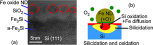
Fig. 11. (a) Cross sectional HRTEM image of oxygen-exposed Fe NDs. (b) Schematic of reaction between epitaxial Fe NDs and Si substrates during oxygen exposure.
Download figure:
Standard image High-resolution imageWhen ultrathin SiO2 films without Fe NDs are exposed to the atmosphere at room temperature, ultrathin SiO2 films protects the further oxidation of Si substrates.64,65) Additionally, before oxygen exposure, Fe deposition at ∼100 °C did not lead to silicidation on the ultrathin SiO2 films with Si nanowindows formed at 450 °C as mentioned in the previous section. This indicated that oxygen exposure of the Fe NDs caused the Si oxidation and alloying of the Si and Fe at room temperature, as shown in Fig. 11(b). At the first stage of oxygen exposure, oxygen atoms were considered to go into Fe NDs and Si can be oxidized slightly near the interface with Si substrates. In the case of Fe films on Si that include a small proportion of oxygen (<2%),66) there is a report that Fe atoms were able to diffuse into Si substrates owing to the presence of small amounts of oxygen atoms. If this mechanism66) can be applied to our case, Fe atoms in Fe NDs including oxygen atoms diffuse into Si substrates resulting in the silicidation. In this framework, the aforementioned Fe diffusion accompanied by SiO2 formation and silicidation should occur predominantly through nanowindows just below NDs, where NDs and Si were directly contacted. Furthermore, the existence of the a-silicide layer below the crystalline silicide layer can be reasonably explained by this mechanism, considering this amorphous layer as the reaction surface of silicidation.
To prove this mechanism, we tried to prevent Fe diffusion into Si in the presence of oxygen. We used Ge nanowindows, namely Ge nulcei on nanovoids, in the ultrathin SiO2 films instead of Si nanowindows by depositing 5 ML Ge onto the ultrathin SiO2 film at 620 °C. Fe was deposited on the ultrathin SiO2 films with Ge nanowindows at 100 °C. STM and RHEED observations demonstrated that bcc-Fe NDs of several nanometer in diameter were epitaxial grown on Si substrates. The bcc-Fe NDs were exposed to oxygen at 1 atm, and then, the NDs of ∼10 nm in diameter were observed. A HRTEM image of oxygen-exposed Fe NDs displayed that flattened Fe oxide NDs were formed on epitaxial Ge nuclei on Si substrates. In the area of that Ge nuclei existed, there was no SiO2 layer and no silicidation layer below the Ge nuclei. In areas without Ge nuclei, the 2-nm-thick SiO2 above flat layers of 1 nm silicide were observed, but the thicknesses of silicide layer was smaller than the Si nanowindows case. This indicated that when Ge nuclei were present between the Fe NDs and Si substrates, oxygen-assisted Fe diffusion into Si did not occur, and silicidation and SiO2 formation were suppressed.35)
This demonstrated that the nanometer-sized interface between NDs and the substrates had remarkable influence on the interfacial reaction between Fe NDs and the substrate. Furthermore, control over the nanometer-sized interface is important for the use of Fe-based NDs on substrates with sharp interfaces, which could be an important general principle in system of NDs on substrates.
5.4. Crystal structure control by nucleation control
As mentioned in the previous section, Ge nanowindows work as barrier for silicidation between Fe and Si in substrates. In addition to the interest in the aforementioned Fe/Ge system, iron germanide has drawn much attention. Recent reports have invoked observations of Skyrmions in ε-FeGe(Si), that is a cubic B20 structure with chirality.23–25) Another crystal structure of iron germanide, Fe1.7Ge with a hexagonal B82 structure, has also been studied as a ferromagnetic material.67) In addition to the films, nanostructures of iron germanide on Si substrates are of great interest because nanostructuring can yield new properties and new physics. However, epitaxial growth of Fe(Ge)/Si with sharp interfaces is difficult because the interfaces are easily disordered due to silicidation (germanidation),68–71) leading to non-controllable electronic states and a dead layer at the interface. Furthermore, the crystal structure control in this system is difficult owing to the complicated phase diagram. Therefore, a nanostructure formation technique with a well-controlled interface and crystal structure is crucially needed for this system.
We have developed an epitaxial growth technique for Fe NDs on small Ge nuclei35) by applying an ultrathin SiO2 film technique. Now, we focus on use of these Ge nuclei as germanidation sites for epitaxial growth of iron gemanide NDs on Si substrates with sharp interfaces. We find that the crystal structure can be selected by controlling status of Ge nuclei.
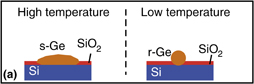
We formed two kinds of Ge nanowiondws (Ge nuclei on nanovoids) in the ultrathin SiO2 films by Ge deposition on the ultrathin SiO2 films at 500 and 630 °C. Ge deposition at higher temperature get nanovoid size larger. Fattened Ge nuclei on large nanovoids were formed at Ge deposition temperature of 630 °C because of the larger naowindows at high deposition temperature, while at the Ge deposition temperature less than 600 °C, spherical Ge nuclei were formed. It was confirmed by RHEED and TEM that the flattened Ge nuclei were strained (s-Ge) due to the large contact area with substrates, while spherical Ge nuclei were elastically-strain-relaxed without misfit dislocation (r-Ge) owing to the small contact and its spherical shape. The lattice constant of s-Ge (r-Ge) is close to bulk Si (Ge), which is confirmed by RHEED pattern. This is illustrated in Fig. 12(a). To form iron germanide NDs, we deposited 5 and 7 ML Fe on the two kinds of Ge nuclei (s- or r-Ge nuclei) at ∼280 °C, which is a relatively high temperature compared with Fe ND case (∼100 °C). STM images demonstrate that the formed Fe-based NDs were flattened and spherical in the case of the s- and r-Ge nuclei, respectively. The ND density was the same as that of the Ge nuclei in both cases indicating that the Ge nuclei act as nucleation sites for Fe-based ND formation. The RHEED patterns implied that Fe1.7Ge with the B82 structure67) was epitaxially grown on the Si substrates for r-Ge NDs, while ε-FeGe with the B20 structure was epitaxially grown on the Si substrates for s-Ge NDs. Fe1.7Ge with the hexagonal phase is thermodynamically stable for a narrow stoichiometry interval ranging approximately from Fe2Ge to Fe1.5Ge. This is illustrated in Fig. 12(b). This can be explained by considering that the elastic strain energy largely contributed to free energy variation between various crystal structures of Fe-based NDs because the lattice mismatches in epitaxial growth on Si(111) between ε-FeGe and Si and between Fe1.7Ge and Ge are both almost zero. This means that the crystal structure of iron germanide is determined by the elastic strain energy during the first stage of epitaxial growth, namely nucleation. As a result, by controlling the strain state, the lattice constant of the Ge nuclei working nucleation sites, the crystal structure of the epitaxially grown iron germanide could be selected.
Download figure:
Standard image High-resolution image
Fig. 12. (a) Cross-sectional schematics of flattened s-Ge NDs and spherical r-Ge NDs formed at 630 °C and low temperature (<600 °C), respectively. (b) Cross-sectional schematics of ε-FeGe and Fe1.7Ge NDs formed by Fe deposition on s-Ge NDs and r-Fe NDs, respectively.
Download figure:
Standard image High-resolution image
6. Conclusions
The ultrathin SiO2 film technique for epitaxial growth of various materials of NDs was presented. By modifying it, Fe-based NDs were epitaxially grown on Si substrates with sharp interfaces. To obtain Fe oxide NDs with sharp interfaces, Fe NDs on Ge nanowindows were oxidized. Nanometer-sized interface of Ge nuclei suppressed undesirable reaction such as silicidation, and Si oxidiation. Also, strain status of Ge nuclei determined the crystal structure of Fe germanide NDs. These results demonstrated that the material and strain status of the nuclei for the ND growth are key to formation of Fe-based NDs on Si substrates.
Acknowledgments
This work was supported in part by a JST-PRESTO program (Y. Nakamura). It was also supported by a Grant-in-Aid for Scientific Research B (25286026) and a Grant-in-Aid for Exploratory Research (25600016). Also, this work was partially supported by TEPCO Memorial Foundation, Research Grant (Basic research).