
Abstract
We grew epitaxial layers on 4H-SiC C-face substrates with a 1° off-angle, and discussed important factors related to stacking fault (SF) density reduction by investigating the causes of SFs. Three types of SFs were generated, namely 3C inclusions, 8H-SFs and  -SFs. The 3C inclusions were caused by 3C-SiC particles, which were present on the substrates before epitaxial growth, or which had fallen onto the substrates during epitaxial growth from the inside walls of a chemical vapor deposition reactor. The 3C-inclusion density decreased when the in-situ H2 etching depth exceeded 0.4 µm because the 3C-SiC particles, which were present on substrates before epitaxial growth, were removed. For 8H-SFs and
  -SFs, high dislocation density areas on the substrates rather than the dislocations themselves cause these SFs. To reduce the density of these SFs, it is important to suppress generation of the high dislocation density areas on the substrates.
Export citation and abstract BibTeX RIS
1. Introduction
Silicon carbide (SiC) is expected to be widely used for power devices because the power conversion efficiency of SiC devices is higher than that of silicon devices. Of the many polytypes such as 4H, 6H, and 3C, 4H-SiC is mainly used for developing SiC power devices because of certain physical properties such as its wider bandgap and higher electron mobility.
The homoepitaxial growth of 4H-SiC layers is necessary in order to control the doping concentration and thus produce functional 4H-SiC devices. This is because SiC boules are usually grown by sublimation but it is difficult to control the doping concentration using this technique. 4H-SiC homoepitaxial growth without other-polytype inclusions has been achieved by using substrates with several off-angles1,2) although other-polytype inclusions are easily generated because of their low formation energy.3,4) Now, substrates with a 4° off-angle are employed commercially. To take account of polarity, Si-face substrates are mainly used because they result in less residual nitrogen incorporation than C-face substrates.2) Therefore, 4H-SiC Si-face epitaxial growth on substrates with a 4° off-angle is the standard technique for fabricating SiC devices.
However, it is important that we reduce the off-angle and use C-face substrates if we are to improve the properties of SiC trench metal–oxide–semiconductor field-effect transistors (MOSFETs). Trench MOSFETs are well known to have low on-resistances due to their high cell density, but there are two serious challenges that must be overcome before we can improve the properties. One challenge is to find way to suppress the anisotropic channel properties on the trench sidewalls such as the channel mobility and threshold voltage.5) The anisotropic channel properties are caused by large off-angles such as 8 and 4° when the trench sidewalls are not parallel to the step flow direction, i.e., the ![$[11\bar{2}0]$](https://content.cld.iop.org/journals/1347-4065/54/4S/04DP04/revision1/SS14078if003.gif) direction.5) It has been reported that reducing the off-angle is effective for suppressing the anisotropic properties.5) The other challenge is to improve reliability, which is reportedly enhanced by using C-face substrates.6) Therefore, 4H-SiC homoepitaxial growth on C-face substrates with an off-angle of less than 4° is a possible way of improving the trench MOSFET properties.
direction.5) It has been reported that reducing the off-angle is effective for suppressing the anisotropic properties.5) The other challenge is to improve reliability, which is reportedly enhanced by using C-face substrates.6) Therefore, 4H-SiC homoepitaxial growth on C-face substrates with an off-angle of less than 4° is a possible way of improving the trench MOSFET properties.
For device applications of C-face epitaxial layers with a lower off-angle, it is extremely important to reduce the decrease of background carrier concentration and stacking fault (SF) density. For example, a background carrier concentration of the order of 1014 cm−3 is required for 3.3 kV MOSFETs because the required drift layer carrier concentration is around 3 × 1015 cm−3. The background carrier concentration should be reduced to about 1014 cm−3 for high-voltage devices. The background carrier concentration of C-face epitaxial layers can be reduced to around 1014 cm−3 by increasing the C/Si ratio due to a site competition effect even though the residual nitrogen incorporation of C-face epitaxial layers is more intense than that of Si-face epitaxial layers.7–9) The area of SFs increases as the off-angle decreases. This means that the usable area of epitaxial layers with a lower off-angle is significantly affected by SF density. Therefore, it is important that we reduce the number of SFs for device applications of using C-face epitaxial layers with a lower off-angle but this has yet to be studied in detail.
On the basis of past reports about Si-face epitaxial growth, SF density is likely to be affected by the growth temperature, the growth rate, the condition of the substrate surface and the C/Si ratio.10–12) An investigation of the dependence on SF density of such growth conditions would be helpful when discussing the important factors related to reducing SF density. In particular, the in-situ H2 etching depth which affects the condition of the substrate surface and the C/Si ratio can be easily changed with little effect on a growth system.
We have investigated the epitaxial growth on substrates with off-angles lower than 1°.13,14) In our previous report, we found that a small difference of 0.1° in the off-angle made a large difference in the surface morphology in the growth of epitaxial layers with off-angles lower than 1°.13) The surface morphology was degraded by decreasing the off-angle owing to the generation of step bunching. Concerning the trench MOSFETs, the anisotropic channel properties were completely suppressed when the off-angle was 0.8°.5) Therefore, it is thought that the off-angle of about 1° is suitable for improving the surface morphology and suppressing the anisotropic channel properties.
In this study, we grew epitaxial layers on 4H-SiC C-face substrates with a 1° off-angle. Moreover, we discussed the important factors related to reducing SF density by characterizing SFs and investigating the relationship between growth conditions, such as in-situ H2 etching depth or C/Si ratio, and SF density.
2. Experimental methods
Epitaxial growth was performed on 4-in. 4H-SiC C-face substrates with a 1° off-angle toward the ![$[11\bar{2}0]$](https://content.cld.iop.org/journals/1347-4065/54/4S/04DP04/revision1/SS14078if004.gif) direction in a horizontal hot-wall CVD system. H2 was used as the carrier gas, and SiH4 and C3H8 were used as the precursors. The growth rate was 3.5–4.5 µm/h, and the growth proceeded for 2 h. The temperature, pressure and H2 flow rate for the in-situ H2 etching and growth were 1725 °C, 6.3 kPa, and 100–134 slm, respectively. The in-situ H2 etching depth was varied from 0.1 to 1.1 µm by changing the in-situ H2 etching time from 0 to 60 min. An in-situ H2 etching time of 0 min means that the etching was carried out only as the temperature was increased for epitaxial growth. The in-situ H2 etching depth was estimated from the epitaxial layer etching rate because it is difficult to measure the etching depth of the substrates directly. The C/Si ratio was varied from 0.8 to 2.0 by changing the C3H8 flow rate.
direction in a horizontal hot-wall CVD system. H2 was used as the carrier gas, and SiH4 and C3H8 were used as the precursors. The growth rate was 3.5–4.5 µm/h, and the growth proceeded for 2 h. The temperature, pressure and H2 flow rate for the in-situ H2 etching and growth were 1725 °C, 6.3 kPa, and 100–134 slm, respectively. The in-situ H2 etching depth was varied from 0.1 to 1.1 µm by changing the in-situ H2 etching time from 0 to 60 min. An in-situ H2 etching time of 0 min means that the etching was carried out only as the temperature was increased for epitaxial growth. The in-situ H2 etching depth was estimated from the epitaxial layer etching rate because it is difficult to measure the etching depth of the substrates directly. The C/Si ratio was varied from 0.8 to 2.0 by changing the C3H8 flow rate.
The thickness and background carrier concentration were measured using Fourier transform infrared spectroscopy and Hg-probe capacitance–voltage measurements with the edge exclusion of 10 and 6 mm, respectively.
The surface morphology of the epitaxial layers was observed using a tapping-mode atomic force microscope (AFM). The SFs were characterized using scanning electron microscope (SEM) and photoluminescence (PL) measurements. To obtain PL images and PL spectra, we used 295–370 nm bandpass Hg lamp excitation, and 325 nm He–Cd laser excitation, respectively, at room temperature.
3. Results and discussion
3.1. Fundamental properties of C-face epitaxial layers with a 1° off-angle
First, we studied the uniformity of the thickness and carrier concentration, and the surface morphology of 4-in. C-face epitaxial layers with a 1° off-angle to confirm that these fundamental properties are acceptable for device applications. We used 137 points and 56 points on the entire wafer to estimate the uniformity of the thickness and carrier concentration, respectively. There was little change in these properties when we varied such growth parameters as the in-situ H2 etching depth and C/Si ratio. The typical uniformities of the thickness and carrier concentration were 1–2% (σ/mean) and 10–15% (σ/mean), respectively. The root mean square value of the surface roughness was less than 0.2 nm and there was no step bunching. It has been reported that there is no step bunching on C-face epitaxial layers because the surface energy is lower than that of a Si-face.2,8) Therefore, C-face epitaxial layers have smooth surfaces even when the off-angle is 1°, although with Si-face epitaxial growth step bunching is easily generated when the off-angle is decreased.15–17) These results suggest that all the epitaxial layers grown in this experiment had acceptable uniformities and surface morphologies for device applications.
Moreover, we confirmed that the background carrier concentration was reduced by varying the C/Si ratio. When we increased the C/Si ratio from 0.8 to 2.0, the background carrier concentration decreased from 2.1 × 10¹⁵ to 5.2 × 1014 cm−3 presumably due to the site competition effect.6) We consider that this background carrier concentration generated at a C/Si ratio of 2.0 is acceptable for 3.3 kV MOSFETs.
3.2. Types of stacking faults
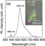
We identified three types of SFs by performing PL measurements. Figure 1 shows the PL spectra of the three types of SFs, and their PL images are inset. The luminescence at about 500–600 nm in the PL spectra is emitted from the substrates due to impurities in the substrates. The PL images suggest that the three types of SFs have triangular shapes. The PL spectra reveal luminescence at 389 nm, which corresponds to the 4H-SiC bandgap. This luminescence at 389 nm is emitted from the substrates and 4H-SiC parts of the epitaxial layers around these SFs. In addition, Figs. 1(a)–1(c) show the luminescence at 539, 457, and 483 nm, respectively. These luminescences indicate that the three types of SFs are (a) 3C inclusions, (b) 8H-SFs and (c)  -SFs.3,18) Thus, we found that these three types of SFs were generated in the C-face epitaxial layers with a 1° off-angle. Other types of SFs were rarely generated and their densities were much lower than those of 3C inclusions, 8H-SFs and
  -SFs. In the following sections, we describe how we observed 3C inclusions, 8H-SFs and
  -SFs, and investigated the dependence of the growth conditions on their densities to discuss the important factors related to decreasing these defects.
Download figure:
Standard image High-resolution image
Download figure:
Standard image High-resolution image
Fig. 1. PL spectra of three types of SFs; (a) 3C inclusion, (b) 8H-SF, and (c)  -SF, and their PL images (inset figures).
Download figure:
Standard image High-resolution image3.3. Discussion of 3C inclusion-density reduction
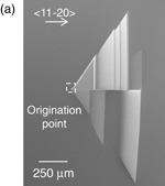
We observed a 3C inclusion using a SEM to look for the presence of some kind of trigger at its origination point. Figures 2(a)–2(c) show a surface SEM image of the 3C inclusion, a magnified bird's eye view of its origination point, and a cross-sectional bird's eye view of the origination point, respectively. Figure 2(a) shows that part of the 3C inclusion is brighter than that of the area without SFs presumably due to the difference in the carrier concentration.19) It is clear that there is a particle at the origination point of the 3C inclusion as shown in Fig. 2(b). Figure 2(c) indicates that the 3C inclusion is generated from the particle. The brightness of the particle is the same as that of the 3C inclusion part, which emits the 3C-SiC luminescence shown in Fig. 1(a). Moreover, other reports show that the cause of 3C inclusions is 3C-SiC particles.3,20) Therefore, the particle must be a 3C-SiC polytype.
Download figure:
Standard image High-resolution image
Fig. 2. (a) Surface SEM image of a 3C inclusion, (b) a magnified bird's eye view of its origination point, and (c) a cross-sectional bird's eye view of the origination point.
Download figure:
Standard image High-resolution imageWe estimated the points at which the 3C inclusions were generated by multiplying tangent 1° by the length along the ![$[11\bar{2}0]$](https://content.cld.iop.org/journals/1347-4065/54/4S/04DP04/revision1/SS14078if009.gif) direction obtained from the PL images. The generation points were defied as points located less or more than 1 µm from the interface between the substrates and epitaxial layers. The 3C inclusions were considered to be generated near the interface between the substrates and epitaxial layers when the generation points were located less than 1 µm from the interface, and to be generated during epitaxial growth when the generation points were located more than 1 µm from the interface. Figure 3 shows a schematic drawing of this method for estimating the generation point. As a result, both types of 3C-inclusions were observed, which suggests that the 3C inclusions were caused by 3C-SiC particles which were present on the substrates prior to epitaxial growth, or which had fallen on the substrates during epitaxial growth from the inside walls of the chemical vapor deposition reactor.
direction obtained from the PL images. The generation points were defied as points located less or more than 1 µm from the interface between the substrates and epitaxial layers. The 3C inclusions were considered to be generated near the interface between the substrates and epitaxial layers when the generation points were located less than 1 µm from the interface, and to be generated during epitaxial growth when the generation points were located more than 1 µm from the interface. Figure 3 shows a schematic drawing of this method for estimating the generation point. As a result, both types of 3C-inclusions were observed, which suggests that the 3C inclusions were caused by 3C-SiC particles which were present on the substrates prior to epitaxial growth, or which had fallen on the substrates during epitaxial growth from the inside walls of the chemical vapor deposition reactor.
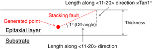
Fig. 3. Schematic drawing of method for estimating the SF generation point.
Download figure:
Standard image High-resolution imageWe investigated the relationship between the in-situ H2 etching depth and 3C-inclusion density, because we assumed that the particles which were present on the substrates before epitaxial growth were removed by in-situ H2 etching. Figure 4 shows the 3C-inclusion density for the in-situ H2 etching depth. The red and blue bars indicate the density of the 3C inclusions generated near the interface between the substrates and epitaxial layers and during epitaxial growth, respectively. The C/Si ratio was 2.0. The 3C-inclusion density is approximately 0.5 cm−2 when the in-situ H2 etching depth exceeds 0.4 µm, although the density is 1.6 cm−2 when the depth is 0.1 µm. An in-situ H2 etching depth of over 0.4 µm is needed to remove the 3C-SiC particles which were present on the substrates before epitaxial growth.
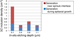
Fig. 4. Relationship between 3C-inclusion density and in-situ H2 etching depth.
Download figure:
Standard image High-resolution imageIn addition, we investigated the relationship between the C/Si ratio and the 3C-inclusion density; however, the 3C-inclusion density was not changed by varying the C/Si ratio from 0.8 to 2.0. As reported for Si-face epitaxial growth with a low off-angle of less than 1°, the 3C inclusion density increases as the C/Si ratio increases because 3C-SiC nucleation occurs due to the short diffusion length of adatoms and the wide terrace width caused by step bunching generation.11,21,22) Compared with the reported Si-face epitaxial growth, the 3C-inclusion density on the C-face did not increase as the C/Si ratio increased. With C-face epitaxial growth, we consider that 3C inclusions, which were attributed to 3C-SiC nucleation occurred by the wide terrace width, were not generated since the terrace width was not increased by the suppression of step bunching because of its lower surface energy compared with a Si-face.8)
The 3C-inclusion density was not affected by the growth parameters but was affected by the chamber conditions. The 3C-inclusion density decreased when in-situ H2 etching depth exceeded 0.4 µm because it removed the 3C-SiC particles that were present on the substrates before epitaxial growth.
3.4. Discussion of 8H-SF and  -SF density reduction

We observed an 8H-SF and a  -SF using SEM, but did not observe any particles at their origination points in contrast to the 3C inclusions. Using the method described in Sect. 3.3, we found that almost all these SFs were generated near the interface between the substrate and epitaxial layer. In addition, the densities of both the 8H-SF and
  -SF did not depend on the growth parameters of either the in-situ H2 etching depth or the C/Si ratio.
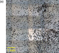
It is possible that defects in substrates cause SFs in epitaxial layers. To investigate the dependence of the crystal quality of the substrates on these SF densities, we grew two epitaxial layers under the same conditions (in-situ H2 etching depth of 0.4 µm and C/Si ratio of 2.0) on substrates cut from different boules. Figures 5(a) and 5(b) show microscopic images of the Si-face substrates cut from two different boules after KOH etching. Dislocations on the Si-face SiC materials reveal etch pits after KOH etching.23) The etch pit density obtained from Figs. 5(a) and 5(b) is 4.1 × 10³ and 8.3 × 103 cm−2. It means that the dislocation density of the substrate shown in Fig. 5(b) is slightly higher than that of the substrate shown in Fig. 5(a). Moreover, the substrate shown in Fig. 5(a) has many high dislocation density areas unlike the substrate shown in Fig. 5(b), which has evenly-distributed dislocations. We grew epitaxial layers on these C-face substrates. The epitaxial layer grown on the substrate shown in Fig. 5(a) had an 8H-SF density of 0.38 cm−2 and a  -SF density of 0.43 cm−2. The epitaxial layer grown on the substrate shown in Fig. 5(b) had an 8H-SF density of 0.05 cm−2 and a
  -SF density of 0.01 cm−2. The 8H-SF and
  -SF densities changed depending on the boules used as substrates even under the same growth conditions. We believe that these SF densities were affected by the dislocation distribution of the substrates.
Download figure:
Standard image High-resolution image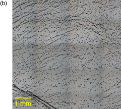
Fig. 5. Microscopic images of Si-face substrates cut from two different boules after KOH etching.
Download figure:
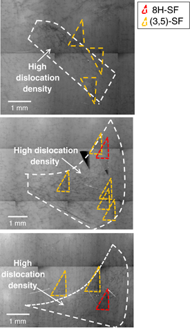
Standard image High-resolution imageWe investigated the dislocations of a 9 µm epitaxial layer grown on the substrate shown in Fig. 5(a) around these SFs by using PL images detected using a long-pass (>750 nm) filter. Figure 6 shows the PL images of three positions of the epitaxial layer where 8H-SFs and  -SFs are generated at relatively high densities. 8H-SFs and
  -SFs are outlined with red and orange dashed lines, respectively. The triangular defects with no marks are 3C inclusions. Both the epitaxial layer and the substrate were excited because we employed 295–370 nm Hg-lamp excitation through a bandpass filter and the penetration depth was approximately 100 µm at 370 nm.24) The dislocations in the substrates and epitaxial layers have dark and bright spots, respectively, in PL images detected using this long-pass filter.25–28) However, the bright spots are not visible because of the low magnification measurement and weak luminescence of the dislocations in this study. In these figures, many dark spots are observed that correspond to dislocations in substrates. Areas with lower and higher dislocation densities are separated by a white dashed line and the areas inside the white dashed lines are the high dislocation density areas. The 8H-SFs and
  -SFs are generated in or near the high dislocation density areas on the substrate. It is possible that the high dislocation density areas of the substrates rather than the dislocations themselves cause the 8H-SFs and
  -SFs. It has been reported that nucleation of multiple 2D islands on the terraces may lead to the formation of faulted Si-C bilayers and in-grown SFs, and the nucleation is not connected to any other defect, inclusion, particulate, or any type of heterogeneity in the epitaxial layer or the substrate.29) In addition, it has been reported that a cluster of threading dislocations exist near the starting point of the 8H-SFs and such irregularity can increase the chance of a polytype error during epitaxial growth.30) Therefore, we think that the nucleation of multiple two-dimensional islands occurred in or near the high dislocation density areas because the diffusion length of adatoms became short as a result of the increase in dangling bonds. Further investigation of the 8H-SF and
  -SF generation mechanism is needed but it is important to suppress generation of the high dislocation density areas on substrates if we are to reduce 8H-SF and
  -SF densities.
Fig. 6. PL images detected using a long-pass (>750 nm) filter of epitaxial layers, which had grown on the substrate in Fig. 5(a), around the 8H-SF and  -SF generation positions. 8H-SF and
  -SF are outlined with dashed red and orange dashed lines, respectively.
Download figure:
Standard image High-resolution image
4. Conclusions
We grew epitaxial layers on 4H-SiC C-face substrates with a 1° off-angle and discussed important factors related to reducing SF density. We found that 3C inclusions, 8H-SFs and  -SFs were generated in grown epitaxial layers. The cause of the 3C inclusion was 3C-SiC particles which were present on the substrates before epitaxial growth, or which had fallen on the substrates during epitaxial growth from the inside walls of the chemical vapor deposition reactor. An in-situ H2 etching depth of over 0.4 µm is needed to reduce the 3C-inclusion density. In addition, we found that the high dislocation density areas of the substrates rather than the dislocations themselves cause the 8H-SFs and
  -SFs. It is important to suppress generation of the high dislocation density areas on substrates as regards reducing the 8H-SF and
  -SF densities.
Acknowledgment
This work is supported by the Novel Semiconductor Power Electronics Project Realizing Low Carbon Emission Society under the New Energy and Industrial Technology Development Organization (NEDO).