
Abstract
We report the observation of spontaneous and stimulated Raman scattering in a silica-cladded silicon photonic crystal (PhC) waveguide (WG) with modified holes. Spontaneous Raman scattering in the WG was enhanced when the Stokes wavelength was approached to the bandedge of a WG mode. A maximum enhancement up to ∼5 times was obtained in the present work. At a Stokes wavelength in the lower group velocity region, nonlinear increase of the Stokes power as the pump power, a clear indication of the onset of stimulated Raman scattering, was observed. Moreover, Raman amplification with an external signal beam was also demonstrated. On–off gain becomes small as the Stokes wavelength gets away from the bandedge of the WG mode. These are the first observations of Raman scattering effects in silica-cladded silicon PhC structures.
Export citation and abstract BibTeX RIS
1. Introduction
Silicon photonics is an essential technology for realizing the integration of photonics with complementary metal–oxide–semiconductor (CMOS) electronics on single silicon substrate.1,2) The development of silicon-based photonic devices such as waveguides, modulators, and photodetectors have paved the way for future smaller and cheaper photonic integrated circuits (PICs). However, the realization of efficient silicon-based light sources remains challenging due to the intrinsic indirect electronic band-gap of crystalline silicon. Nonlinear optical effects including stimulated Raman scattering can provide another route to achieve laser oscillation or light amplification in pure silicon. In the past decades, pulsed and continuous-wave silicon Raman amplifiers3–9) and Raman lasers10–13) have been successfully demonstrated using silicon rib and wire waveguides (WGs). However, for sufficient light amplification or lasing operation, silicon waveguides longer than 2 cm and pump powers larger than 100 mW are necessary.
Photonic crystal (PhC) WGs14–17) are expected as key structures to overcome the aforementioned issues. The advantages of small cross section area and low group velocity of propagating modes in PhC WGs can enhance the light-matter interaction, which can dramatically enhance the Raman scattering and Raman gain.18,19) Consequently, the device length could be shortened and the required pump power could be reduced. Since the first experimental report on spontaneous Raman scattering in a GaAs PhC WG,20) Raman scattering effects in PhC WGs has been investigated using AlGaAs-based air-bridge slabs.21,22) For the aforementioned purposes, various research works on Raman scattering in silicon PhC structures have been also intensively conducted recently. In silicon air-bridge PhC WGs, enhanced spontaneous Raman scattering due to the slow light effect23) and stimulated Raman scattering24) have been observed. Recently, an ultra-compact Raman laser with low threshold power has also been demonstrated using a high-Q air-bridge PhC nanocavity.25) Most studies of Raman scattering on PhCs make use of the air-bridge structure. In comparison, silica-cladded structures have superior mechanical and thermal stability. However, there are still no reports of Raman scattering effects in silica-cladded PhC WGs. Observation of spontaneous Raman scattering in silicon PhC WGs on silica but with an upper air layer was reported before.26) The symmetric confinement of electromagnetic fields in silica-cladded structures is preferable. The symmetric nature allows to separate TE-like and TM-like modes definitely, which enable to suppress the mode coupling loss of photonic components in PhC structures. Symmetric mode distributions would be beneficial for better coupling from external fibers.
Here, to the best of our knowledge, we report the first observation of Raman scattering effects in silica cladded PhC structures. Enhanced spontaneous Raman scattering and stimulated Raman scattering were demonstrated in silica-cladded PhC WGs with modified holes. Raman amplification with an on–off gain of ∼2 dB was also observed. This is also the first measurement of on–off gain of Raman amplification with an external signal beam in any types of PhC WGs.
2. Sample structures and experimental setup
We firstly designed a silica-cladded PhC WG structure with modified holes based on our previous research.27) Silica-cladded PhC WGs have aforementioned advantages. On the other hand, the higher refractive index of silica than air, which lower the frequency of light line than that for air-bridged structures, sacrifices the design and operation flexibility. The frequencies of waveguide modes also change depending on their field distribution and polarization. Therefore, some of the designs in the previous works using air-bridge PhC WGs may not work effectively in silica-cladded structures. For instance, the W0.66 WG in Ref. 25 is not suitable for silica-cladded structures because the pump frequency will be above the light line. Thus, careful designs are needed for silica-cladded structures.
Figure 1(a) illustrates the designed structure. Here we set the width parameter x = 0.7, lattice constant a = 460 nm, the hole radius r = 0.32a, slab thickness H = 210 nm, modified hole center position D = r, and modified hole radius r2 = 0.8r. The waveguide is parallel silicon crystal orientation of [110]. Similar to the structures discussed in Ref. 27, this structure was designed so that the PhC WG can support two symmetric transverse electric (TE)-like slow-light modes with a frequency separation of ΔωR = 2π × 15.6 THz (the Raman shift of silicon) at around the Brillouin zone edge. The frequency separation corresponds to the energy of the zone-center optical phonon in silicon. For the first-order Raman scattering discussed in this work, only the zone-center optical phonons can contribute dominantly due to the momentum conservation.28) These guided modes are intended to be used as the pump and Stokes waves.

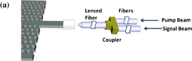
Fig. 1. (a) Illustration of a designed silica cladding PhC WG with modified holes. (b) SEM images of a fabricated PhC WG. The inset shows the magnified view around the connection part between the PhC WG and an access wire WG. (c) Schematic of light coupling configuration. Light beams couple in and out devices through lensed fibers. Access wire WGs allow to connect the PhC WG to chip boundary. Spot size converters are integrated at the entrance and exit of the access WGs for improving coupling efficiency.
Download figure:
Standard image High-resolution imageThe designed structure was fabricated by CMOS compatible processes through a foundry service. The scanning electron microscope (SEM) image of one of the devices is shown in Fig. 1(b), which was taken after removing the cladding silica by a wet etching process. The WG length L is 184 µm. The modified holes connected each other because of over-exposure. Unfortunately, the design was not ideally reproduced in the real devices. However, as shown below, a waveguide mode is still available for investigating enhanced Raman scattering in the silica-cladded PhC WG.
We performed optical characterizations of the device by coupling light beams to the PhC WGs from lensed fibers as shown in Fig. 1(c). Access wire WGs were attached to the PhC structure in order to connect the entrance and exit of PhC WGs to chip boundaries [see also Fig. 1(b)]. Spot size converters were also introduced in our devices for improving coupling efficiency between the external lensed fibers and the access wire WGs. To obtain the linear transmittance spectra, we used wavelength tunable continuous wave (CW) laser and measured the output power collected by the lensed fiber by using a power meter. The transmittance was evaluated by calculating the ratio of the measured output power to the input power. In order to avoid any nonlinear optical effects, the transmittances were measured under a low input power of 0 dBm. Note that the input and output powers in this study are measured at the "input" and "output" points (red balls) as shown in Fig. 1(c). In the Raman scattering experiments, the output from a CW laser was amplified by a fiber-based optical amplifier first and was used as the pump source, and the Stokes signal was collected by the lensed fiber and was detected by an InGaAs photodiode array through a monochromator. We used an additional weak CW laser as a signal beam for Raman amplification measurements. For details, see Sect. 3.3 and Fig. 4.
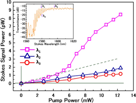
Fig. 4. Pump power dependence of Stokes signal power for various Stokes wavelengths λ1 = 1579.5 nm (pink squares), λ2 = 1582.1 nm (cyan triangles), and λ3 = 1596.0 nm (red circles). Inset: Transmittance spectrum in the wavelength range of 1560–1620 nm. The arrows indicate the wavelength of λ1, λ2, and λ3.
Download figure:
Standard image High-resolution image3. Results and discussion
3.1. Transmittance spectrum
The transmittance spectrum of the devices for TE-like polarization is shown in Fig. 2. We redrew the outline of the PhC patterns based on the SEM images [Fig. 1(b)] and calculated the corresponding photonic band diagram, which is also shown in Fig. 2. The measured transmittance is low around the wavelength range from 1400 to 1460 nm because the WG modes are above the light-line, which means the losses in the out-of-plane direction is increased. In addition, this region also overlapped with the slab modes, which is indicated by the grey-colored region in the band diagram in Fig. 2. The observed stop-band around 1550 nm agrees well with the calculated mode-gap. This clear opening of mode gap indicates the difference of the measured structure from the simple wire waveguide. The group index (ng) of 10.5 was estimated at 1560 nm, near the band edge, from the band structure in Fig. 2. For comparison, we calculated ng of ∼4 at the same wavelength for a wire WG with a width of 320 nm, which corresponds to the average width of the undulated central wire of the PhC WG. This also differentiates the PhC WG from such a simple wire WG. The high transmittance regions around wavelengths of 1470 to 1540 nm and 1575 to 1630 nm correspond to the PhC WG guiding modes. These guiding modes have symmetric field distribution as discussed in Ref. 27. We intended to use the bandedge regions of these modes for pump and Stokes waves because large enhancement of Raman scattering is expected due to the simultaneous slowdown of the group velocities both for pump and Stokes waves. Due to the imperfection in the fabrication [see Fig. 1(b)], the wavelength difference of the two bandedges cannot match the Raman shift in silicon in the real device. Therefore, the pump wavelength must be operated at around 1460 nm so that the Stokes wavelength operated at low group velocity region (around 1580 nm). At 1460 nm, the waveguide modes are located at around or even above the light-line not close to a bandedge, where large reduction of group velocity occurs. Thus, strong slow light effect as those in the designed structure is not likely to be observed. However, the Stokes wavelengths can be located in the low group velocity regions of a guiding mode. Thus, the slow-light effect for the Stokes wave is still expected to be observed. In this study, we investigated Raman scattering whose Stokes wavelengths located at around the bandedge of the first guiding mode corresponding to the high transmission region ranging from 1575 to 1630 nm.

Fig. 2. Transmittance spectrum for TE polarization and the corresponding calculated band diagram by taking the parameters from the SEM images.
Download figure:
Standard image High-resolution image3.2. Wavelength and pump-power dependences of Raman scattering
We first measured the Stokes signal generated by Raman scattering from the CW pump beam. Figure 3 summarizes the results of wavelength dependences of Stokes power. For illustrating the spectral region investigated here, in Fig. 3(a), we again plotted the transmittance spectra around the operation wavelength regions of pump (1430–1520 nm) and Stokes waves (1544.9–1650.5 nm) simultaneously. A vertical line connecting the top and bottom axes gives us a pair of pump and Stokes wavelengths, whose difference matches the Raman shift of silicon (ΔωR = 2π × 15.6 THz). In the spectrum for Stokes wave (brown curve), clear interference fringes are observed. The interference fringes were originated from the mode mismatch between access wire WGs and the PhC WG.
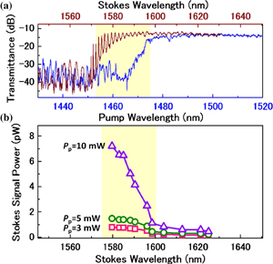
Fig. 3. (a) Transmittance spectra for TE polarization around the pump wavelength range from 1430 to 1520 nm (blue curve) and around the Stokes wavelength range from 1544.9 to 1650.5 nm (brown curve). (b) Stokes signal power as a function of Stokes wavelength under pump power of 3 mW (red squares), 5 mW (green circles), and 10 mW (purple triangles).
Download figure:
Standard image High-resolution imageFigure 3(b) plots the Stokes powers measured at various pump powers of 3, 5, and 10 mW as a function of the Stokes wavelength. In these measurements, we carefully chose the pump wavelengths so that the corresponding Stokes wavelengths located at the interference peaks in the linear transmittance spectrum. For all three pump powers, Stokes power is increased when the wavelength approaches to the bandegde of the guiding mode for the Stokes wave although the transmittance of the mode for the pump becomes low (see the shadowed region in Fig. 3). At the pump power of 3 mW, the Stokes power measured at 1579.5 nm was about 5 times stronger than that at 1624.9 nm. At this pump power, only spontaneous Raman scattering is likely to occur (see also Fig. 4 and related discussions). The large difference in the transmittance of the pump waves over the measured spectral range makes it difficult to compare Raman scattering efficiencies at these two wavelengths directly from the experiment. However, slow-light effect for the Stokes wave can be considered as one of the origins for the enhancement of spontaneous Raman scattering in this range. In the present experiment, due to the limitation of the emission wavelength of our pump laser, we could measure the Stokes signal longer than 1579.5 nm. A larger enhancement of spontaneous Raman scattering is also expected in the Stokes wavelengths from 1568 to 1579 nm, where the group velocity for the Stokes wave becomes smaller.
The enhancement of Raman scattering in the lower group velocity region of the Stokes wave (i.e., at around 1580 nm) is much pronounced for higher pump powers, particularly at 10 mW. This result suggests that stimulated Raman scattering can take place at higher pump powers. For detailed investigations, we measured the Stokes signal power at different wavelengths as a function of pump power. The results are shown in Fig. 4. The pump wavelengths were chosen as 1459.6, 1461.8, and 1473.7 nm. The corresponding Stokes wavelengths are λ1 (1579.5 nm), λ2 (1582.1 nm), and λ3 (1596.0 nm), which are located at a transmittance peak and valley wavelengths in the lower group velocity region, and a transmittance peak wavelength in a higher group velocity region, respectively, as shown in the inset of Fig. 4. As expected, the Stokes signal power in the λ1 case increased superlinearly when the pump power increased above ∼4 mW. This indicates the onset of stimulated Raman scattering. On the other hand at lower pump powers, only spontaneous Raman scattering occurs and the Stokes intensity increased linearly as shown in the eye guide (broken line). In contrast, in the λ3 case, even with higher transmission of the pump compared with the λ1 case, the Stokes power only increased linearly since the Raman scattering efficiency in the λ3 case is lower than that in the λ1 case as shown in Fig. 3(b). No nonlinear increase was observed also in the λ2 case although the wavelength is located very close to λ1. This can be attributed to the weaker confinement of Stokes photons because λ2 located at a valley point in the interference.
3.3. Raman amplification
Utilizing the stimulated Raman scattering, it is possible to achieve amplification of a signal beam, which is simultaneously coupled to a silicon waveguide with the pump beam.3,4) In this experiment we used a coupler to combine the pump beam with the signal beam at the corresponding Stokes wavelength as shown in Fig. 5(a). In order to clearly understand the experiment conditions, here, we define three observed powers as Ps-off,p-on, Ps-on,p-off, and Ps-on,p-on. The measured integrated power over the Stokes line when only the pump beam is on is defined as Ps-off,p-on. This contains the Stokes signals created only by the pump beam. On the other hand, Ps-on,p-off is defined as the measured integrated power when only the signal beam is on. Thus, Ps-on,p-off is the transmitted power of the signal beam through the WG. Finally, Ps-on,p-on denotes the measured integrated power when both signal and pump beams are on. This contains the contributions from Raman scattering induced not only by pump but also by simultaneous existence of pump and signal. Thus, if the Raman gain occurs, Ps-on,p-on should be larger than Ps-off,p-on + Ps-on,p-off. Here, we define Raman on–off gain as

To clearly see the signal amplification effect, this on–off gain excludes the contribution of Raman scattering signal created solely by the pump beam (see the numerator).
Download figure:
Standard image High-resolution image
Fig. 5. (a) Illustration of the input configuration for Raman amplification experiments. Pump and Stokes beams are combined to the input lensed fiber by a coupler. Thus, pump and Stokes beams could be injected into devices simultaneously. (b) Raman on–off gain Gon–off as a function of pump power for various Stokes wavelengths, λ1 (purple squares), λ2 (blue triangles), and λ3 (orange circles) are shown.
Download figure:
Standard image High-resolution image
In Fig. 5(b), the Gon–off as a function of pump power at different operation wavelengths were plotted. The pump and signal laser of the amplification experiments were both operated under CW condition. The input signal power was kept at 15 pW. Within the pump power range used in the present experiments, the maximum Gon–off as high as 1.5 dB was obtained in the λ3 case. On the other hand, in the λ1 case, the maximum Gon–off reached up to 2.6 dB even with the lower transmittance of the pump than in the λ3 case. This difference in Gon–off reflects the difference of slow-light effect in part. Devices, where the pump waves below the light line are available, would enable to investigate the slow light effect on Gon–off in more detail. This would be our one of future works.
4. Conclusions
We observed spontaneous and stimulated Raman scattering in silica-cladded silicon PhC WGs with modified holes. The slow light enhancement of spontaneous Raman scattering was observed. In the present experiment, 5-times enhancement in the Stokes signal power was obtained at a Stokes wavelength close to the band edge, i.e., the low group velocity region, of a guiding mode in the PhC WG, compared with the measured Stokes power at a wavelength with higher group velocity. At a Stokes wavelength in the lower group velocity region, the Stokes signal power showed nonlinear increase as the pump power increased. This nonlinear increase indicated the onset of stimulated Raman scattering in the silica-cladded PhC WG Furthermore, Raman amplification with an external signal beam was also demonstrated. These are the first observations of Raman scattering effects in silica-cladded silicon PhC structures. Our results show the possibility of silica-cladded PhC structures for Raman amplifier and lasers in the future PICs or in other applications.
Acknowledgements
This research is supported by the Japan Society for the Promotion of Science (JSPS) through its Funding Program for World-Leading Innovative R&D on Science and Technology (FIRST Program) and the Project for Developing Innovation Systems of the Ministry of Education, Culture, Sports, Science and Technology (MEXT).