
Abstract
Non-evaporable getter (NEG) thin films based on alloys of transition metals have been studied by various authors for vacuum control in wafer-level packages of micro electro mechanical systems (MEMS). These materials have typically a relatively high activation temperature (300–450 °C) which is incompatible with some temperature sensitive MEMS devices. In this work we investigate the potential of Au/Ti system with a thin or ultrathin non oxidizable Au layer as a low activation temperature getter material. In this bilayer system, gettering activation is produced by thermal outdiffusion of titanium atoms through the gold film. The outdiffusion kinetics of titanium was modelled and characterized by scanning electron microscopy (SEM), X-ray photoelectron spectroscopy (XPS), and Rutherford backscattering spectrometry (RBS) at various temperatures. Results confirm that Au/Ti bilayer is a promising getter material for wafer-level packaging with an activation temperature below 300 °C for 1 h annealing time.
Export citation and abstract BibTeX RIS
1. Introduction
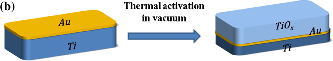
Many microelectromechanical systems (MEMS) such as resonant devices, microbolometers, RF switches and other ones need to be packaged under sustainable vacuum to reach and maintain high performances.1) Vacuum wafer-level packaging can be successfully achieved by combining wafer bonding with highly hermetic sealing rings and vents, vents sealing by deposited layers, and pre- or post-baking at elevated temperature for oxide reduction and outgassing.2) Such getter-free vacuum packaging processes often require very high temperatures (up to 950 °C) which are compatible with a limited number of MEMS devices only. A more versatile and common way to get a low and sustainable pressure level in vacuum packaging is to integrate films of non-evaporable getter (NEG) materials in the package cavity to absorb gases released by outgassing or arising from leaks.3) Most of investigated NEG films are binary, ternary or quaternary sputtered alloys of transition metals (Zr, V, Co, Ti, etc.) with optional additives. They are activated by bulk dissolution of their passivating oxides by thermal annealing under vacuum to expose reactive metals at the surface [Fig. 1(a)]. This requires relatively high temperatures (300–500 °C)3–8) and/or very long annealing time,9,10) which might be detrimental to the encapsulated device. In recent years many investigations were performed to reduce the activation temperature of NEG alloys films and an activation temperature of 240–250 °C was demonstrated recently for a 2 h annealing time.11,12) Nevertheless these NEG alloys films have also as drawback the need of uncommon and complex sputtering targets or the need of a co-sputtering equipment. In addition, the incorporation of sputtering gas atoms (usually argon) can degrade the getter film sorption properties and can be released during the bonding, thus limiting the vacuum level that can be reached and maintained.13) An alternative is to use single layer or multilayer getters.14–17) As for alloys, single getters also require a high temperature vacuum annealing to regenerate an active surface and their sorption properties can be degraded by surface contamination during processing steps. For example, in the case of Ti getter films an activation temperature of 450 °C is required to reach a full getter sorption capacity.16) It was found that this activation temperature can be reduced to 375 °C for an annealing time 1 h by using a Cr sublayer16) but the temperature still remains too high for the targeted applications. We proposed in the past the use a titanium film passivated by a thin film of gold as a getter for vacuum wafer-level packaging and preliminary experiments were performed with success.15) Gold was chosen as it is a non oxidizable metal with a low surface reactivity and a high chemical resistance. The activation of such Au/Ti getter is obtained by out diffusion of Ti atoms through this protecting layer [Fig. 1(b)]. This type of multilayer getter was also investigated by Tenchine et al.16) in the case of Pt (60 nm)/Ti film. An activation temperature of 450 °C was required to get the same sorption capacity than a single Ti film. Finally Au/Ti and Ni/Ti getters were also investigated very recently by Chimbaram et al.17) who claimed that Ni is a better candidate than Au, but an activation temperature of 400 °C for 90 min was needed.

Download figure:
Standard image High-resolution image
Fig. 1. Conventional method for getter activation (a) and proposed method (b).
Download figure:
Standard image High-resolution imageIn this paper the thermal activation of Au/Ti getter is investigated in details by various techniques with the purpose of reducing the activation temperature below 300 °C by reducing the Au passivation layer thickness.
2. Experimental methods
The titanium and gold films have been deposited by e-beam evaporation to avoid rare gas contamination. Prior to deposition, the Si(100) wafers were ultrasonically cleaned in acetone and ethyl alcohol and then dipped into piranha and BHF solutions to remove organic residues and native oxide respectively. After each step, the wafers were rinsed using deionized water and finally blow-dried with nitrogen. Immediately after cleaning, the substrates were introduced in the evaporation set-up to limit surface oxidation. A 100-nm-thick titanium layer and a 2–20-nm-thick gold layer were then successively deposited, by using the deposition parameters listed in Table I. After deposition, the films were annealed in a furnace in N2 or vacuum with variable annealing temperatures and times. The oxygen gettering ability of the layers was asserted from surface oxidation due to the presence of oxygen and water vapour in the annealing gas. In case of N2 and primary vacuum these traces are estimated to be in the range of a few ppm to a few tens ppm, corresponding to partial pressures of oxidizing species in the range of a few 10−3 to a few 10−2 mbar. These values are similar to the ones found in wafer-level vacuum packages. The surface morphology and chemical bonds have been respectively characterized by scanning electron microscopy (SEM; Hitachi SU8000), and by X-ray photoelectron spectrometry (XPS). An Al Kα source monochromatized at 1486.6 eV and a hemispheric analyser working at a pass energy of 50 eV were used for XPS measurements. As the escape depth is around 2 nm for ∼1 keV photoelectrons corresponding to Ti 2p and O 1s peaks, the analysed depth is in the range of 5–6 nm. For 20-nm-thick Au films, Rutherford backscattering spectrometry (RBS) has been used for the investigation of interdiffusion after annealing.
Table I. Deposition conditions of Au/Ti bilayers.
| Material | Thickness (nm) | Deposition rate (nm/s) | Power (kW) | Pressure (mbar) |
|---|---|---|---|---|
| Ti | 100 | 0.864 | 1.3 | 2.9 × 10⁻⁸ |
| Au | 2 | 0.084 | 1.0 | 3.1 × 10⁻⁸ |
| Ti | 100 | 0.973 | 1.3 | 3.2 × 10⁻⁷ |
| Au | 5 | 0.092 | 1.0 | 4.7 × 10⁻⁷ |
| Ti | 100 | 0.93 | 1.8 | 6.0 × 10⁻⁸ |
| Au | 20 | 0.099 | 1.0 | 8.0 × 10⁻⁸ |
3. Results and discussion
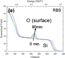
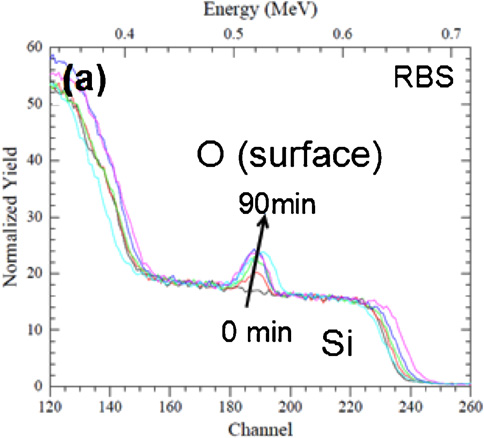
The RBS spectra of Au (20 nm)/Ti (100 nm) samples annealed at 380 °C in N2 show the presence of an oxidized titanium surface layer for annealing times larger or equal to 15 min. When increasing the annealing time, the concentration of oxygen and titanium at the surface increases significantly (Fig. 2). Likewise, increasing the annealing temperature also leads, as expected, to an increase of the amount of these elements accumulated at the free surface. This is illustrated in Fig. 3 where the kinetics of surface concentrations of Ti and O recorded at 380 and 415 °C were compared. These results demonstrate the diffusion of the titanium through the gold layer followed by its oxidation. It is worth of emphasizing that this Ti oxidation provides an additional driving force for diffusion, as it has been showed for Co.18) Indeed, diffusion would expect to be rapidly limited when pure Ti is both above and below the Au layer.
Download figure:
Standard image High-resolution image
Fig. 2. RBS spectrum: oxygen (a) and titanium (b) peaks for different annealing times at 380 °C (15 min steps between each curve).
Download figure:
Standard image High-resolution image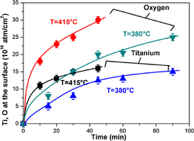
Fig. 3. Titanium and oxygen surface concentrations as a function of annealing time at 380 °C.
Download figure:
Standard image High-resolution imageThese experiments were performed with a 20-nm-thick Au layer and at relatively high temperature to better evidence the interdiffusion phenomena but as mentioned above, a lower activation temperature is desirable for wafer-level vacuum packaging applications. We therefore studied theoretically and experimentally the effect or a lowering of the gold thickness.
Semi-analytical simulations have been performed to quantify the diffusion of Ti through the Au layer. The following simplifying assumptions have been made: (i) Ti atoms diffuse through gold uniformly in the plane (one-dimensional geometry), (ii) the diffusion coefficient of Ti atoms inside Au is considered as independent of their concentration in the Au film, (iii) Ti atoms arriving at the outside surface of Au are immediately oxidized (diffusion well). To simplify the calculation, we neglected the diffusion of Au in Ti and we used the same initial concentration c0 for both materials (5.7 × 10²² atoms/cm3). In the modelling, we defined the coordinate origin at the Au/Ti interface and called x0 the initial thickness of Au. The diffusion model is based on Fick's second law:

Ti and Au concentrations evolution is thus supposed to follow an error function between x = 0 and x = xL (Fig. 4)


The total Au quantity remaining constant, i.e.,

The value xL thus corresponds to the distance between pure titanium and titanium oxide, D is the diffusivity of Ti in Au and c0 the initial concentration. At the initial stage, xL is equal to x0, i.e., the thickness of deposited gold and the layers are homogenous [Figs. 4(a) and 4(b)]. Due to the Kirkendall effect, atomic interdiffusion occurs during annealing. Once titanium reaches the gold surface, it immediately oxidizes and forms a TiOx surface layer [Figs. 4(c) and 4(d)]. The key-factor of the diffusion phenomenon is the diffusion length ( ).
).
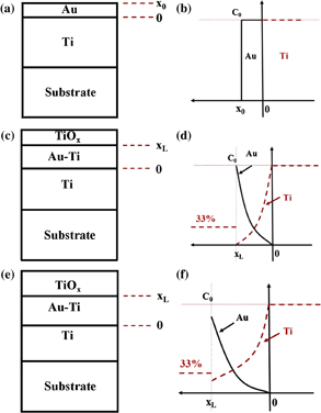
Fig. 4. Diffusion model in the as-deposited state (a, b) and after interdiffusion (c, d then e, f).
Download figure:
Standard image High-resolution imageAs expected, the simulations show that for the same diffusion length, more efficient gettering ability is obtained by reducing the gold layer thickness, so is for the similar annealing temperature or time (Fig. 5). In other words the Au/Ti getter activation is predicted to be easier when the Au thickness is reduced.
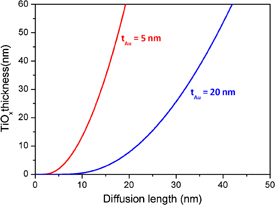
Fig. 5. Simulated TiO2 thickness as a function of Ti diffusion length for 5 and 20 nm Au films on Ti.
Download figure:
Standard image High-resolution imageAnnealing experiments of Au/Ti films with a 5-nm-thick Au layer were then performed to evaluate the validity of this simple model. Figure 6 compares the results of XPS surface analyses for samples covered with 5 and 20-nm-thick of gold. It shows that even for a gold thickness of 5 nm, no oxygen is detected before annealing. This demonstrates the protective ability of the gold layer and its integrity. After heat treatment in N2, high concentrations of titanium and oxygen are observed. The peaks of concentrations are associated with the presence of a superficial TiOx layer whose thickness increases with temperature and has a composition close to TiO2. After annealing at 200 °C for 1 h, only 53% of gold remains in the analysed volume for the Au (5 nm)/Ti (100 nm) sample, while it reaches 82% for a 20-nm-thick Au film, confirming thus the lowering of the activation temperature by using a thinner protective layer. As the annealing temperature increases, Au/Ti interdiffusion continues, and after annealing at 300 °C for 1 h, there is almost no gold remaining in the analysed volume for the Au (5 nm)/Ti (100 nm) sample, but still 42% in the Au (20 nm)/Ti (100 nm) sample. These temperatures are lower than the temperature (325 °C) reported by Sylwestrowicz,19) this suggests that the process is facilitated by diffusion through grain boundaries.

Fig. 6. Normalized variations of O 1s, Ti 2p, and Au 4f XPS peaks as function of 1 h N2 annealing temperature for Au (5 and 20 nm)/Ti (100 nm) samples.
Download figure:
Standard image High-resolution imageSEM cross-section images using both secondary electrons (SE) and backscattered electrons (BSE) detection show that the as-deposited gold films are smooth (Fig. 7). After annealing at 350 °C, the titanium oxide layer completely covers the buried gold film. These images allowed the measurement of the TiOx thickness as a function of the annealing temperature (Fig. 8). By fitting these values using the model presented previously, the diffusion coefficient D of Ti in Au was estimated. When thermally activated, D is express as

The extracted values, D0 = 4.7 × 10⁻¹¹ cm2/s and ΔE = 0.62 eV are in close agreement with the ones evaluated by Martinez,20) i.e., D0 = 5 × 10⁻¹¹ cm2/s and ΔE = 0.66 eV.

Fig. 7. SEM images of the cross-section of an Au (5 nm)/Ti samples in as deposited state (top) and after N2 furnace annealing at 350 °C for 1 h (bottom). Left: (SE) images. Right: BSE images.
Download figure:
Standard image High-resolution image
Fig. 8. Titanium oxide and Au–Ti thicknesses versus 1 h annealing temperature for Au (5 nm)/Ti (100 nm). Squares: experimental values extracted from SEM measurements; solid black line: fit with Ti diffusion model; solid red line: simulated Au–Ti thickness.
Download figure:
Standard image High-resolution imageWith increasing annealing temperature, the titanium diffuses in gold and the Au–Ti equivalent layer thickness, characterized by xL is predicted to increase [Figs. 4(e) and 4(f)]. After annealing at 350 and 400 °C for 1 h, xL values are respectively close to 15 and 20 nm, what are consistent with the cross-section SEM pictures.
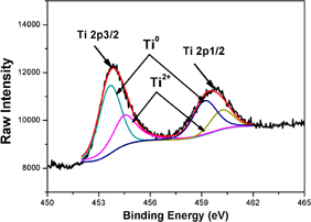
To try to further reduce the activation temperature, a sample covered with an ultrathin gold layer (2 nm) has been realized and the surface chemical bonds have been characterized by XPS. We observed the presence of an O 1s peak in the as-deposited sample, indicating a partial oxidation of the Ti layer. Peak deconvolution showed that 86% of the O 1s peak corresponds to bonding between Ti and O, the remaining 14% to the surface contamination. Figure 9 shows a zoom on the Ti 2p peaks. It confirms titanium oxidation: 65% of the Ti 2p3/2 peak at 453.64 eV, corresponds to Ti metal21) and 35% of the Ti 2p3/2 peak at 454.5 eV, corresponding to Ti2+.22) Thus a 2-nm-thick capping gold layer is not sufficient to protect the titanium layer, likely because it is not continuous and/or is porous.
Fig. 9. XPS Ti 2p peak of the as-deposited Au (2 nm)/Ti (100 nm) sample.
Download figure:
Standard image High-resolution image
Thermal treatments of Au (5 nm)/Ti (100 nm) in N2, primary vacuum (<1 mbar) and secondary vacuum (<10−8 mbar) have been compared. XPS analysis of the Ti peak (Table II) shows that the main contribution corresponds to TiO2 for N2 and low vacuum, the remaining part corresponding to Ti–C. After annealing in low vacuum, an important contribution of metallic Ti is observed, that corresponds to non-oxidized titanium after diffusion through the gold layer. It is to notice that the presence of a Ti–N peak, as well as CO, CO2, or N2 peaks highlight the gettering ability of other gases than oxygen. However, these peaks are only detectable and do not allow a realistic quantification. Four-probe resistivity measurements at room temperature showed that the sheet resistance of the film annealed under low vacuum slowly increases with time: 2.5 and 5% after 6 month for samples annealed at 300 °C-1 h and 400 °C-1 h, respectively. By transposition to gettering applications in MEMS cavities, these results show that reactive Ti can be exposed, firstly to pump gases in the cavity, and secondly to maintain the vacuum for a long time. Indeed, by estimating the TiOx layer thickness after annealing in N2 (5 nm after 300 °C/1 h) and considering that 50% of Ti remains metallic after annealing in high vacuum, the quantity of oxygen that can potentially be trapped by 1 cm2 of getter material is close to 1.3 × 10⁻⁸ mole i.e., 0.032 Pa.l.
Table II. XPS analysis of Ti peaks.
| Annealing condition | Ti 2p/Ti–O2 (%) | Ti 2p/Ti–C (%) | Ti 2p/Ti–O3/2 (%) | Ti 2p/Ti0+ (%) |
|---|---|---|---|---|
| Nitrogen 300 °C/1 h | 85 | 15 | Not detected | Not detected |
| Prim. vacuum (<1 mbar) 300 °C/1 h | 89 | 11 | Not detected | Not detected |
| Sec. vacuum (<10−8 mbar) 300 °C/1 h | 15 | 25 | 10 | 50 |
4. Conclusions
In this work, the interdiffusion in the Au/Ti system deposited by e-beam evaporation was investigated as a solution to produce a low activation temperature getter film. It was found that a 5-nm-thick Au film is sufficient to protect the underlying Ti film while a 2-nm-thick Au film is not a barrier for oxidation at room temperature. During annealing, the titanium diffuses through the gold layer and is fully oxidized if the surrounding gas contains a small partial pressure of oxygen. In case of annealing in a low vacuum, half of the surface Ti remained metallic, thus active. The titanium outdiffusion and oxidation were also observed for a thermal activation as low as 200 °C for 1 h. The diffusion parameters of Ti in Au (D0 = 4.7 × 10⁻¹¹ cm2/s and ΔE = 0.62 eV) extracted from a fit of our experimental results with a semi-analytical model are in fair agreement with other works. The gettering potential has been estimated to 1.3 mole/cm2 of oxygen for a film annealed in secondary vacuum at 300 °C/1 h and evidence for further reaction at room temperature has been found. The presence of adsorbed CO, CO2, and N2 in the film has been observed after annealing, but the techniques we employed were not able to quantify these elements. The Au/Ti system might be used as a low activation temperature getter material for vacuum wafer-level packaging provided that a sufficiently thin and continuous Au film is deposited. Future works will be devoted to a better understanding and quantification of post-reaction of activated getters at room temperature.
Acknowledgments
This work was supported by the French National Research Agency (ANR) in the frame of the PRESTIGE project and by the French Renatech network. The authors wish to thank the clean room staff and the process engineers and technicians of the Microsystems and Nanobiotechnologies department for their assistance.
Biographies

Ming Wu received the degree in communication engineering from the Wenzheng faculty of Soochow university in China, and the Master degree in micro and nano technology from Lille 1 university – Science and technology, at Lille in France. She is currently pursuing a Ph.D. (thesis) on the getter materials (Zr, Ti, V) at the IEF. Her current research is Study and integration of getter film for low temperature vacuum packaging of quartz resonators.

Johan Moulin is born in 1971. He received the M.S. and Ph.D. degrees in electrical engineering from the ENS de Cachan, France, in 1998 and 2001 respectively. He is associate professor at Université Paris Sud, Orsay since 2003 and his research activities are related to magnetic material for MEMS, magnetic-based microsensors and actuators, packaging for MEMS and getter materials. He has published more than 60 articles in review and conference proceedings.

Sébastien Lani received a BS degree and MS degree respectively in 2002 and 2004 in Chemical engineering from University Paris VI, France. He received a Ph.D. in physics in 2007 from the university Paris XI on "MEMS wafer level packaging" topics. After 2 post doc experiences in MEMS and NEMS fabrication and characterization, respectively at CNRS (France) and EPFL (Switzerland), he joined the CSEM as an R&D engineer to lead product development on optical MEMS.

Géraldine Hallais after a Master in microstructural analysis of materials, in 2000, she becomes process engineer and component reliability at ALCATEL. In 2005, she was manager of the materials analysis laboratory in ALCHIMER company for the studies of the metallic or polymers layers obtained by (electro) chemical grafting. In 2011, she becomes CNRS Engineer at the ENS during 2 years where she was in charge of the implement techniques of micro–nano manufacturing for microfluidic studies with the responsibility of a cleanroom. Now she works at the IEF on incorporation epitaxial of III–IV–V materials on Silicium and has the responsibility of the materials analysis.

Charles Renard received the Ph.D. degree in materials sciences from Denis Diderot University, Paris, France, in 2005. His Ph.D. work has been done at Alcatel-Thales III–V and dealt with antimonide/arsenide heterostructures for optoelectronic applications in the mid infrared. Then he spent two years as a post-doctoral fellow at the Institut d'Electronique Fondamentale (IEF), Orsay, where he was in charge of CVD growth of nanostructures for ultimate MOSFET. In 2008 he spent 6 months at IMEC, within the Ge III–V explore programme. Since 2008, he is scientist researcher at IEF and work on hybrid integration of IV–IV of III–V materials on Si.

Alain Bosseboeuf received the Ph.D. degree in Physics from university Paris-Sud (Orsay) in 1989. Since 1983, he is a full-time CNRS researcher in Institut d'Electronique Fondamentale where he is currently heading the Microsystems and Nanobiotechnologies research group. He first worked on thin film deposition and characterization and since the mid nineties on microsensors and M(O)EMS fabrication and measurements. His current interests include resonant sensors, getter and metal oxides films, wafer bonding and vacuum Wafer Level Packaging, and associated characterization tools. He is co-author of more than 180 papers in international journal or conferences and of 4 book chapters.