
Abstract
Bump-shaped vertically aligned carbon nanotubes were fabricated as bump interconnect structures on flexible substrates for flexible multilayer substrates. These structures were bonded and transferred by the surface activated bonding method. In this paper, the fabrication process and mechanical properties of these structures are reported.
Export citation and abstract BibTeX RIS
1. Introduction
Flexible assemblies are one of the trends for electronics devices because of the relaxation of mechanical stress caused by plastic deformation for flip chip interconnects and also their application to flexible devices, such as wearable devices. Therefore, the interlayer connection for high-density multilayer integration on flexible substrates is fundamental for achieving device miniaturization and high performance. In these flexible devices, interlayer connection is also required for robustness against mechanical deformation. The use of metal nanoporous structures is one of the solutions for obtaining flexible interlayer bump connections. Such structures are produced by de-alloying and extracting one component from a metal alloy leaving an open-porous structure, for example, Mg was extracted from Cu–Mg,1) Al from Pd–Al,2) Ag from Pt–Ag,3) Cu from Pt–Cu,4) Co from Pt–Co,5) and Ag from Au–Ag.6)
On the other hand, carbon nanotubes (CNTs) are also one of the potential candidates for use as flexible interlayer bump connections. CNTs are expected to be a substitutional wiring material instead of copper because of their high maximum allowable current density of approximately 109 A/cm2.7) The use of CNTs is also an effective solution to taking advantage of vertically aligned carbon nanotube (VACNT) characteristics.8–10) VACNT bundles consisting of entwined, nominally vertical carbon nanotubes are attractive materials with compressibility and flexibility.11,12) Normally, CNTs are synthesized by thermal chemical vapor deposition (CVD) at high temperatures (over 500 °C). To avoid this high temperature process, VACNTs are transferred to other substrates after synthesis using an adhesive conductive polymer13) or metal.14) The authors have also suggested another transfer method, which is the surface activated bonding method, using Ar-fast atom bombardment (Ar-FAB) as the dry process with the advantage of alignment.15) Applying these methods, we fabricated flexible multilayer substrates using VACNT bumps to take advantage of their flexibility characteristics. In this paper, we report the fabrication process of flexible multilayer substrates with VACNT bumps and evaluate the mechanical properties of the structures.
2. Fabrication process
The brief fabrication process of VACNT bump vias in flexible substrates is shown in Fig. 1. It starts with CVD on Si substrates at 600–800 °C, in which VACNTs are grown with a height of 100 µm in height from a catalyst layer predeposited for bump patterns [Figs. 1(1a) and 1(1b)]. In this experiment, CNTs were synthesized by this thermal CVD process using acetylene as a source gas and Fe as a catalyst,9,16,17) which is a recipe of synthesizing multiwalled CNTs (MWNTs). Furthermore, a 20-µm-deep trench structure with the corresponding patterns of via hole structures is prepared by etching on another substrate made of polyimide [Fig. 1(2a)]. Au is sputtered on the surfaces of both polyimide substrates and synthesized on VACNT substrates. On VACNT substrates, Au is mainly deposited on top of VACNTs [Figs. 1(3a) and 1(3b)]. After sputtering, both substrates are bonded with load at a temperature of 300 °C, which is lower than that applied in the CNT-synthesizing CVD process by plasma activated bonding. The process of bonding between the CNT-grown substrate and the polyimide substrate is performed only to attach VACNTs to the polyimide substrate and compress VACNTs to a height of 50 µm [Fig. 1(4)]. This is the first bonding process.

Fig. 1. Schema of the fabrication process of flexible multilayer substrates with VACNT bumps.
Download figure:
Standard image High-resolution image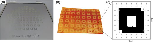
Fig. 2. Patterns used for photolithograpy. (a) Glass mask. (b) Polyimide film with the patterns. (c) Schema of the substrate pattern. The via structures are located on the four sides of a chip, and the center area is located to reinforce the bonded area.
Download figure:
Standard image High-resolution image
Fig. 3. CNT bumps transferred into via holes.
Download figure:
Standard image High-resolution image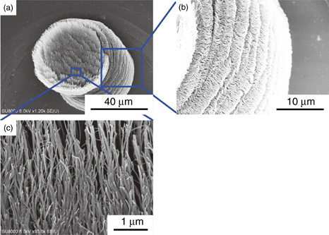
Fig. 4. Top-view SEM images of a VACNT bump via transferred into a via hole. (a) The VACNT bump is fitted into the via hole. (b) The side of the VACNT bump indicates multiple collective bucklings in one lateral direction with the bonding load. (c) The top of the transferred VACNT bump is bristled because of the root of the grown VACNTs.
Download figure:
Standard image High-resolution imageSubsequently, the Si substrate is stripped from the polyimide substrate, leaving VACNT bumps on the polyimide substrate [Fig. 1(5)]. Then, Au is sputtered once again from the stripped side [Fig. 1(6)]. The substrate with VACNT bumps is bonded to the second polyimide substrate with a Au layer on the entire surface, stacking VACNT bumps into via holes completely, which is the second bonding process [Figs. 1(7) and 1(8)]. Furthermore, the first polyimide substrate is etched to expose the top of VACNT bumps [Fig. 1(9)]. Finally, the planed surface is bonded to a circuit substrate (the third bonding process) to finish the fabrication process [Figs. 1(10) and 1(11)]. In this process, both the surfaces of polyimide substrates and VACNT bumps are coincidentally sputter-deposited with Au bumps; therefore, via structures and circuit substrates are shorted. In practice, in the sputtering process, VACNT bumps and polyimide circuit substrates are patterned with a resist to separate the conductive and insulated parts. In this prototype experiment, we followed the fabrication process of flexible multilayer substrates. Therefore, the electrical circuits of these flexible multilayer substrates are designed as follows.
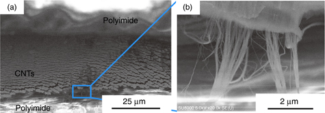
Fig. 5. (a) Cross-sectional image of VACNTs between polyimide substrates. (b) Magnified view of the bonded area of VACNTs and polyimide surface. These views are parts of the center area of the chip shown in Fig. 2(c).
Download figure:
Standard image High-resolution image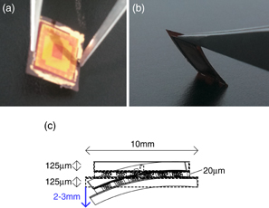
Fig. 6. (a) Bonded flexible substrate images. (b) The bonded substrates can be bent with a pair of tweezers about 2–3 mm from their initial position. (c) The schema of the bent substrates shows tolerance corresponding to an 18–25 mm curvature.
Download figure:
Standard image High-resolution image
2.1. Polyimide etching
Via holes are formed on polyimide substrates for filling VACNTs. First, the trench structure is prepared by dry etching, and then the via hole structure is prepared by wet etching for the back side of the bonded polyimide substrate, as shown in Fig. 1(9).
The patterns shown in Fig. 2 are transferred to polyimide films. The mask is laid with patterns containing bumps with diameters of 50, 100, 150, 200, and 250 µm. A positive photoresist is applied to the surface of a polyimide film and the film with the mask on the surface is exposed to UV light, and the patterns are developed using a photoresist developer. In the etching process, an Ar-ion beam etching machine is used for forming trenches for via structures on a polyimide film at an Ar pressure of 0.02 Pa for 30 min.
Via holes are formed on polyimide substrates for filling VACNTs by photolithography and wet etching. In this procedure, first, a dry film (DF) resist containing Cu metal, which strongly prevents polyimide from being eroded by a developer, is coated on the surface of a polyimide film. Then, the film is exposed to UV light for 5 min and developed similarly to the process of dry etching. After that, the polyimide film is etched away by polyimide etchant before the DF resist is removed.
The fabricated via holes are shown in Fig. 3. Wet etching is markedly faster than dry etching. The diameters of the fabricated via holes at the top and bottom are 200 and 180 µm, respectively, when using a 150-µm-diameter via mask.
2.2. Au magnetron sputtering on top of VACNT bumps
When electrons pass through a CNT, they transport through only one surface layer even through an MWNT. Additionally, caps on the tips of CNTs restrict electrons passing through the inner layers of CNTs.18–20) To increase the electron path through CNTs, some defects are induced on CNTs by plasma or ion beams. Although these defects might cause the degradation of the electronic properties of CNTs,21–23) inner layers of CNTs are uncovered by defects and each inner layer can be connected to electrodes.24) The authors have reported that the defect induction and metal deposition reduce the contact and CNT resistances through Ar-plasma magnetron sputtering.15) When top of VACNTs is sputter-coated with a nominally Au film, Au encapsulates the nanotubes individually instead of forming a uniform Au layer on top of the VACNTs. In addition, the sputtered metals are deposited not only on the surfaces of CNTs but also inside the CNTs.
2.3. Bonding process
The bonding process is required three times in the process of fabricating VACNT vias. Since the first bonding requires the transfer of only VACNT bumps and the accuracy of fitting bumps into via holes, and the second bonding requires the complete stacking of VACNT bumps into via holes, the bonding load is controlled to compress VACNT bumps.25) Such bonding conditions are shown in Table I. Moreover, plasma activated bonding is employed.26–28)
Table I. Bonding conditions of polyimide substrates in the fabrication of flexible multilayer substrates by SAB. The SAB process is performed using Ar plasma.
| Atmosphere for bonding | Air |
| Temperature of bonding stage (°C) | 300 |
| Contact pressure (MPa) | |
| 1st bonding | 0.36 |
| 2nd bonding | 1.2 |
| 3rd bonding | 1.2 |
| Load time (min) | 3 |
| Ar-plasma power (W) | 100 |
| Ar-plasma process time (s) | 30 |
The first bonding has been successfully conducted without a pair of substrates adhering to each other. The VACNT bumps that were transferred into via holes are shown in the scanning electron microscope (SEM) images in Fig. 4. Herein, the VACNT bumps originally grown from a catalyst layer patterned to be 50 µm in diameter are compressed from 100 to 25 µm in height. A higher filling content of CNTs in via holes could be reached by bonding with an applied load. Moreover, SEM images of the VACNT bump with a diameter of 50 µm are shown in Fig. 4. Compared with Fig. 3, the VACNT bump tilts slightly in Fig. 4. The magnified images of the side wall and top of the VACNT bump are shown in Figs. 4(b) and 4(c), respectively. Figure 4(b) indicates multiple collective bucklings in one lateral direction with the bonding load. In Fig. 4(c), the top of the transferred VACNT bump shows bristled VACNTs because of the root of the grown VACNTs. All CNTs in that part do not tangle with each other even after the transfer process.
In the next step, after sputtering Au on the surface, the polyimide substrate with the VACNT bumps through the via holes is bonded to another polyimide substrate with a Au thin layer, completely fitting the VACNT bumps into via holes with a depth of 20 µm. Cross-sectional SEM observation was attempted for the fitted VACNT bump by cutting substrates with scissors. The cutting line was near the center of the chip shown in Fig. 2(c), containing a large area of VACNTs. Then, the cross-sectional surface including VACNTs was exposed by polyimide etching. Figure 5(a) shows that a VACNT via exists between polyimide substrates. Furthermore, in Fig. 5(b), it is confirmed that the VACNTs are bonded to the polyimide surface directly.
3. Results and discussion
The fabricated polyimide/CNT bump multilayer substrate is shown in Fig. 6(a). This bonded substrate consists of 3 polyimide substrates; the VACNT bump via structures are located in the middle polyimide substrate. This substrate can be bent with a pair of tweezers, as shown in Fig. 6(b). Figure 6(c) shows a schema of the bent substrate, indicating that the substrates were bent about 2–3 mm from their initial position, which is equivalent to a tolerance with a curvature of 18–25 mm. However, the bonded substrates are too thick to bend further.
4. Conclusions
In this research, we succeeded in fabricating hybrid structure substrates with VACNTs and polyimide by SAB. Therefore, this fabrication process of flexible multilayer substrates using VACNTs is compatible with semiconductor technologies, with no necessity to lower the CNT growth temperature. Each of the multilayer substrates fabricated in this study consists of a polyimide substrate with a thickness of 125 µm (VACNT layer is 20 µm thick), as a result of overcoming the difficulty in the handling process. Alternatively, the flexibility of the multilayer substrates is relatively sacrificed. It is expected that flexibility will be increased by using thinner substrates (less than 10 µm thickness). Furthermore, this flexible integration technology for high-density integration substrates is expected to be applied to flexible devices, such as ultralight and wearable devices.