Abstract
We demonstrate the synthesis of diamond-like carbon (DLC) doped with highly π-conjugated molecules by codepositing organic semiconductor molecules during the plasma-assisted chemical vapor deposition of DLC. From the results of optical absorption spectroscopy, it was revealed that organic semiconductor molecules reacted with plasma but were not completely decomposed. The results of Raman spectroscopy strongly suggested that a certain chemical moiety remained in the film.
Export citation and abstract BibTeX RIS
1. Introduction
The development of plasma processes for carbon-containing molecules are promising new routes for the production of new carbon materials, since solid-state carbon materials generally have very high melting temperature and do not dissolve in solvents. It is expected that this research direction will lead to a new field of chemistry for synthesizing carbon-based materials with novel and useful physical properties. Examples can be found in the plasma synthesis of diamondoid,1–3) the doping of carbon solid with various elements,4–7) and the facile synthesis of single wall carbon nanotubes.8,9)
Diamond-like carbon (DLC) is widely used in various applications such as hard coatings, gas barriers, and anticorrosion coatings.10,11) DLC is produced by the plasma deposition of carbon and hydrogen using hydrocarbon gases as the source materials. Because of its simple coating process and wide application, DLC is now produced on a large industrial scale. However, the microscopic structures of DLC have been characterized only recently, and precise control of the nanostructures in DLC has not yet been established. The nanostructure control of carbon in DLC will lead to various useful properties such as tribology,12–14) controlled refractive index10,15,16) and other optical properties,10,15,16) electronic and electrochemical properties,5,6,17–19) catalytic activities,20–22) and biological functions.23,24) Although there are various distinctions among sp3-rich carbon–hydrogen systems,11) we use the term "DLC" in this paper for simplicity.
We are studying the fabrication of nanostructured carbon materials using plasma processing. Our interest is in the reaction of extended π-electron systems of organic semiconductor molecules with plasma, which is a kind of interaction between plasma and nanointerfaces.25) In this paper, we report the codeposition of large organic molecules during the fabrication of DLC by plasma CVD. The molecules used were copper phthalocyanine (CuPc, C32H16N8Cu) and perylenetetracarboxylicdianhydride (PTCDA, C24H8O6), both of which are known as robust dye molecules and have recently attracted attention as organic semiconductors. Optical properties and Raman spectra were examined for the characterization of the resulting materials.
2. Experiments
We used a rather unique arrangement for the plasma deposition of DLC to confine the plasma and allow for large organic molecules to be incorporated in the DLC without excessive decomposition. A schematic drawing of the deposition chamber is shown in Fig. 1 . The chamber is equipped with the plasma source (an RF-sputter gun), a molecular source (a Knudsen-cell), a gas inlet, and a pumping line with a bypass valve. The sample holder is made of stainless steel and is floated at −400 V from the ground level in order to deposit sp3-carbon-rich DLC. After the introduction of the substrate [Al2O3(0001) with dimensions of 5 × 5 × 0.43 mm3] and molecular source, the chamber was pumped down to 10−4 Pa by a turbo molecular pump (TMP), and then the pumping rate was reduced by closing the main valve. Methane gas, the carbon and hydrogen source, was supplied from a needle valve. The pumping rate was controlled to adjust the pressure of CH4 to 10 Pa. The sample bias (−400 V) was then applied and the plasma was ignited. The plasma was produced using a 1 inch RF sputtering gun with a graphitic carbon target. The size of the white glow of the plasma is about 5 cm, and it did not directly touch the substrate or the molecular source, as observed visually. After the stabilization of the RF plasma, the molecular source was heated to a certain temperature (∼250 °C for CuPc and ∼200 °C for PTCDA, which is intended to dope these molecules by ∼10% into DLC). The temperature of the substrate was not controlled. It was found that the temperature during the deposition did not exceed 60 °C.
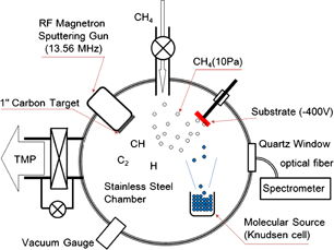
Fig. 1. Schematic drawing of the plasma-CVD chamber equipped with the molecular source. The plasma was produced by an RF magnetron sputtering gun with a graphitic carbon target. The sputtering gun was set not facing the substrate to avoid direct deposition of sputtered carbon. CH4 was supplied as the atmospheric gas and additional C and H source. Organic semiconductor molecules were evaporated from a Knudsen cell facing the substrate.
Download figure:
Standard image High-resolution imageThe optical emission spectra during the DLC deposition were measured using a fiber coupled spectrometer (Ocean Optics USB2000). The optical absorption spectra and Raman spectra of the films were obtained using Lambda 900 (Lambda Physics) and InVia (Renishaw, 20×–50× objective lens and 532 or 785 nm excitation), respectively.
3. Results and discussion
Figure 2
shows the optical emission spectra (OES) profiles during the deposition. The main emissive components are Hα (657 nm), Hβ (486 nm), and CH (A2Δ → X2Π at 430.6 and 430.7 nm, → X2Π at 390.3 nm),26–28) which consistute the typical C–H plasma for the deposition of DLC. Because the emission from C2 (516 nm) is very weak, the chemistry in the plasma is governed by hydrogen-containing species. The OES profiles did not change noticeably by the codeposition of the organic semiconductor molecules, which means that the concentration of the organic semiconductor molecules was low. This suggests that the organic semiconductor molecules did not react with each other. The C- and H-containing radicals in the plasma mainly interacted with them. This is not always the case, however, owing to the high backpressure of CH4 (10 Pa), which might cause clustering during the deposition. This issue will be discussed later.
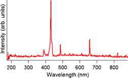
Fig. 2. Optical emission spectrum during the deposition of DLC using the present setup. The spectrum for co-evaporation of CuPc or PTCDA was almost identical to the spectrum in this figure.
Download figure:
Standard image High-resolution imageIn the following, we describe the results of CuPc first, and then those of PTCDA. Figure 3 shows the optical absorption spectra of (a) a DLC film, (b) a DLC with a codeposited CuPc film, and (c) a pristine CuPc film. The DLC (a) shows a very smooth increase in the optical absorption starting from 500 nm. This reflects the amorphous nature of DLC. DLC "doped- with" CuPc (b) shows absorption at 350 nm and a broad peak centered at 630 nm. In the case of the pristine CuPc film (c), a Soret band (∼350 nm) and a Q-band (550–750 nm) with substantial Davydov splitting are observed as reported.29) The resemblance in the optical absorption between (b) and (c) suggests that the CuPc molecules were not decomposed completely. Because the Davydov splitting comes from the interaction between transition dipoles with fixed geometry in crystalline solids, the CuPc molecule separately embedded in the matrix (DLC in the present case) will show a single peak in the optical absorption. The less pronounced splitting of Q-band absorption in (b) might come from this isolation effect or the destruction of the molecule.

Fig. 3. Optical absorption spectra of (a) DLC film, (b) DLC with codeposited CuPc film, and (c) pristine CuPc film. The splitting in (c) comes from the Davydov splitting, which is caused by the interaction between optically excited molecules.
Download figure:
Standard image High-resolution imageTo examine the above possibilities, we measured the Raman spectra of the samples. Figure 4 shows the Raman spectra of (a) the DLC codeposited with CuPc, (b) the CuPc single crystal, and (c) the pristine CuPc film fabricated by vacuum deposition. A broad peak from 1000 to 1800 cm−1 is typically observed in DLC. The center of this peak is at approximately 1390 cm−1, which indicates the formation of almost full sp3 DLC (below 1400 cm−1). Note that the Raman spectra depend on the crystal structure of CuPc, that is of the β-type in (b) and mainly of the α-type in (c).30) By comparing the spectra shown in Fig. 4(a) and with those in Figs. 4(b) and 4(c), we can observe that the molecular fingerprint of the Raman spectra is surprisingly maintained as marked by the arrows, although the peaks broadened and somewhat shifted. We consider that the vibrational structure of the extended π-conjugate molecule is almost intact, which means that only minor changes occur in the structure, such as the replacement of peripheral hydrogen by CH3 carbon. However, the CuPc molecules definitely reacted with plasma to form some new chemical bonds, because the broadening and shift of the Raman peaks were observed and many Raman peaks disappeared. The small splitting of the optical absorption Q-band [Fig. 3(b)] may also be explained by this covalent bond formation, without considering the clustering of CuPc in the vapor phase.

Fig. 4. Raman spectra of (a) DLC codeposited with CuPc, (b) CuPc single crystal, and (c) pristine CuPc film fabricated by vacuum deposition. "s" in (a) denotes the signal from the substrate. The difference between (b) and (c) comes from the difference in the polytype of CuPc crystals.
Download figure:
Standard image High-resolution imageFigure 5 shows the optical absorption spectra of (a) DLC [same as in Fig. 3(a)], (b) the DLC codeposited with PTCDA, and (c) the pristine PTCDA film. Because the spectrum change between (b) and (c) is substantial, we consider that the π-electron system of PTCDA was substantially altered, which led us to infer that the PTCDA molecules have been decomposed with the C–H plasma. Figure 6 shows the Raman spectra of (a) the DLC co-deposited with PTCDA and (b) the pristine PTCDA film. The shape of the DLC region from 1000 to 1800 cm−1 shows that the DLC is again mainly of the sp3-type, but that the sp2/sp3 ratio is increased from that in the case of the CuPc-doped DLC, because the peak shifted to higher wave numbers. The striking difference from CuPc is that only one distinct peak different from DLC is found in (a), at approximately 1080 nm. There is a strong peak near this wave number in the pristine PTCDA. This peak has been assigned by quantum chemical computation to the in-plane C–O–C bending.31) Our experimental result strongly suggests that this moiety (C–O–C) was robust and did not decompose during the interaction with C–H plasma. Combined with the upshift of the DLC peak, we consider that the decomposed π-electron systems of PTCDA by C–H plasma contribute to the increased sp2/sp3 ratio.
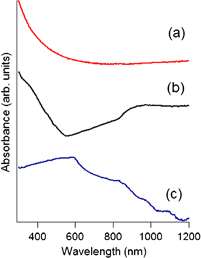
Fig. 5. Optical absorption spectra of (a) DLC [same as in Fig.3(a)], (b) DLC codeposited with PTCDA, and (c) pristine PTCDA film.
Download figure:
Standard image High-resolution image
Fig. 6. Raman spectra of (a) DLC codeposited with PTCDA and (b) pristine PTCDA film. The peak at 1080 cm−1 in (a) is considered to be of the same origin as the peak at 1060 cm−1 in (b), which is identified as C–O–C vibration. The peak at 420 cm−1 in (a) is the signal from the substrate.
Download figure:
Standard image High-resolution image
4. Conclusions
We fabricated novel carbon films by codepositing large organic semiconductor molecules during the plasma-assisted chemical vapor deposition of DLC, which can be regarded as an attempt at doping molecules with extended π-systems into DLC. The OES result shows that C–H radical plasma was formed in the process, even with the codeposition of π-electron molecules. The DLC was composed of mostly sp3 as examined by Raman spectroscopy; however, the sp2/sp3 ratio was slightly dependent on the type of dopant molecules. In the case of CuPc, the doped film showed a similar optical absorption profile to the pristine molecular film, but substantially different Raman spectra were observed. PTCDA showed a substantial destruction of the π-electron system from the optical absorption and Raman spectroscopy results. The Raman spectrum of PTCDA-doped DLC indicated that the carboxylic dianhydride (C–O–C) moiety remains intact during the plasma process. The sp2/sp3 ratio slightly increased in the case of PTCDA, which might have been caused by the decomposed π-electron species.
Acknowledgments
This work was supported in part by a Grant-in-Aid for Scientific Research on Innovative Areas "Frontier Science of Interactions between Plasmas and Nano-Interfaces" (Grant No. 21110002) from the Ministry of Education, Culture, Sports, Science and Technology of Japan (MEXT). We would like to thank Professor T. Hasegawa (The University of Tokyo) for valuable discussions and support through the JST-CREST program. The experimental work was conducted at Hokkaido University, supported by the "Nanotechnology Platform" Program of MEXT.
Biographies

Wei Xie obtained B. Eng. and M. Eng. from Sichuan University, China. He is a Ph. D. course student at Graduate School of Chemical Science and Engineering (CSE), Hokkaido University since 2012.

Naoki Muraya graduated Hokkaido University in 2011. He is now a graduate student at CSE, Hokkaido University.

Takashi Yanase graduated Osaka University. He obtained Dr.Sc. from The University of Tokyo in 2011 and currently works as a project assistant professor at Frontier Science Center, Hokkaido University.

Taro Nagahama obtained B.Sc., M.Sc., and Dr.Sc. degrees from Kyoto University. He worked at National Institute of Advanced Industrial Science and Technology (AIST) as a staff scientist. He is associate professor of Faculty of Engineering, Hokkaido University since 2011. His main research field is spintronics.

Toshihiro Shimada obtained B.Sc., M.Sc., and Dr.Sc. degrees from The University of Tokyo. He worked there as research associate, lecturer and associate professor. He moved to Hokkaido University in 2010 as professor at Division of Materials Chemistry. His current interest is solid state chemistry and thin film technology, especially by high energy processes.