
Abstract
Ga2O3 film growth on InGaAs substrates was investigated using an atomic layer deposition system with trimethylgallium (TMGa) and H2O as precursors. Self-limiting growth of Ga2O3 was confirmed on InGaAs substrates as well as on Si and GaAs. During initial formation of the Ga2O3 film on an InGaAs substrate, the selective self-cleaning effect of TMGa on AsOx and GaOx was observed. The insertion of ultrathin Ga2O3 into an Al2O3/InGaAs gate stack as an interfacial passivation layer proved quite effective to reduce Dit around the midgap. The Al2O3/InGaAs MISFET performance also revealed improvement of the effective mobility for both NH4OH- and (NH4)2S-treated devices.
Export citation and abstract BibTeX RIS
The passivation of high-k/III–V interfaces has long been investigated with the aim for realizing superior channel quality for next-generation metal–insulator–semiconductor field-effect transistor (MISFET) applications. The most important challenge is engineering the interface between the channel material and gate dielectrics. The native oxide of III–V MIS generate defects in the form of As–As bonding and Ga dangling bonds, which causes a high interface trap density (Dit), and introduces strong Fermi-level pinning and severe deterioration of channel mobility.1,2) Therefore, several oxide removal techniques such as aqueous HCl and NH4OH etching,3) sulfur passivation,4–6) selenium passivation,7) self-cleaning with Al(CH3)3 (trimethylaluminum; TMA),8–12) and H2 plasma cleaning,13) have been reported for the improvement of the GaAs and InGaAs channel properties. In addition to oxide removal, further surface passivation techniques such as plasma nitridation14,15) and epitaxial Si passivation16) have been proposed to control the anion composition at the MIS interface.
Although there have been many reports that removal of the Ga oxide component correlate with improvements in the MIS properties, some reports showed that Ga2O was observed after TMA cleaning and Si passivation,17,18) and an InGaAs MISFET with molecular beam epitaxy (MBE)-grown Al2O3/Ga2O3(Gd2O3) stacked gate dielectric exhibited superior characteristics.19) Therefore, the effects of GaOx species at III–V MIS interfaces are under debate at present. A scanning tunneling microscopy (STM) study showed that Ga2O formation on InGaAs by MBE started with Ga2O molecules bonding to As atoms, and disordered structures were formed after full coverage.20) Another group also reported that Ga2O did not passivate nor unpin the interface and was unable to form on the InGaAs surface. The capacitance–voltage (C–V) characteristics of Al2O3/InGaAs with Ga2O passivation also exhibited large frequency dispersion, which indicates high Dit and Fermi level pinning.21) On the other hand, Ga2O film passivation on GaAs using the MBE technique has also been demonstrated.22,23) A monolayer of Ga2O formed a crystalline interface that was electronically unpinned due to Ga2O restoring the surface As and Ga atoms to near-bulk charge.23)
The deposition technique to obtain GaOx film should also be considered. Many deposition methods for GaOx film growth have been successful, including MBE,20–23) atomic layer deposition (ALD),24) plasma-enhanced ALD (PEALD),25) and electron beam evaporation.26) Among these techniques, ALD has received significant interest due to its intrinsic self-terminated growth nature.27) Although ALD of GaOx films using Ga(CH3)3 (trimethylgallium; TMGa) and H2O is known to be difficult due to the high decomposition temperature of TMGa (ca. 300 °C),28,29) it has an advantage to form a thin passivation layer at the MIS interface from the viewpoint of equivalent oxide thickness (EOT) scaling. In this paper, we report that an ultrathin Ga2O3 layer can be grown in a self-limiting manner by utilizing the ALD chemistry of TMGa and H2O. The impact of Ga2O3 layer insertion to the Al2O3/InGaAs interface on the MIS structure is also investigated.
Experiments were conducted using an ALD system with TMA, TMGa, and H2O as precursors. In0.53Ga0.47As(001) samples employed for this study were epitaxial wafers prepared by metal organic chemical vapor deposition (MOCVD) on InP wafers. MIS capacitors and MISFETs were fabricated on n-type Si-doped and p-type Zn-doped InGaAs epitaxial layers, respectively. The thickness and doping concentration of the epitaxial layer were 0.5 µm and ca. 3 × 1016 cm−3, respectively, both for the n- and p-type InGaAs. To fabricate a capacitor, n-InGaAs(100) substrates were treated in NH4OH solution for 1 min and rinsed in deionized (DI) water for 1 min prior to ALD. ALD of a 10-nm-thick Al2O3 layer was performed using a fixed deposition temperature of 250 °C and at a rate of 0.1 nm/cycle. Postdeposition annealing (PDA) was conducted in vacuum at 400 °C for 2 min. After gate electrode and back contact evaporation, postmetallization annealing (PMA) was performed in Ar at 350 °C for 2 min.
Figure 1 shows the change in the GaOx film thickness on n-Si(001), n-GaAs(001), p- and n-InGaAs(001) substrates with the number of deposition cycles up to 150. All the III–V surfaces were prepared by NH4OH treatment, and the Si surfaces were untreated prior to GaOx deposition. The oxide thicknesses were measured and normalized using spectroscopic ellipsometry according to the reference refractive-index data for Ga2O3 and the Cauchy model. GaOx growth was conducted by repeating the cycle of TMGa and H2O supply at 250 °C. The TMGa dosage was set at 500 Pa·s, which was much higher than the TMA dosage for Al2O3 growth (ca. 1 Pa·s), to ensure the sufficient TMGa supply. GaOx growth on the GaAs substrates could be detected after the deposition of more than 30 cycles, at which time the GaOx film thickness became saturated at ca. 0.2 nm. GaOx growth on the InGaAs substrates was similar to that on the GaAs substrates. Although GaOx growth on the Si substrates was detected instantly after the first cycle, the thickness became saturated at ca. 1 nm. These results indicate that a thick GaOx film cannot be formed using the deposition chemistry of TMGa and H2O. However, monolayer GaOx film can be grown on GaAs and InGaAs substrates in the manner of self-limiting growth after the initial incubation period. The difference in the initial formation of GaOx on Si and GaAs substrates implies that the self-cleaning on the III–V surface by TMGa was carried out similarly to that for TMA.11) In addition, the thickness difference in the GaOx film on native SiO2 and GaAs substrates may be slightly distorted because the thickness was calculated using the same refractive index.

Fig. 1. Normalized GaOx film thickness prepared with various deposition cycles at a substrate temperature of 250 °C.
Download figure:
Standard image High-resolution imageTo reveal the growth of the self-limiting GaOx film, X-ray photoelectron spectroscopy (XPS) scans were obtained with and without GaOx film. Figures 2(a) and 2(b) show As 2p3/2 and Ga 2p3/2 XPS spectra of the NH4OH-treated n-InGaAs(001) surface and that following the deposition of ALD-Al2O3 (1 nm) and ALD-GaOx (30 cycles)/ALD-Al2O3 (1 nm). In this experiment, all the samples were analyzed using ex situ XPS with an Al Kα X-ray source (1,486.7 eV). Figure 2(a) shows that the oxides on the InGaAs surface were effectively reduced by 1 nm Al2O3 capping due to the self-cleaning effect of TMA.10,11) The As 2p peak was also reduced by insertion of the GaOx layer. This behavior indicated that TMGa also has a self-cleaning effect analogous with TMA. On the other hand, the Ga 2p spectra in Fig. 2(b) after Al2O3 and GaOx/Al2O3 depositions presented a contrastive characteristic. NH4OH treatment left a surface oxide that exhibited a large shoulder on the high-binding-energy side of the bulk peak at 1.6 eV, which was possibly due to Ga(AsO3)3 or Ga(OH)3.17) While direct Al2O3 deposition reduced the GaOx layer, ALD-GaOx treatment realized distinct GaOx growth on the InGaAs surface with chemical shift of 1.2 eV corresponding to Ga3+ oxidation state.9) The chemical shift reduction from 1.6 to 1.2 eV indicates the removal of the higher oxidation component of Ga and the formation of the interfacial Ga2O3 layer between Al2O3 and InGaAs. The increase in thickness of the Ga2O3 layer by inserting the ALD-GaOx was estimated from the Ga 2p peak to be 0.11 nm, which is consistent with the ellipsometry result shown in Fig. 1. These results indicate that TMGa had a selective self-cleaning effect on unnecessary AsOx and GaOx, similar to TMA, as well as significantly contributes to the formation of Ga2O3. Both Figs. 1 and 2 indicate monolayer termination on the InGaAs surface by ALD-Ga2O3 growth, which was eventually suitable to be an ultrathin passivation layer.
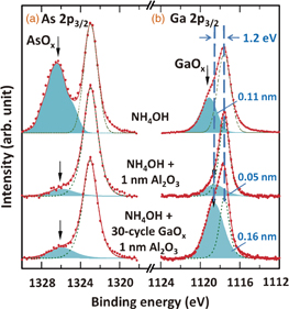
Fig. 2. (a) As 2p3/2 and (b) Ga 2p3/2 XPS spectra of NH4OH-treated n-InGaAs(001) surfaces with deposition of ALD-Al2O3 (1 nm) and ALD-Al2O3 (1 nm)/30-cycle ALD-GaOx. Al Kα (1,486.7 eV) was used as an X-ray source.
Download figure:
Standard image High-resolution imageA possible mechanism for Ga2O3 formation on InGaAs can be described as follows. AsOx and GaOx on the InGaAs surface are first reduced by the self-cleaning effect with exposure to TMGa, as shown in Fig. 2(a), and the surface is partially covered with Ga(CH3)n molecules (where n = 1 or 2). This selective absorption is limited by the bonding requirements and steric effects,29) and no Ga(CH3)n molecules are absorbed on Ga atoms at the surface.30) After surface oxide removal processing, (CH3)n is desorbed after the supply of H2O and is decomposed into Ga-OH29,31) or Ga2O3, as shown in Fig. 2(b). Repeated cycling of alternate TMGa and H2O supply then provides almost complete surface coverage with Ga-OH because decomposition is difficult at low temperature. Ga(CH3)n molecules are rarely absorbed on this surface, so that Ga2O3 formation becomes more difficult. Therefore, the self-limiting growth of monolayer Ga2O3 on the InGaAs surface is achieved. This monolayer (1 ML) Ga2O3 layer could be chemically stable, with the potential to provide a low interface trap density (Dit) and prevent the intermixing of InAlGaAs at the MIS Al2O3/InGaAs interface.
Figures 3(a) and 3(b) show the C–V characteristics and conductance data for the (1) ALD-Al2O3 (10 nm)/InGaAs and (2) ALD-Al2O3 (10 nm)/30-cycle ALD-Ga2O3/InGaAs MIS capacitors (MISCAPs) with Au electrodes. The sample with the Ga2O3 passivation layer showed a reduction of capacitance under negative bias. Frequency dispersions around the flatband voltage (Vfb) and under charge accumulation were also slightly affected by the Ga2O3 passivation layer compared with the control sample, as shown in Figs. 3(a-1) and 3(a-2). A significant effect of Ga2O3 passivation was observed in the conductance data obtained at room temperature. The conductance at low frequencies was significantly reduced by the Ga2O3 passivation layer and the difference in the conductance peaks was clearly evident from a comparison of Figs. 3(b-1) and 3(b-2). The decrease in conductance may be caused by a reduction of the border trap in the Al2O3 film near the MIS interface by Ga2O3 passivation.32) Dit profiles for both the sample with the Ga2O3 passivation layer and the control sample from a bias voltage of Vfb = 0 to −0.5 V are shown in Fig. 4 . Dit was estimated using the conductance method assuming that Dit = 2.5/q × Gp/ω. Dit around the midgap of the InGaAs bandgap was extensively reduced over a wide range by Ga2O3 passivation. A minimum Dit as low as 2.4 × 1011 cm−2 eV−1 was achieved.

Fig. 3. (a) C–V characteristics and (b) conductance at room temperature for (1) ALD-Al2O3 (10 nm)/InGaAs and (2) ALD-Al2O3 (10 nm)/30-cycle ALD-Ga2O3/InGaAs capacitors with Au electrodes.
Download figure:
Standard image High-resolution image
Fig. 4. Interface trap densities of the ALD-Al2O3 (10 nm) InGaAs structure with and without a 30-cycle ALD-Ga2O3 passivation layer.
Download figure:
Standard image High-resolution imageTo investigate the impact of Ga2O3 passivation on MISFET performance, n-channel InGaAs MISFETs were fabricated using the Ni-alloy process with and without Ga2O3 passivation of NH4OH- or (NH4)2S-treated surfaces. The p-InGaAs surface was first prepared by wet etching for 1 min in NH4OH or 5 min in (NH4)2S and rinsed with deionized water for 1 min. Deposition of the Al2O3 gate dielectric layer with and without a 30-cycle Ga2O3 passivation layer was then performed. PDA was performed at 400 °C for 2 min. A 30-nm-thick TaNx gate electrode was then deposited on the Al2O3 film by sputtering. TaNx and Al2O3 gate were selectively removed by sulfur hexafluoride (SF6) reactive ion etching and buffered hydrofluoric (BHF) wet etching, respectively. A 25-nm-thick Ni electrode layer was deposited by electron beam evaporation and annealed in Ar at 350 °C for 2 min. Finally, the fabrication process was completed by the etching of the unreacted Ni in HCl : DI water (1 : 5) for source, drain, and gate electrode isolation.
Figures 5 (a-1) and 5(a-2) show the drain current–gate voltage (ID–VG) characteristics of the NH4OH- and (NH4)2S-treated Al2O3/InGaAs MISFETs, respectively. ID–VG curves with and without Ga2O3 passivation layers of 100-µm-gate-length devices were measured at drain voltages (VD) of 50 mV and 1 V. The subthreshold slopes (SS) were 236 and 147 mV/decade for the NH4OH- and (NH4)2S-treated control devices, which were improved to 198 and 141 mV/decade after Ga2O3 passivation, respectively. The threshold voltages (Vth) were not significantly changed after passivation with the Ga2O3 layer for the NH4OH- and (NH4)2S-treated devices. The on/off ratios were improved for both treatments by Ga2O3 passivation. Lower off-currents were achieved with Ga2O3 passivation due to the reduction of surface leakage current. Although the SS values were reduced by Ga2O3 passivation, further improvement could be achieved by controlling the junction quality and channel metal connection.

Fig. 5. (a) Id–Vg and (b) μeff for (1) NH4OH- and (2) (NH4)2S-treated Al2O3/InGaAs n-channel MISFETs with and without a 30-cycle ALD-Ga2O3 passivation layer.
Download figure:
Standard image High-resolution image
Figures 5(b-1) and 5(b-2) show the effective mobility (μeff) as a function of the inversion carrier density (Ns) for the NH4OH- and (NH4)2S-treated devices, respectively. The Ns value was estimated by the split C–V method at 10 kHz. μeff for the Ga2O3 passivation devices were significantly higher than that for the control devices with both treatments over the entire Ns range. μeff for the NH4OH- and (NH4)2S-treated devices with Ga2O3 passivation were increased by around 2.3 and 1.5 times that of the control devices, respectively. The improvement in µeff for the NH4OH-treated device by Ga2O3 passivation was associated with MISCAP data. The Ga2O3 passivation layer improved the Al2O3/InGaAs MIS interface properties by reducing the native oxide and terminating Ga2O3 onto the surface. The combination of (NH4)2S treatment and Ga2O3 passivation layer revealed superior improvement of the Al2O3/InGaAs gate stack, which may be due to a reduction of Dit both near the conduction band edge4–6) and around the midgap in the Al2O3/InGaAs MIS structure, respectively.
In conclusion, an ultrathin Ga2O3 interface layer was grown in a self-limiting manner using ALD with TMGa and H2O precursors. Interaction of TMGa and H2O with OH groups possibly restricted the formation of the Ga2O3 film. The self-cleaning effect of TMGa on AsOx at the InGaAs surface was observed, similar to that for TMA. Insertion of the ultrathin Ga2O3 layer to the Al2O3/InGaAs interface was effective to reduce the trap density around the midgap. The MISFET performance characteristics also showed improvement of μeff by ultrathin Ga2O3 passivation for both NH4OH- and (NH4)2S-treated devices. These experimental results demonstrate that Ga2O3 passivation does improve Al2O3/InGaAs MIS interface and FET performance.
Acknowledgements
This study was supported by the Japan Society for the Promotion of Science (JSPS) through the Funding Program for World-Leading Innovative R&D on Science and Technology (FIRST program) initiated by the Council for Science and Technology Policy (CSTP), Cabinet Office, Government of Japan.