

Abstract
Lateral GaN MOSFETs on homoepitaxial p-GaN layers with different Mg doping concentrations ([Mg]) have been evaluated to investigate the impact of [Mg] on MOS channel properties. It is demonstrated that the threshold voltage (Vth) can be controlled by [Mg] along with the theoretical curve. The field effect mobility also shows [Mg] dependence and a maximum field effect mobility of 123 cm2 V−1 s−1 is achieved on [Mg] = 6.5 × 1016 cm−3 layer with Vth = 3.0 V. The obtained results indicate that GaN MOSFETs can be designed on the basis of the doping concentration of the p-GaN layer with promising characteristics for the realization of power MOSFETs.
Export citation and abstract BibTeX RIS
GaN is one of the promising materials for next-generation power conversion systems and attracts much attention owing to its wide-bandgap energy and large critical electric field.1) AlGaN/GaN high-electron-mobility transistors (HEMTs) have been developed extensively so far with a heteroepitaxial GaN layer on a Si substrate from a cost-effective viewpoint and have demonstrated outstanding performance.2–5) However, vertical device structures are more suitable for handling high voltages and large currents even on GaN layers similarly to Si or SiC. With the recent progress of bulk GaN crystal growth,6) an increasing number of demonstrations of vertical structures with breakdown voltages higher than 1 kV have been made on high-quality homoepitaxial GaN layers.7–17)
For high-power switching systems, a MOS-gate structure is preferable from many viewpoints such as gate drive controllability, low power consumption of its drive circuit, and parallel use for high current operation. Most importantly, an enhancement-mode operation is strongly required to prevent a turn-off failure for circuit safety. Thus, it is necessary to design a MOS-gate device with an appropriate threshold voltage (Vth), for example, >3 V.
Some previous works have reported enhancement-mode MOSFETs on p-GaN layers both in the lateral and vertical structures,18–24) but sometimes Vth shows a large deviation from the expected value; thus, a Vth control has not been well established so far on GaN. In principle, Vth should be determined by the capacitance of the gate insulator, the acceptor concentration, and the work function of the gate electrode if the interface state density (Dit) is sufficiently low.25) In addition to the Vth control, a high channel mobility is also important for the realization of low-on-resistance MOSFET devices, because the channel resistance could dominate the total resistance in the case of GaN owing to the material capability of a quite low drift layer resistance. A channel mobility of more than 100 cm2 V−1 s−1 must be achieved in order to realize vertical MOSFETs with specific on-resistance (RonA) < 1 mΩ cm2 for over 1 kV devices.22) From these requirements, a systematical investigation about MOS channel properties is needed in controlled p-GaN layer and high-quality MOS interface systems. In this letter, we present the inversion channel lateral MOSFETs fabricated on homoepitaxial p-GaN layers and demonstrate the control of MOS channel properties such as Vth and channel mobility by changing the Mg doping concentration in the p-GaN layer.
Lateral MOSFETs were fabricated on homoepitaxial p-GaN layers grown by MOCVD on freestanding n-type GaN(0001) substrates obtained by HVPE growth. The Mg doping concentrations ([Mg]) in the p-GaN layers were 4.9 × 10¹⁷, 1.4 × 10¹⁷, and 6.5 × 1016 cm−3, which were analyzed by SIMS measurements. We performed post-growth annealing at 650 °C for 30 min in oxygen atmosphere to activate Mg as an acceptor. Here, we confirmed that the homoepitaxially grown Mg-doped layers with these doping concentrations and post-growth annealing have exhibited p-type characteristics with low-compensation donors.26) Figure 1 shows a schematic cross section of the fabricated lateral GaN MOSFETs. The source and drain regions were selectively formed by Si ion implantation followed by activation annealing at 1100 °C. After activation annealing, we deposited a SiO2 film at 300 °C by using a plasma-CVD apparatus with tetraethyl orthosilicate (TEOS) gas as a Si source. The typical refractive index range is from 1.46 to 1.47, which is close to that of a thermal oxide. The equivalent oxide thicknesses determined by capacitance–voltage (C–V) measurement under the accumulation condition of the SiO2/n-GaN test element structure on the fabricated MOSFET wafers were 126, 111, and 115 nm for [Mg] = 4.9 × 10¹⁷, 1.4 × 10¹⁷, and 6.5 × 1016 cm−3 samples, respectively. Aluminum metal was used as a gate metal and also as a source and drain contact metal to simplify the fabrication process. Forming gas annealing was performed after Al patterning at 400 °C for 30 min.
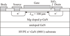
Fig. 1. Schematic cross section of the fabricated lateral GaN MOSFETs.
Download figure:
Standard image High-resolution imageHere, we confirmed the SiO2/GaN interface quality by using an n-GaN MOS capacitor. Figure 2 shows the obtained C–V characteristics of a SiO2/n-GaN MOS capacitor measured in the frequency range between 1 MHz and 300 Hz. The frequency dispersion in the C–V curves is negligible, indicating a low interface trap density Dit. We performed Dit analysis by using the Hi–Lo method and also the conductance method. Both methods show Dit less than 1 × 1011 cm−2 eV−1 at Ec − 0.2 eV, indicating good MOS interface at least near the conduction band edge.

Fig. 2. C–V characteristics of deposited SiO2/n-GaN MOS capacitor. The multiple C–V curves measured in the frequency range of 1 MHz to 300 Hz are plotted together. The dashed line is the calculated ideal curve.
Download figure:
Standard image High-resolution imageIn order to extract the MOS channel behavior, long-channel MOSFETs with a channel length (Lch) of 100 µm and a gate width (Wg) of 100 µm were evaluated. By using long and wide channel patterns, we can ignore the error of channel length and width values from the photomask pattern. Furthermore, it is possible to eliminate the parasitic resistance of the source and drain regions. In fact, the contact and sheet resistances of the source and drain regions monitored using the TLM pattern were 4.8 × 10⁻⁵ Ω cm2 and 190 Ω/sq, respectively, whose contributions were sufficiently low compared with that of the MOS channel resistance from the 100-µm-long channel; thus, the obtained characteristics can be almost attributed to the MOS channel behavior.
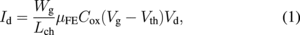
Figure 3 shows the typical Id–Vd output characteristics of the fabricated lateral MOSFETs. Nearly ideal MOS channel behaviors, such as those in a linear region, a nonlinear region, and a saturation region, are clearly observed. The Id–Vg transfer characteristics in the linear region were measured at Vd = 0.1 V. The obtained Id–Vg curves are shown in Fig. 4(a). Vth is determined as a gate bias intercept of the linear extrapolation of Id based on the current equation of the linear region,27)
which corresponds to the strong inversion point. Here, μFE is the field effect mobility and Cox is the gate oxide capacitance. The extracted Vth values were 15.5, 5.2, and 3.0 V on [Mg] = 4.9 × 10¹⁷, 1.4 × 10¹⁷, and 6.5 × 1016 cm−3 layers, respectively. The obtained Vth dependence against Mg doping concentration is quite similar to the calculated dependence as shown in Fig. 4(b). These results indicate that the Vth of GaN MOSFETs can be controlled and designed on the basis of the Mg doping concentration of the p-GaN layer similarly to the case of Si.
Fig. 3. Id–Vd output characteristics of fabricated MOSFET on [Mg] = 1.4 × 1017 cm−3. The measured device has a gate width of 100 µm and a channel length of 100 µm.
Download figure:
Standard image High-resolution image
Download figure:
Standard image High-resolution image
Fig. 4. (a) Id–Vg transfer characteristics in the linear region of fabricated MOSFETs measured at Vd = 0.1 V. The linear extrapolation for Vth determination was made in the maximum gm region. (b) [Mg] dependence of the extracted Vth and the comparison with theoretical behavior calculated with 110- to 130-nm-thick SiO2 gate oxide for the comparison of experimental thickness ranges. For theoretical calculation, 100% Mg activation is assumed.
Download figure:
Standard image High-resolution imageAs seen in Fig. 4(b), the experimental Vth values show negative voltage shifts from the calculated curves, which are −7.2, −5.3, and −4.3 V for [Mg] = 4.9 × 10¹⁷, 1.4 × 10¹⁷, and 6.5 × 1016 cm−3 samples, respectively. One of the causes of these voltage shifts is thought to be the effective charges at the MOS interface. As shown in Fig. 2, we observed a negative flatband voltage shift of −3.3 V in n-GaN MOS capacitors, corresponding to the effective positive charge of 6.2 × 1011 cm−2 at the interface, which is the summation of fixed positive and interface-trapped negative charges. The voltage shifts calculated from these effective charges are −3.6, −3.2, and −3.3 V for [Mg] = 4.9 × 10¹⁷, 1.4 × 10¹⁷, and 6.5 × 1016 cm−3 samples, respectively, by taking the variation in oxide thickness into account. The observed shifts are larger than these expected shifts. The possible explanation for this is the introduction of compensation donors such as nitrogen vacancies during the MOSFET process, which gives the discrepancies between [Mg] and the effective acceptor concentration. We tried to determine the effective acceptor concentration by capacitance measurement on the fabricated MOSFETs, but the high series resistance inhibited the valid measurement because of the poor ohmic contact of Al with p-GaN layers. In addition, it is necessary to confirm the Vth dependence against the SiO2 thickness experimentally in order to distinguish the contribution of fixed positive charges at the interface from that inside the films for a more precise discussion. Further work and process improvements are required to explain these discrepancies.
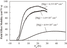
The field effect mobility curves calculated from the Id–Vg characteristics are shown in Fig. 5. The field effect mobility gradually increases with the applied gate voltage and shows a peak at a certain gate voltage. The maximum field effect mobility monotonically increases with decreasing Mg doping concentration, and the peak values are 33.1, 108, and 123 cm2 V−1 s−1 on [Mg] = 4.9 × 10¹⁷, 1.4 × 10¹⁷, and 6.5 × 1016 cm−3 layers, respectively. The channel mobility is known to be determined by several mechanisms, which are described by Matthiessen's rule: bulk mobility, Coulomb scattering mobility, surface phonon mobility, and surface roughness mobility. The calculated bulk mobility values that are determined by the acceptor doping concentration are 720, 1050, and 1220 cm2 V−1 s−1 for [Mg] = 4.9 × 10¹⁷, 1.4 × 10¹⁷, and 6.5 × 1016 cm−3 doping layers, respectively, at room temperature.28) These values are 10 times higher than the observed channel mobility; thus, the other scattering mechanisms are dominant. By increasing the measurement temperature, we observed a decrease in field effect mobility. The temperature dependences of peak mobility values are T−0.5, T−1.7, and T−1.2 on [Mg] = 4.9 × 10¹⁷, 1.4 × 10¹⁷, and 6.5 × 1016 cm−3 layers, respectively. The temperature dependence of surface phonon mobility is approximately proportional to T−1.75.29) The surface roughness mobility is expected to be temperature-independent or to show a weak temperature dependence near T−1/3.30) On the other hand, the Coulomb scattering mobility shows a positive temperature dependence. Thus, it is likely that the combination of surface phonon scattering and surface roughness scattering is more dominant than Coulomb scattering. However, in order to discuss the scattering factors quantitatively, more evaluations such as those of MOS gate Hall effects, split C–V characteristics, and/or their temperature effects are needed so that mobile and trapped carriers are accurately considered. Further understanding of the dominant scattering mechanisms on GaN is essential in realizing a higher channel mobility.
Fig. 5. Vg dependence of the field effect mobilities obtained on different [Mg] layers.
Download figure:
Standard image High-resolution image
In summary, the control of GaN MOS channel properties based on Mg doping concentration has been demonstrated. We have fabricated lateral GaN MOSFETs on homoepitaxial p-GaN layers with different Mg doping concentrations in the range of 6.5 × 10¹⁶ to 4.9 × 1017 cm−3 and evaluated MOS channel behaviors. Threshold voltages exhibit Mg doping dependence along with a theoretical curve, indicating that GaN MOSFETs can be designed on the basis of the doping concentration of the p-GaN layer. The field effect mobility increases with a decrease in Mg doping concentration and a maximum value of 123 cm2 V−1 s−1 is obtained with Vth = 3.0 V on the [Mg] = 6.5 × 1016 cm−3 layer. These results greatly support the future application of GaN in high-power electronics.
Acknowledgments
This work was partly supported by the Council for Science, Technology and Innovation (CSTI), Cross-ministerial Strategic Innovation Promotion Program (SIP), "Next-generation power electronics" (funding agency: NEDO). Part of this work was conducted at the AIST Nano-Processing Facility, supported by the "Nanotechnology Platform Program" of the Ministry of Education, Culture, Sports, Science and Technology, Japan (MEXT).