
Abstract
The temperature (T) dependence of the Seebeck coefficient (S) for single-wall carbon nanotube (SWCNT) bundles was systematically investigated as a function of the chemical potential (μ) through theoretical simulations employing non-equilibrium Green's function theory. The bundles were modeled as laterally aligned parallel circuits of semiconducting and metallic SWCNTs. The T dependence of S varied substantially with μ and with metallic SWCNT content. The calculated results semi-quantitatively reproduced the typical behavior observed experimentally for SWCNT films with chemical doping reported previously.
Export citation and abstract BibTeX RIS

Content from this work may be used under the terms of the Creative Commons Attribution 4.0 license. Any further distribution of this work must maintain attribution to the author(s) and the title of the work, journal citation and DOI.
Single-wall carbon nanotubes (SWCNTs) are flexible and lightweight thermoelectric materials that exhibit high thermoelectric performance.1–18) In bulk SWCNTs, a thermoelectric power factor (P) of as much as 2000 μW m–1 K–2 has been reported,4) which is almost the same magnitude as that for commercial Bi–Te systems. However, the non-dimensional figure of merit  values are much smaller than those for Bi–Te systems. The thermoelectric properties may be enhanced by improving the hierarchic structures of the SWCNT films because bulk SWCNT films are usually composed of many randomly entangled bundles.1,2,19) Each bundle consists of many SWCNTs with different structures, characterized by the chiral index
  with integers n and m. Therefore, the macroscopic thermoelectric properties of the bulk are expected to be determined not only by the intrinsic properties of individual SWCNTs but also by such hierarchic structures.
A previous study18) has suggested that the Seebeck coefficient (S) for SWCNT films is almost entirely determined by the bundles in the films, where each bundle was modeled as laterally aligned parallel circuits of semiconducting (s-) and metallic (m-)SWCNTs. The absolute value of S obtained from experiments conducted at room temperature was reproduced well by calculations. In this study, we examined the temperature (T) dependence of S for bundles in order to obtain a deeper understanding of S in SWCNT films.
The intrinsic conductance (G) and S for individual SWCNTs were calculated for the same model as described in previous reports.11,12,18) Rolled-up structures of graphene ribbons with a carbon–carbon bond length of 0.142 nm were used as SWCNT structures without any geometry optimization. As in previous studies,18,20) we calculated the transmission function for carriers with an energy ε,  by the non-equilibrium Green's function method and extended Hückel theory, using the software Atomistix ToolKit (ATK) developed by Quantum Wise Ltd. (www.quantumwise.com). The empirical potentials, so-called Cerda.Carbon [graphite] in the ATK software (http://quantumwise.com/documents/manuals/ATK-2014/ReferenceManual/index.html/), were used in the Hückel basis set with a 0 eV vacuum level. The calculations were carried out for several electron temperatures (T) between 50 K and 500 K.
It is known that S has two contributions: (i) a ballistic contribution, which is related to the energy dependence of the electron density of states (DOS) and (ii) a diffusive contribution, which is related to the energy dependence of the diffusion coefficient.14,21,22) We assumed that in the present calculations the ballistic contribution dominates the observed values. This assumption may be suitably applied to s-SWCNTs at high temperatures because a relatively large contribution from the ballistic term is expected in the present doping regime. Indeed, the S values for SWCNT films at ∼300 K were well reproduced by the ballistic term.18)
In the Landauer theory of electronic transport,23,24) G and S are given by

where  is defined as
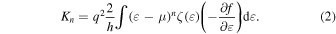
Here, q, h, and f are charge of the carriers, Plank's constant, and the Fermi-Dirac distribution function, respectively μ, which is the chemical potential of the system, can be experimentally controlled by carrier doping.6,7,11–13) In the present paper, we focus on the "lightly hole-doped" regime of  However, it should be noted that the behavior in the "lightly electron-doped" regime would be essentially the same owing to the nearly symmetric band structures of SWCNTs for hole and electron doping.
The power factor (P) is usually defined as

where σ is the electrical conductivity. However, P in the present paper is defined instead as

where S and G are the Seebeck coefficient and the electrical conductance  for individual SWCNTs, respectively. This is the power factor per SWCNT.
Next, using the results for the individual SWCNTs, laterally aligned parallel circuits of SWCNTs18) as illustrated in Fig. 1, with an m-SWCNT content β, were calculated. When there are two channels in parallel due to s-SWCNTs and m-SWCNTs, the  (
( ) value for the circuit is given by
  where the superscripts m and s denote the contributions from m-SWCNTs and s-SWCNTs, respectively. Thus, the corresponding Seebeck coefficient for the circuit can be expressed as
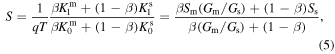
where  and
and  are the Seebeck coefficient and the electrical conductance for the individual intrinsic m(s)-SWCNT, respectively. The power factor P for the circuit is defined by Eq. (4) in the present paper. β is given by
 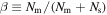 where
where  and
and  are the numbers of m- and s-SWCNTs in the circuit, respectively.
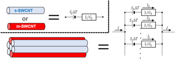
Fig. 1. (Color online) Illustration of an SWCNT bundle and its equivalent parallel circuit.  and
and  are the Seebeck coefficient and electrical conductance of the jth SWCNT in the bundle, respectively, and
  is a temperature difference applied to the bundle.18)
Download figure:
Standard image High-resolution imageFirst, we present the T dependence of S and G for an s-SWCNT with a chiral index (8, 0) and for an m-SWCNT with a chiral index (5, 5) in the lightly hole-doped region,  for several temperatures between 50 K and 500 K.
The results for the individual (8, 0) s-SWCNT are shown in Fig. 2(a). The top of the valence band is located at  It is found that G and S exhibit metallic and semiconducting behavior for
  and
and  respectively. For example, S and
  increase with decreasing T when μ is located in the semiconducting band gap,
  More specifically, the T dependence of S varies as
 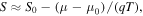 where
where  is a constant depending on
  around the band edge,
  This is a well-known behavior established in previous studies.17,18,21,22) On the other hand, S and G become metallic when μ is located within the valence band,
  S decreases and G approaches the value for m-SWCNTs with decreasing temperature.
Fig. 2. (Color online) The T dependence of G, S, and P for individual SWCNTs for μ values between  and
and  Squares with dashed lines and circles with solid lines are for
  and
and  respectively, where the top of the valence band for (8, 0) s-SWCNTs is located at
  (a) shows results for (8, 0) s-SWCNTs, and (b) for (5, 5) m-SWCNTs. The G of (5, 5) m-SWCNTs is almost independent of T and μ in (b). The third and second panels on the right of (a) and (b), respectively, show the electron DOS as a function of ε. The bottom panel on the right of (b) shows schematics of (5, 5) and (8, 0) SWCNTs.
Download figure:
Standard image High-resolution imageThe results for the individual (5, 5) m-SWCNTs are shown in Fig. 2(b). G is almost independent of T because the present calculation was performed in the ballistic regime. G is also independent of μ in the present μ region because of the assumption of ballistic transport. S decreases monotonically with decreasing T, i.e., it shows metallic behavior. However, its magnitude is substantially smaller than that for s-SWCNTs. This is expected on the basis of the Mott formula, which can be applied to metals:  Thus, in the case of m-SWCNTs, the diffusive contribution to S might be important.
Next, we present the results for parallel circuits consisting of (8, 0) s-SWCNTs and (5, 5) m-SWCNTs. The results for  are presented in Fig. 3(a). (The results for thick SWCNT circuits consisting of (22, 0) s-SWCNTs and (13, 13) m-SWCNTs are shown in Supplementary Data is available online at stacks.iop.org/APEX/13/015001/mmedia.) The results for
 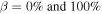 are essentially the same as those for the individual (8,0) s-SWCNTs and (5, 5) m-SWCNTs, respectively, which are shown in Fig. 2.
Fig. 3. (Color online) (a) T dependence of  and P for mixed parallel circuits of (8, 0) s-SWCNTs and (5, 5) m-SWCNTs with μ values between −0.60 and −0.40 eV. Left:
  Right:
  (b) μ dependence of S and P for T = 100 K, 300 K, and 500 K. The thick dotted lines indicate
  It is found that S shows a different T dependence below 500 K for
  S is T-independent for
  decreases monotonically for
  attains a maximum at 300 K for
  and increases monotonically for
  with rising temperature from 100 K to 500 K.
Download figure:
Standard image High-resolution imageAs expected, G for  increases with decreasing temperature for
  within the valence bands and decreases for μ within the band gap
 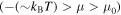 because it is dominated by the T dependence for the s-SWCNTs. However, the values at the lowest temperatures remain finite in all cases because G is limited by the metallic value for the s- and m-SWCNTs.
On the other hand, the  of the mixed parallel circuits is quite different from those of the pure s-SWCNT circuits. While the
  of individual s-SWCNTs monotonically increases with decreasing temperature for
  as shown by the dashed lines in Fig. 2(a), those in the mixed circuits are seen to show different behaviors depending on μ, and to exhibit a peak. The
  of the mixed circuits monotonically decreases with decreasing temperature at low temperatures, as explained by Eq. 5 for S of the mixed circuits. Because
  steeply decreases with decreasing temperature while
  and
and  are nearly constant,
  for
for 
The peak seen in the S–T relationship moves to higher temperature as μ is reduced to the top of the valence band,  The peak also moves to higher temperature with increasing m-SWCNT content, β. Such behavior is easily deduced from Fig. 3(b), where S is plotted as a function of μ for T values of 100 K, 300 K, and 500 K, and is seen to exhibit a peak. This can be inferred from the approximate form for
![$S\left(\mu \right)\,\approx \left[(1-\beta )/\beta \right]{S}_{{\rm{s}}}\left({G}_{{\rm{s}}}/{G}_{{\rm{m}}}\right),$](https://content.cld.iop.org/journals/1882-0786/13/1/015001/revision2/apexab547bieqn60.gif) which can be obtained for
which can be obtained for  and
and  in Eq. (5). Because
  and
and ![${G}_{{\rm{s}}}/{G}_{{\rm{m}}}\propto {G}_{{\rm{s}}}\propto \exp \left[-\left(\mu -{\mu }_{0}\right)/\left({k}_{{\rm{B}}}T\right)\right],$](https://content.cld.iop.org/journals/1882-0786/13/1/015001/revision2/apexab547bieqn64.gif) it is found that the
it is found that the  peak moves to higher μ values with increasing T. Thus, for appropriate μ values,
  exhibits a peak in the specific T range we examine. In Fig. 3(b), for example, a peak appears around 300 K for
Figure 3(b) also shows the power factor,  It is seen that the
  and
and  maxima are both independent of temperature. However, the μ values where the maxima appear increase with temperature.
The calculation results can be compared with the experimental results for SWCNT films with chemical doping.6) Figure 4(a) shows the T dependence of S for films enriched with s-SWCNTs. The nominal m-SWCNT content, β, was lower than  It is well known that pristine films are already p-type. Further p-type doping was achieved chemically using HCl, H2SO3, and HNO3, whereas annealing in vacuum led to de-doping, as shown in Fig. 4(d). Upon p-type doping, the film resistivity (ρ) decreases and S exhibits a peak corresponding to the change in μ. The S–ρ relationship has been well established in previous studies.11,18)
Fig. 4. (Color online) Comparison of (a) experimental results from Ref. 6 and (b) calculation results. Experiments were performed on s-SWCNT-enriched films. (c)  as a function of T. Solid lines are calculated values; dashed lines were used in order to reproduce experimental results. (d) S versus ρ at 300 K from the experiments.6) With p-type doping or decreasing μ, ρ decreases monotonically while S exhibits a peak. In the calculations, (b) and (c), β was assumed to be 5%.
Download figure:
Standard image High-resolution imageThe calculation results are shown by solid lines in Fig. 4(b) for fixed μ values. We found that the typical behavior observed for the annealed and pristine films in the upper panels is semi-quantitatively reproduced by calculation with  and
and  respectively. The results for the chemically doped films are also semi-quantitatively reproduced by calculation using
  for the HCl film and
  for the H2SO4 film (and the HNO3 film). It is important to note that the μ value used in the calculations consistently decreases with additional p-type doping or decreasing
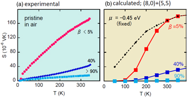
  as shown in Fig. 4(d). Similarly, the β dependence is reproduced well by the calculations (see Fig. 5). Therefore, the overall behaviors observed experimentally, such as the absolute values for S at room temperature and qualitative T dependence of S for different μ and β values, were reproduced well by the present calculations.
Fig. 5. (Color online) Comparison of experimental results taken from Ref. 6 (a) and calculated results (b). The dashed line in (b) shows S corrected by  as represented by the dashed line in Fig. 4(c).
Download figure:
Standard image High-resolution image
Recently, it was reported that  decreases with decreasing temperature irrespective of the carrier density or the Fermi level examined in high purity s-SWCNT samples.25) It might have failed to reproduce observations of the intrinsic behaviors for
  as shown by the dashed lines in Fig. 2(a) for
  This suggests the possibility of substantial effects which are related to impurity states and low metallic component inclusion in the samples.
Further inspection of Figs. 4 and 5, however, reveals that the experimental S values are substantially larger than the calculated values at low temperatures. This implies that S may be enhanced at low temperatures. There are several possible causes for this. Equation (5) indicates that S depends on the ratio  Thus, the deviation in
  from the calculations at low temperatures may be one possible cause. If it is assumed that the T dependence of
  is much weaker than that for the calculated results, as suggested by the dashed lines in Fig. 4(c), the observed S is reproduced well by the calculations using the corrected values for
  as shown by the dashed lines in Fig. 4(b). The deviation of
  from the calculated values may also be due to significant elastic and inelastic electron scattering,26,27) electron localization effects,28) or the SWCNT–SWCNT junctions. It appeared that the corrected
  obtained from the present analysis may be much lower than the values for the ballistic regime at low temperatures.
The enhancement of S at low temperatures may also stem from a diffusive contribution to S, a phonon drag effect,29) inhomogeneity of the SWCNT diameter and the doping level, and a bundle effect or deviation from the one-dimensionality of the electronic states in SWCNTs. Further discussion on this issue, including T dependence of μ, is left for future study.
In conclusion, it was found that the T dependence of S in mixed s- and m-SWCNT films could be semi-quantitatively explained by a bundle model of parallel circuits of s- and m-SWCNTs. Calculations for the parallel model demonstrated that a low proportion of m-SWCNTs modifies substantially the T dependence of S from that of ideal pure s-SWCNT bundles. The highest values for S and P in a mixed film appeared at different doping levels, μ, depending on the temperature, while the maximum values showed little dependence on temperature. It also appeared that S is greatly enhanced at low temperatures.
Acknowledgments
Y. Maniwa acknowledges valuable discussions with Prof. Takahiro Yamamoto on calculation details using the ATK software. This work was supported in part by JSPS KAKENHI Grant Numbers 18K13518, 25800201, 15K04601, 18K03545. K. Y. acknowledges support from JST CREST through Grant Number JPMJCR17I5, Japan. Y. Miyata also acknowledges support from JST CREST through Grant Number JPMJCR16F3, Japan.