

Abstract
We proposed solvent-free cross-linked ion gel polymer as a high-κ gate dielectric composed with polyurethane terminated with acrylate functional group and ionic liquids (1-Ethyl-3-methylimidazolium bis(trifluoromethylsulfonyl)imide) through ultra violet curing (UV-cured IL-PU). Free-standing UV-cured IL-PUs were applied as gate insulator by conformally contacting on the amorphous indium gallium zinc oxide side-gate structure thin film transistor with a simple ex situ method. The device shows a dramatic improvement of electrical performances even under low operating voltage conditions; on/off ratio ∼104, field effect mobility at linear region 47.79 ± 17.65 cm2 V−1 s−1, sub-threshold swing 145.54 ± 16.65 mV decade−1 at VDS = 0.1 V and VGS sweep from −3 to 2 V.
Export citation and abstract BibTeX RIS
Wearable and portable mobile electronic devices (such as virtual reality technology, smart watches, smart glasses, etc.) are required in variety of areas.1) Since these devices are driven using a limited voltage source, power consumption is the important issues as well as performance. One of the major components of the electronic device, the thin film transistor (TFT) is directly involved in driving the device. Therefore, many researchers are working on various aspects to improve the performance of the TFT.2) In particular, transparent amorphous oxide semiconductor based TFTs are believed to contribute significantly to the next generation electronics industry by providing low leakage current, high transparency, and high field effect mobility despite amorphous phase compared to conventional amorphous silicon TFTs.3–5) Among them, the performance of indium gallium zinc oxide (IGZO)-based TFTs reached the state of art and shows high field-effect mobility (∼10 cm2 V−1 s−1), low off current (∼pA) and relatively low sub-threshold swing (∼0.2 V decade−1) thus it is applied directly to commercialization.6) However, when SiO2 is used as a gate insulator, an operating voltage of 20 V or more is required to achieve the above performance, so the IGZO TFT is still limited to a fixed display such as TV, electronic display board and so on.7)
Recently, in order to further improve the drive current at low operating voltage for low-power consumption, the gate insulator in TFTs have been considerably focused.8–11) One strategy to increase the drain current (IDS) of a transistor based on traditional metal-oxide-semiconductor field effect transistor (MOSFET) theory is to increase the capacitance (Ci) of the gate insulator based on the IDS ∝ Ci relationship from the metal–insulator–semiconductor region. Specially, in case of on TFTs including amorphous oxide semiconductors, the IDS behavior of TFTs based strongly depends on the power series of Ci, since disordered metal ions and dense grain boundaries directly affect the total number of accumulated charge carriers in the channel, thus the IDS is not linearly related to Ci.12) This suggests that a high-κ gate insulator should be considered in more depth in the amorphous oxide semiconductor-based TFT.
In the case of the high-κ oxide insulator so far reported, the trade-off relationship is evident in the correlation between the band gap (4–8 eV) and κ (4–20).9) To overcome these issues, a number of studies have been introduced using ionic liquids (ILs) as gate insulators.13–21) In 2008, Frisbie et al. show that a new class of polymer electrolytes, known as ion gels, can serve as printable high capacity gate insulators for thin film transistors.22) ILs feature a very large specific capacitance because they form a nanometer-thick electrical double layer (EDL) at the dielectric/semiconductor interface. Furthermore, when an IL having an ionic conductivity but an electrically insulating property is used as a gate dielectric, the number of charge carriers of the transistor channel can be effectively increased. In addition, due to its high dielectric constant, it can operate at lower power than other types of gate insulators.
However, since ILs exists in liquid, it has a serious problem that it is difficult to apply ILs directly to a TFT. To overcome this problem, many researchers used the polymer as the framework of ILs. Most studies have used solvents to apply ILs/polymer composite, or ion gels.23,24) Meanwhile, when solvents were used, there are various problems caused by residual solvents such as substrate contamination and uneven membrane formation etc.25)
Here in, we proposed the solvent-free ion gel polymer as a high performance gate dielectric composed with polyurethane terminated with acrylate functional group (PUA) (Mw: ∼ 11 000 g mol−1) and 1-ethyl-3-methylimidazolium bis(trifluoromethylsulfonyl)imide (EMITFSI) through ultra violet (UV) curing. Specially, the PUA shows a fluidic form as an oligomer, so it features solventless UV curable properties and good compatibility induced by hydrogen bonding with EMITFSI. In addition, EMITFSI shows that by forming an EDL at the interface with oxide semiconductors providing high density charge carrier accumulation at the channel, so that the actual TFT can operates at very low voltages. Additionally, we propose UV curable hexa-acrylate PU as encapsulation material, which shows a good durability in high relative humidity and high temperature. The IGZO TFTs including the proposed UV-cured EMITFSI-PU (IL-PU) shows a dramatic improvement of electrical performances and average values as follows; field effect mobility at linear region 47.79 ± 17.65 cm2 V−1 s−1, sub-threshold swing 145.54 ± 16.65 mV decade−1 at VDS = 0.1 V and VGS sweep from −3 to 2 V.
Figure 1(a) shows the prepared UV-cured IL-PU chemical structures. Black part is UV-cured PU, red part is EMITFSI. After UV curing, a PU–PU covalent bond is generated, while a hydrogen bond (blue dashed line) is generated between urea groups in the cured PU and nitrogen of EMITFSI.26,27) Their structures are confirmed with ATR-FTIR spectroscopy (BRUKER, Alpha) at 4000–600 cm−1 ranges as described in Fig. 1(b). Stretching peaks of CH bond from PU were observed at 2969–2847 and 1380 cm−1. Moreover, the –NH group banding for PU was observed at 1522 cm−1 and –NH stretching peak was noticed at 3336 cm−1, 3382 cm−1, and 3389 cm−1 for PUA, IL-PU mixture, and UV-cured IL-PU, respectively [Fig. S1(a) is available online at stacks.iop.org/APEX/12/101004/mmedia]. NH stretching peaks was blue shifted by EMITFSI. These results show that hydrogen bonding formed between EMITFSI and PU where the hydrogen donor is PU and the acceptor is the F, O atom of EMITFSI. The peaks observed near 1637 cm−1 are the C=C bonding stretching peaks of acrylate. As shown in the Fig. S1(b), it was observed that the peak had disappeared after the IL-PU UV curing, which confirmed that the UV curing process had been successful. Figure S2 shows the optical image before and after UV curing of IL-PU. The UV-cured IL-PU became a "free standing" film that can maintain its shape without relying on the substrate by causing a significant phase change from the liquid phase to the solid phase. Figure 1(c) exhibits thermal stability, and thermal decomposition temperatures were analyzed from onset temperature which mean that the cross point of the tangent line to the decrement starting portion and base line (initial flat section) in the TGA graph by extrapolation. Prepared UV-cured IL-PU were thermally stable over 300 °C which means it can enhance thermal stability of TFTs. The first pyrolysis occurred at 345.64 °C and the second pyrolysis appeared around 448.4 °C. Considering the thermal decomposition temperature and weight ratio of PU and EMITFSI, the first thermal decomposition was affected by PU, and the second was derived from EMITFSI. Although cured PU is thermally degraded at 318.9 °C, UV-cured IL-PU were thermally stable up to 345.64 °C. The hydrogen bonding between EMITFSI and PU increased the thermal degradation temperature of cured IL-PU and enhanced the thermal stability of UV-cured IL-PU. The frequency dependence of specific capacitance of the 150 μm thick UV-cured IL-PU was measured with an AC impedance analyzer (biologic SP510). The analysis was performed with an AC amplitude of 5 mVrms at open circuit voltage [Fig. 2(a)]. As is widely known, ILs enable EDL formation due to high ionic conductivity, and are known to have the same capacitance regardless of thickness. This characteristic is highly encouraging for applying dielectric areal capacitance values when calculating field effect mobility in TFTs with side gate structures. Therefore, we first measured the areal capacitance with respect to frequency in each MIM structure by varying the thickness of IL-PU to 140, 180, 250, and 400 μm [Fig. 2(b)]. As a result, the same capacitance value was obtained regardless of thickness within the range of 10 mHz to 45 kHz, which is the same as the tendency of previous studies. The areal capacitances of four thickness conditions at 10 kHz were 1.54 ± 0.052 μF cm−2 which are considerable capacitance comparing with the most widely used 200 nm thick SiO2 specific capacitance of ∼17 nF cm2 (Fig. S3). It is thought that this large capacitance is due to the EDL generated at the interface between the electrode and the ILs. It is also indirectly demonstrated that the UV-cured PU framework and the ILs are stable hydrogen bonds, since a high uniformity of capacitance is maintained up to the high Hertz interval. These results indicate that the application of the IL-PU dielectric can eliminate structural parameters to be considered in calculating field effect mobility in the side gate TFT devices. Therefore, we define the channel width and length of the side gate TFT in the same view as the bottom gate structure, and are 1600 μm and 100 μm, respectively. The spacing between the source-drain, and gate electrodes was 150 μm, and the thickness of the IL-PU dielectric we applied to the device was also 150 μm, which means that the results of the areal capacitance experiments for each thickness of the dielectric can be equally applied.
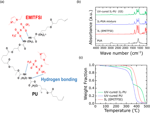
Fig. 1. (Color online) Material properties of UV-cured IL-PU. (a) Chemical structures of prepared UV-cured IL-PU. Black part is UV-cured PU, red part is EMITFSI. (b) ATR-FTIR analysis of PUA, IL (EMITFSI), IL-PUA mixture, UV-cured IL-PU. (c) TGA analysis of IL (EMITFSI), UV-cured PU, UV-cured IL-PU.
Download figure:
Standard image High-resolution image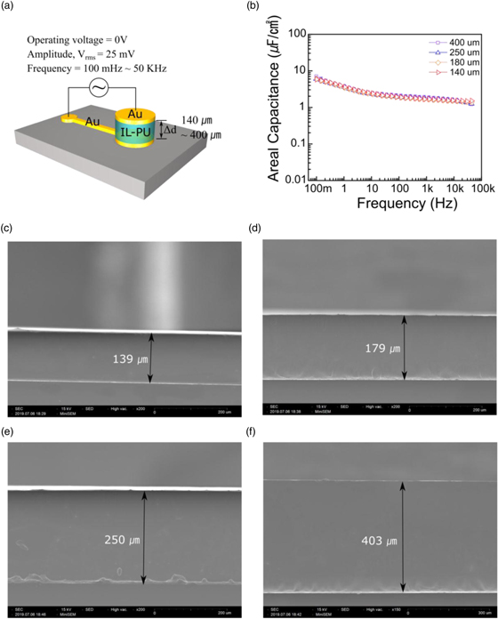
Fig. 2. (Color online) Frequency dependence of areal capacitance of UV-cured IL-PU varying with the thickness. (a) Structure of the IL-PU areal capacitance analysis. (b) Frequency-areal capacitance plot of UV-cured IL-PU varying with the thickness. (c)–(f) Cross section SEM images of UV-cured IL-PU varying with the thickness. (c) 140 μm (d) 180 μm (e) 250 μm (f) 400 μm.
Download figure:
Standard image High-resolution imageFigure 3 shows the electrical characteristics of the IGZO TFT using UV-cured IL-PU as a gate insulator. IGZO was deposited on a 200 nm SiO2 on P++ Si substrate by a sputtering system, and source drain and gate electrode were used to deposit aluminum. UV-cured IL-PUs were fabricated by using the ex situ method as a simple patch to form conformal contacts on source, drain, and gate electrodes [Fig. 3(a)]. Figure 3(b) shows the charge carrier accumulation model induced in the IGZO layer by the EDL and the location of the EDL formation. The transfer curve of the device was obtained with VDS = 0.1 V and VGS sweep from −3 to 2 V [Fig. 3(c)]. The on/off ratios of 2.94 × 10⁴, low sub-threshold swings of 171.59 mV decade−1, and μ(FE,lin.) were surprisingly boosted to 44.91 cm2 V−1 s−1 even under narrow gate drive voltages and low drain voltage conditions. The field-effect mobility (μ) in the linear region was evaluated from the trans conductance (gm) as following equations.28)

where, W and L are the width (1600 μm) and length (100 μm) of the channel, respectively, and Ci is the capacitance of the insulator. The gate electrode was laterally positioned at a gap distance of 150 μm laterally perpendicular to the source and drain electrodes, which coincidentally corresponded with the thickness of the IL-PU insulator (150 μm). The Ci value applied to derive the field effect mobility is 1.54 μF cm−2, which is the capacitance value under 10 kHz condition. On the other hand, in case of IGZO TFT using SiO2 dielectric of the normal bottom gate structure, IGZO performance was maximized by setting VDS = 50 V and VGS sweep to −50 to 50 V, and showed 7.72 cm2 V−1 s−1 of μ(FE,sat.). The results confirm that the IGZO thin film has a generally reliable quality (Fig. S4 and Table S1).
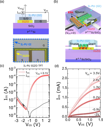
Fig. 3. (Color online) Electrical characteristics of the IGZO TFT using UV-cured IL-PU as a gate insulator. (a) Device scheme and driving circuit of UV-cured IL-PU IGZO TFT. (b) Location of EDL formation when the device is driven and a model in which charge carriers accumulate in the IGZO channel part due to the formation of the EDL. (c) Transfer curve of IL-PU IGZO TFT. VDS = 0.1 V, VGS = −3 to 2 V. (d) Output curve of IL-PU IGZO TFT. VGS = −2, −0.9, 0.2, 1.3, 2.4, 3.5 V, VDS = 0–1.5 V.
Download figure:
Standard image High-resolution imageAs a result, IGZO TFTs with a side gate structure using IL-PU (gap spacing of source-drain electrode to gate electrode: 150 μm) as an insulator shows 13 times higher field effect mobility than IGZO TFTs with a bottom gate structure using SiO2 (gap spacing of source-drain electrode to gate electrode: 200 nm). This means that the influence of EDL formed on the gate insulator–semiconductor, gate electrode-gate insulator interface by ILs is dominant.19) Due to the high ionic conductivity of the ILs, when the TFT is in the accumulation mode, the charge carriers are accumulated in the channel of the IGZO and gate insulator interface excessively and the drain current is boosted [Fig. 3(b)]. The high drain current can be ensured in a narrow voltage window, so that the field effect mobility can also be effectively boosted. The main goal of this study is to show that IL-PU dielectric fabricated by solvent-free process under atmospheric conditions can be stably applied as a gate dielectric of TFT. Since the IL-PU dielectric is fabricated under atmospheric conditions, the gate leakage current is relatively high when the dielectric is applied to the TFT than the conventional oxide insulator manufactured by the vacuum process. However, IL-PU TFT has a gate leakage current level similar to that of other polymer dielectric TFTs reported by various researchers. Nevertheless, future research on the establishment of IL content conditions will be needed to ensure the relatively low leakage current while taking advantage of IL-PU, which is the simple fabrication with solvent-free process at atmospheric conditions. The results of the above-mentioned IL-PU/IGZO device is the average performance data in this study, and the field effect mobility of 15 devices using the same UV-cured IL-PU dielectric follows the Gaussian distribution and average value of μ(FE,lin.) is 47.79 ± 17.65 cm2 V−1 s−1 (Fig. S5 and Table S2). In order to more universally evaluate the effect of IL-PU gate insulator, we have conducted further experiments using a device showing μ(FE,lin.), of ∼90 cm2 V−1 s−1.
For the wider utility of our proposed gate dielectric material, we evaluated the possibility of an encapsulation layer by applying intrinsic UV-curing a hexa-acrylate PU on the IL-PU. Figure 4 shows the result of exposure of the IL-PU IGZO TFT with and without encapsulation layer in a relative humidity (RH) 85% and 85 °C for 24 h. The IL-PU IGZO TFT without encapsulation underwent considerable deterioration of the device after 24 h at RH-85% and 85 °C. The device completely deteriorated that μ(FE,lin.) dramatically changed from 40.91 to 0.35 cm2 V−1 s−1 [Figs. 4(a) and 4(c)]. Under extremely severe conditions, moisture penetrates into the interface between gate insulator and IGZO, causing excessive oxidation of the oxide semiconductor. On the other hand, in case of UV-cured IL-PU IGZO TFT with PU encapsulation, there was no significant difference between results before and after 24 h at RH-85%, 85 °C. μ(FE,lin.) slightly changed 47.03–44.91 cm2 V−1 s−1, demonstrating that the UV-cured PU performed almost perfectly as an encapsulation layer [Figs. 4(b) and 4(d)].

Fig. 4. (Color online) RH 85%, 85 °C at 24 h testing with and without PU encapsulation. (a) Transfer curve of IL-PU IGZO TFT without PU encapsulation. (b) Transfer curve of IL-PU IGZO TFT with PU encapsulation. Comparison of field effect mobility (linear region) change before and after RH 85%, 85 °C at 24 h testing (c) without and (d) with PU encapsulation TFTs.
Download figure:
Standard image High-resolution image
See supplementary material for experimental methods section of this work. Tables and figures of structure analysis and electrical characteristics, frequency dependence of areal capacitance, field effect mobility distribution of devices are included.
In summary, we proposed solvent-free cross-linked ion gel polymer as a high-κ gate dielectric composed with polyurethane terminated with acrylate functional group (PUA) (Mw: ∼11 000 g mol−1) and ionic liquids (EMITFSI). PUA has realized a solventless UV curable process and it is highly compatible with such hydrogen bonding as EMITFSI. It can be applied as a gate dielectric through ex situ method very simply after UV-curing, helping to free-stand without leakage of the IL due to strong hydrogen bonding. At the same time, ILs with high ionic conductivity and electrically insulating properties form a nanometer-thick EDL at the insulator-oxide semiconductor interface, so that when the TFT is in accumulation mode, it has played a key role in boosting field effect mobility. The IGZO TFTs including the proposed UV-cured EMITFSI-PU (IL-PU) shows a dramatic improvement of electrical performances even under narrow gate drive voltages and low drain voltage conditions; on/off ratio ∼104, field effect mobility at linear region 47.79 ± 17.65 cm2 V−1 s−1, sub-threshold swing 145.54 ± 16.65 mV decade−1 at VDS = 0.1 V and VGS sweep from −3 to 2 V conditions. Moreover, for the wider utility of our proposed gate dielectric material, we evaluated the possibility of an encapsulation layer by applying UV-curing a hexa-acrylate PU with no ILs on the gate dielectric. In the PU encapsulated device, μ(FE,lin.) was slightly changed 47.03–44.91 cm2 V−1 s−1 before and after 24 h at RH-85% and 85 °C, thus the UV-cured PU acts as robust encapsulation layer. We believe that our proposed gate insulator and encapsulation material will provide stable low-voltage operation and high performance for organic–inorganic hybrid TFTs.
Acknowledgments
This work was supported by the National Research Foundation of Korea (NRF) grant funded by the Korea government (MSIT, Ministry of Science and ICT)—Basic Science Research Program [2019R1A2C1009239] and Nano-Material Technology Development Program [2016M3A7B4910458]. Also, it was supported by LG Display Academic Industrial Cooperation Program.