

Abstract
We report a plasma damage removal method for β-Ga2O3 devices using hot phosphoric acid solution. Sidewall Schottky diodes were fabricated on MOCVD-grown un-intentionally doped β-Ga2O3 films grown on (010)-oriented semi-insulating substrates. Removal of the plasma damaged layers using wet etching resulted in near unity ideality factor and reduced hysteresis. The anisotropic etching behavior on the electrical characteristics of the devices was further evaluated, and the [001] direction was found to be a favorable direction for vertical device fabrications. The demonstrated damage removal method could enable a range of novel device architectures, including high power vertical diodes, vertical transistors and ultra-scaled devices.
Export citation and abstract BibTeX RIS
β-Ga2O3 has recently attracted significant research interest because of its excellent intrinsic material properties, including the wide bandgap energy of 4.8 eV,1) the high breakdown field projected near 8 MV cm−12) and the feasibility of n-type doping and contacts.2–4) The availability of high quality bulk substrates5,6) also ensures excellent device reliability under high electric field stress, making β-Ga2O3 especially promising for power switching applications. However, a significant drawback of the material system is the lack of p-type conduction because of a nearly flat energy dispersion profile in the valence band.7,8) As a result, several unipolar device topologies have been investigated extensively, including both lateral transistors (MESFETs,2,9) MOSFETs,10–15) MODFETs16–19)) and vertical devices (Schottky diodes20–23) and vertical MISFETs24)). Excellent device results with high breakdown voltage above 1 kV have been demonstrated for various device topologies.22,24–26) However, the electrical properties of the β-Ga2O3 films was found to be sensitive to plasma damage,14,27) and this brings significant challenges for the fabrication of novel device architectures. For instance, gate recess by inductively coupled plasma (ICP) etching has contributed to a substantial reduction of the channel mobility from 80 to 34 cm2 V−1 s−1 for Si delta-doped MOSFETs.14) Additionally, both vertical MISFETs24) and lateral fin-channel MOSFETs28) with thin channels defined by BCl3-based plasma etching demonstrated low field effect mobility and high on-resistances, indicating signs of plasma damage-induced reduction of the electrical conductivity. Removal of the plasma damaged layer and sustaining low defect density after device fabrication is therefore essential for the realization of high performance β-Ga2O3 power switching devices.
Chemical wet etching has been utilized as an effective method for the removal of dry etching damages for a range of semiconductor devices, including TMAH etching for GaN vertical transistors,29) and thermal oxidation and subsequent HF etching for both Si30) and SiC31) devices. However, wet etching methods have not been explored for the etch damage removal for β-Ga2O3 devices. While β-Ga2O3 is chemically unreactive at room temperature, it can be etched effectively in heated H3PO4, HNO3 or H2SO4 solutions with an etch rate up to a few microns per hour.32,33) Recently, we observed strong anisotropic etching behavior of β-Ga2O3 in hot H3PO4 solutions, which provides a great opportunity for the fabrication of ultra-scaled vertical devices with low sidewall damage. In this work, we report improved performance for lateral Schottky diodes fabricated on MOCVD-grown un-intentionally doped (UID) films through sidewall damage removal using hot phosphoric acid etch.
The UID β-Ga2O3 films were grown in an Agnitron Technology Agilis R&D MOCVD system.34,35) A 3.2 μm thick epi-layer was grown at a rate of 0.8 μm h−1 on 10 × 15 mm2 (010)-oriented Fe-doped semi-insulating substrates from Novel Crystal Technology, Inc. The samples showed smooth surface morphology with rms surface roughness in the range of 0.5–0.8 nm for 20 × 20 μm2 AFM scans. Both Hall measurement and capacitance–voltage measurement indicate a low free carrier concentration of 1 × 1016 cm−3 in the UID β-Ga2O3 layer. For the fabrication of lateral Schottky diodes, a 15 nm heavily doped n+-Ga2O3 contact layer was grown on the MOCVD-grown UID β-Ga2O3 film using oxygen plasma-assisted molecular beam epitaxy.36) Sn was used as n-type dopant for the contact layer with a doping concentration of 3 × 1019 cm−3 as estimated from secondary ion mass spectrometry measurement.
The sample was diced into 5 × 5 mm2 pieces and further fabricated into sidewall Schottky diodes as shown in Fig. 1. A 350 nm SiO2 layer was first deposited on the sample surface using plasma-enhanced chemical vapor deposition to protect the top surface of the β-Ga2O3 film from any etch damage. Then, deep mesa structures with a dimension of 80 × 25 μm2 were patterned using BCl3-based ICP etching.37) Surface profile measurement using Dektak confirmed an etch depth of 3.4 μm in the β-Ga2O3 film, which ensured complete removal of the 3.2 μm MOCVD-grown UID layer. To investigate the effect of anisotropic wet etching of the sidewalls on the Schottky diode performance, the long edges of the mesa structures were aligned to different [h0l] crystal orientations on the same sample. This was followed by wet etching of the samples in hot phosphoric acid (w.w. > 85%) at 140 °C as measured and feedback controlled by a thermocouple. Two samples with etch times of 6 and 12 min and a control sample without wet etching were prepared. Figure 2 shows the bird's eye SEM images measured at a tilt angle of 60° after different fabrication steps, as well as the illustrating schematics. Direct dry etching resulted in rough sidewalls as shown in Fig. 2(a). The sidewall SEM image of a device aligned to [001] direction for the sample wet etched in hot H3PO4 solution for 12 min is shown in Fig. 2(b), which demonstrated a significant reduction of the sidewall roughness. Additionally, the lateral etch removal of the [001]-oriented sidewalls is estimated to be 134 nm and 268 nm for 6 min and 12 min etches, respectively, making it possible to remove the dry etch damage.

Fig. 1. (Color online) Fabrication flow for the sidewall Schottky diodes on MOCVD-grown UID β-Ga2O3 films.
Download figure:
Standard image High-resolution image
Fig. 2. (Color online) SEM images and the corresponding schematics for the sidewall after different fabrication steps: (a) after ICP dry etch for 3.4 μm, (b) after wet etch for 12 min, (c) schematic for (a) and (b). (d) Sidewall Schottky diode fabricated without wet etch. (e)–(f) Tilted and cross-sectional SEM images of the sidewall Schottky diode along [001] direction fabricated after 12 min wet etch in 140 °C H3PO4 solution. Uniform Schottky contact coverage was obtained on the etched sidewalls. The thick Pt layer on the device shown in (f) was deposited as a protection layer for focused ion beam (FIB) sampling.
Download figure:
Standard image High-resolution imageThe Pt/Au (=40/30 nm) Schottky metal stack was deposited on the samples using e-beam evaporation with a planetary rotation setup, which enabled metal coverage on vertical mesa sidewalls. The metal layers on the top of the mesas were then lifted-off by the removal of the SiO2 protection layer using buffered HF solution immersed in ultra-sonic bath. The samples etched in hot H3PO4 solutions were found to be especially favorable for the lift-off process because of the undercut formation through lateral sidewall etching as schematically shown in Fig. 1. Finally, a Ti/Au (= 30/120 nm) metal stack was deposited on the top of the mesa, followed by a rapid thermal annealing at 500 °C in N2 ambient, to define ohmic cathode contact. To avoid sidewall Schottky contact to the heavily doped thin contact layer, the sample without phosphoric acid etching was then blankly etched for 18 nm using low power plasma etching. The SEM images of the devices post-fabrication are shown in Figs. 2(d) and 2(e). The Pt/Au Schottky contact remained on the sidewalls and there was a clear separation between the anode and cathode contacts. This was further confirmed by the cross-sectional SEM image shown in Fig. 2(f). Since the mesa structures were electrically isolated from the semi-insulating substrate, the fabricated lateral Schottky diodes provided a direct measurement of the sidewall properties.
The electrical characteristics of the sidewall Schottky diodes were compared for the samples without and with wet etching. Since a strong anisotropic etching behavior was observed for the sidewalls and this translated to differences in the electrical characteristics, the electrical performance of the devices aligned to [001] direction will be discussed first. A summary of the anisotropic behavior will be given at the end of the report.
The capacitance–voltage characteristics measured at 1 MHz of the sidewall Schottky diodes for the samples without wet etching and with a 12 min wet etching are compared in Fig. 3. The device without wet etching showed a large hysteresis with a voltage shift (∆V) up to 1 V between the forward and reverse scans. In comparison, the hysteresis for the [001]-oriented devices became negligible after sidewall etching, suggesting a significant reduction of the density of damage-induced traps through wet etching. 1/C2 is expected to have a linear dependence on the applied bias for ideal Schottky diodes, and the Schottky barrier height could be extracted from the intercept on the voltage axis. While both samples could show deviations from the ideal case because of the highly non-uniform electric field profile, the sample without wet etching projected a substantially higher Schottky barrier height. This again indicates the existence of a parasitic capacitance because of interface defects formed after dry etching. The CV measurements showed negligible frequency dispersion for both the capacitance and conductance of the Schottky diodes in the frequency range from 1 kHz to 1 MHz. Therefore, the traps introduced by plasma damage could have a lifetime longer than 1 ms. Estimation of the trap density is challenging for the sidewall Schottky diodes due to the non-uniform electric field profile and the difficulty in the determination of the anode area. Further studies on the trap spectrum and the extraction of interface trap densities will be investigated.

Fig. 3. (Color online) CV characteristics of the sidewall Schottky diodes fabricated without wet etch (a) and with 12 min wet etch in 140 °C H3PO4 solution (b).
Download figure:
Standard image High-resolution imageThe current–voltage characteristics of the devices without wet etching is shown in Fig. 4. The device showed low reverse leakage current. However, the forward current showed strong hysteresis especially in the subthreshold region, which exhibited two distinct slopes and a positive voltage shift above 0.8 V between the forward and reverse voltage scans. The lower current in the subthreshold region during reverse scan is attributed to reduced trap assisted tunneling due to a larger depletion width. For the forward scan, the traps were empty initially and get filled during the forward voltage sweep, while the reverse scan started with traps being filled and the trapped electrons got emitted gradually during the scan. Because of the long trapping and emission lifetime, more traps could remain filled in the subthreshold region during the reverse scan. When traps are filled with electrons, the trapped negative charge reduces the net charge density in the depletion region to ND+–Nt− as shown schematically in Fig. 4(c), where ND+ is the activated donor concentration and Nt− is the trapped electron density in the depletion region. As a result, the same voltage bias leads to an increase in the depletion width during reverse voltage sweep, which then reduces the shunt leakage current through trap assisted tunneling in the subthreshold region as shown in Fig. 4(a). This also contributed to a better ideality factor of 1.7 for the reverse scan, as compared to 2.1 for the forward scan as shown in Fig. 4(b). However, both values are substantially worse than that for planar Schottky diodes20–22,38) because of the existence of sidewall etch damages.
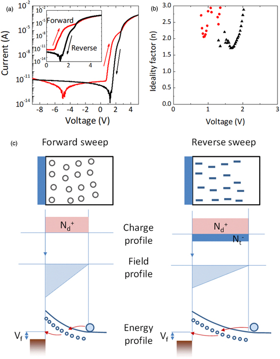
Fig. 4. (Color online) (a) IV characteristics and (b) ideality factor of the sidewall Schottky diodes fabricated without wet etch. (c) Charge, electric field and schematic energy band diagrams when the Schottky diode is biased in the subthreshold region for both forward and reverse voltage sweeps. More electrons could be trapped in the depletion region during reverse voltage sweep, leading to larger depletion width and therefore reduced shunt leakage through trap assisted tunneling.
Download figure:
Standard image High-resolution imageThe IV characteristics of the devices aligned to [001] direction after 12 min etching in hot H3PO4 are shown in Fig. 5(a). Apart from the low leakage current at reverse bias, the device showed negligible hysteresis and a clean subthreshold current. The ideality factor has a lowest value of 1.01, and it remained below 1.03 over 5 decades of the subthreshold current, suggesting a low trap density after sidewall etching in hot phosphoric acid.
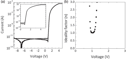
Fig. 5. (a) IV characteristics and (b) ideality factor of the sidewall Schottky diode along [001] direction fabricated with 12 min wet etch in 140 °C H3PO4. The devices showed ideality factor of 1.01 and absence of hysteresis.
Download figure:
Standard image High-resolution imageThe anisotropic behavior of the devices aligned to different crystal orientations is summarized in Fig. 6. Because of the strong anisotropic etch rate of the sidewalls and the differences of the sidewall roughness after wet etching, both the ideality factor and the hysteresis of the applied bias showed variations for the devices. The sidewall etch rate of the devices in 140 °C H3PO4 solution are shown in Fig. 6(a). The etch rate varies from 0.2 to 2.2 μm h−1 for different sidewalls. Most of the devices showed a positive correlation between the etch rate and the improvement of both the ideality factor and the subthreshold voltage hysteresis as shown in Fig. 6. The devices along [001] directions showed near unity ideality factor and low hysteresis after 6 min of wet etching because of the high lateral etch rate of the sidewalls. However, the devices aligned in the angular range between [203] and [201] directions showed high ideality factor after 6 min wet etching regardless of the higher etch rates. SEM measurement indicated slight roughening of those sidewalls rather than the smooth sidewalls observed for [001] oriented devices, and therefore, it could contribute to the high ideality factor. Longer etching resulted in near ideal sidewall Schottky diodes for the devices along almost all the directions. Those results suggest that wet etching in hot phosphoric acid could be an effective technique to remove the plasma damaged layers and recover a pristine surface for device fabrications.

Fig. 6. (Color online) (a) Sidewall etch rate in heated H3PO4 solution (140 °C) for the fins aligned to different orientations. (b) The ideality factor and (c) voltage hysteresis after 6 and 12 min wet etch in hot phosphoric acid solution.
Download figure:
Standard image High-resolution image
To conclude, we demonstrated an etch damage removal method for β-Ga2O3 devices using hot H3PO4 solution. Sidewall Schottky diodes were fabricated on a MOCVD-grown UID β-Ga2O3 film. The devices without wet etching for plasma damage removal showed high ideality factor and large hysteresis in both IV and CV measurements. Through wet etching in phosphoric acid heated at 140 °C, the sidewall Schottky diodes showed near unity ideality factor of 1.01 and absence of hysteresis. The anisotropic etching behavior of β-Ga2O3 was also evaluated. While the devices along various directions showed improved performance, the [001] direction was found to be a favorable direction for vertical device fabrications. The demonstrated anisotropic wet etching method for etch damage removal could be beneficial for various device applications, including vertical transistors and diodes, ultra-scaled devices, and it could enable a new paradigm of damage-free nano-electronics for β-Ga2O3.
Acknowledgments
The work at UCSB was supported by AFOSR through programs FA9550-18-1-0059 and FA9550-18-1-0479. Additional support at UCSB was provided through a subcontract from Agnitron Technologies through ONR program N00014-16-P-2058 and from DTRA through program HDTRA 11710034. Support at Agnitron was provided by AFOSR and ONR programs through grant numbers of FA9550-17-P-0029 and N00014-16-P-2058, respectively.