

Abstract
A simple structure with high breakdown voltage and a low leakage current of a vertical GaN p–n diode on a GaN free-standing substrate is demonstrated. We describe a vertical p–n diode with a simple edge termination that has a drift layer etched deeply and vertically. A device simulation revealed that the electric field was more relaxed at the device edge and applied uniformly in the entire device with increasing etching depth. We fabricated the simulated structure and succeeded in reducing the leakage current and improving the breakdown voltage. With this structure, a stable avalanche breakdown can be observed.
Export citation and abstract BibTeX RIS
GaN is a promising material for next-generation semiconductor power devices owing to its wide band gap, high breakdown electric field, and high-electron mobility. As new power devices have started to replace silicon power devices, which have reached the physical limits of silicon, lateral devices using GaN, typified by high-electron-mobility transistors, have been researched and commercialized. However, GaN power devices such as these lateral devices are normally grown on foreign substrates including sapphire, Si, and SiC substrates, and thus the dislocation density can reach approximately 108 to 1010 cm−2 owing to lattice mismatch. Although GaN power devices should potentially have a higher breakdown voltage than SiC power devices, owing to their higher dislocation density, GaN power devices could not exceed the performance of SiC devices.1–5) Recently, there has been significant progress in improving the quality of GaN free-standing substrates, and the dislocation density of commercially available GaN free-standing substrates is currently 104 to 107 cm−2. As a result, research on vertical GaN power devices with high breakdown voltage is progressing dramatically.6–11) However, GaN vertical power devices are still under development because of an unsatisfactory edge termination structure or a leakage current generation at dislocations.12–15) The unsatisfactory termination structure causes not only the leakage current owing to electric field crowding but also destructive breakdown and early avalanche breakdown at the device edge. Because of this problem, the impact ionization coefficient essential for predicting the breakdown field of GaN is still unknown. To reveal this physical property, it is necessary to realize a power device with high breakdown voltage and the capability of relaxing the electric field at the device edge and stable avalanche breakdown.16) To realize edge termination in GaN p–n diodes, a bevel mesa structure, a field plate structure, a guard ring structure, ion implantation, and other structures have been reported.17–24) In this letter, we report vertical GaN p–n diodes with simple edge termination structure that can obtain a uniform electric field to the entire device and a large electric field relaxation simply by deep and vertical mesa etching, and their capability of stable avalanche breakdown.
Figure 1(a) shows a schematic diagram of the p–n diode structure used for device simulation. A p–n diode comprising a 10 μm n-type GaN drift layer (Nd: 2 × 1016 cm−3), a 500 nm p-type GaN layer (Na: 2 × 1019 cm−3), and a 30 nm p+-GaN contact layer (Na: 2 × 1020 cm−3) on an n-type GaN free-standing substrate with a donor concentration of 2 × 1018 cm−3 and a deposited contact electrode was reproduced by a Silvaco ATLAS device simulator. Using this structure, the electric field distribution was simulated with the device simulator while varying the mesa depth. Figures 1(b)–1(f) show the images of the electric field distribution obtained by the simulation when a high reverse bias of −800 V was applied. The simulation shows that the electric field at the device edge becomes more relaxed and is applied more uniformly as the mesa is vertically etched to a greater depth. These results indicate that the dielectric breakdown at the device edge can be suppressed by etching the mesa to a greater depth than the depletion layer width at the designed breakdown voltage with a non-punch-through condition.
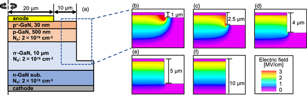
Fig. 1. (Color online) (a) Schematic cross section of the vertical GaN p–n diode used for simulation. (b) Simulated electric field distributions of the p–n diodes when a reverse bias of −800 V was applied for mesa depths of 1 μm, (c) 2.5 μm, (d) 4 μm, (e) 5 μm, and (f) 10 μm.
Download figure:
Standard image High-resolution imageFigure 2(a) shows a schematic diagram of the p–n diode structure that we fabricated. A p–n diode structure similar to that used in the simulation was epitaxially grown by metal-organic vapor phase epitaxy on an n-type GaN free-standing substrate. The GaN substrate was fabricated by hydride vapor phase epitaxy and had a threading dislocation density of 3.4 × 106 cm−2, measured by the wafer providers. Figure 3 shows secondary ion mass spectrometry profile of the growth layer. In the n-GaN drift layer, the concentration of silicon was 2.41 × 1016 cm−3 and the concentration of carbon was 1.52 × 1016 cm−3. The depth profile obtained by C–V measurement showed that Nd–Na was 1.9 × 1016 cm−3. The device fabrication process was as follows. The growth layer was etched by inductively coupled plasma-reactive ion etching (ICP-RIE) with pure Cl2 gas. ICP-RIE, which enables directional etching, was adopted to realize a vertical mesa structure. As an etching mask, Ni/Ti/Ni/Ti/Ni (50 nm/25 nm/100 nm/25 nm/100 nm) was deposited by electron beam (EB) vapor deposition and the mask was formed by a lift-off process. When only a thick Ni mask was deposited, the stress applied by Ni generated cracks in the photoresist and caused the failure of the lift-off process. The etching by ICP-RIE (CE-S, ULVAC) was performed at an antenna power of 150 W, a bias power of 15 W, and a Cl2 flow rate of 30 sccm. The etching rate of GaN under these conditions was approximately 1.5 nm s−1. The etching time was adjusted so that the etching depth of each device was 1, 2.5, 7.5, and 10 μm. The measured etching depths are 1.13, 2.29, 7.80, and 10.8 μm. The mesa diameters were 150–340 μm for each device. The p-type GaN layer was activated by rapid thermal annealing (RTA) in a nitrogen atmosphere at 700 °C for 5 min. A Ni/Au (20 nm /200 nm) anode was deposited by EB vapor deposition and formed by the lift-off process. Sintering annealing was performed in an oxygen atmosphere at 525 °C for 5 min by RTA. Subsequently, a 3.5 μm thick polyimide layer was coated to protect the side wall from a discharge in air. Patterning was performed by photolithography to form contact holes in polyimide. Finally, a bottom ohmic electrode was formed by depositing 200 nm Al by sputtering. Figures 2(b) and 2(c) show the cross-sectional scanning electron microscopy images of devices with the above structure fabricated by the same process. The side walls of these devices were passivated by alumina. By using the Ni/Ti layered etching mask, it was possible to realize a mesa structure having a vertical side wall angle of 90° ± 1°. This indicates that the structure used in the simulation was reproduced by the fabricated devices.

Fig. 2. (Color online) (a) Schematic cross section of the vertical GaN p–n diode with polyimide passivation. The bottom electrode has a window under the mesa to observe the emission. (b) Cross-sectional SEM images of the vertical GaN p–n diode with alumina passivation and mesa depths of 6.71 μm, and (c) 8.43 μm.
Download figure:
Standard image High-resolution image
Fig. 3. (Color online) SIMS profile of the growth layer of the vertical GaN p–n diode.
Download figure:
Standard image High-resolution imageThe forward J–V characteristics of the devices with the mesa diameter of 200 μm are shown in Fig. 4(a). Regardless of the mesa depth, the specific on-resistance was 0.8 mΩ cm2 and the ideality factor was 1.8. This indicates that all devices were undamaged by deep etching. The reverse J–V characteristics are shown in Fig. 4(b). In the devices with mesa depths of 1.13 and 2.29 μm, the leakage current was large and the breakdown voltage was as low as −450 to −600 V. The breakdown was destructive in these devices. These devices had a large variation in their characteristics. Therefore, it is considered that the electric field relaxation at the device edge was insufficient. On the other hand, the leakage current was reduced by about four orders of magnitude in the devices with a mesa depth of 7.80 μm. The breakdown voltage was improved to −880 V for almost all devices, and the variation of the characteristics was small. In the devices with a mesa depth of 10.8 μm, the breakdown voltage was not improved (−880 V), but the leakage current was further reduced by about one order of magnitude and the variation was smaller. A nondestructive voltage breakdown was confirmed in these devices with mesa depths of 7.80 and 10.8 μm. In addition, it was confirmed that the breakdown voltage was the same value in devices with the mesa diameters of 150, 200, 340 μm.

Fig. 4. (Color online) Forward and reverse J–V characteristics of the vertical GaN p–n diode with polyimide passivation.
Download figure:
Standard image High-resolution imageThe temperature dependence of the reverse J–V characteristics was measured using a device with the mesa depth of 10.8 μm and the mesa diameter of 200 μm to confirm that the nondestructive breakdown was an avalanche breakdown. If the voltage breakdown upon applying a high voltage is an avalanche breakdown, the leakage current will increase owing to the increase in the number of carriers and the avalanche breakdown voltage will increase owing to greater scattering with increasing temperature.12,14,21) Figure 5 shows the reverse J–V characteristics for device temperatures of 25 °C to 150 °C in 25 °C increments. The temperature dependence of the reverse J–V characteristics confirmed the occurrence of avalanche breakdown in the device with the mesa depth of 10.8 μm.

Fig. 5. (Color online) Temperature dependence of reverse J–V characteristics of a vertical GaN p–n diode with a mesa depth of 10.8 μm.
Download figure:
Standard image High-resolution imageThe breakdown field was calculated to be 2.4 MV cm−1 using the avalanche breakdown voltage and the doping concentration obtained by C–V measurement. This is less than the theoretical value for GaN, 3.24 MV cm−1.25,26) To investigate the factors causing the degradation of the breakdown field, the current amplification point was confirmed by emission microscopy (PHEMOS-1000, Hamamatsu Photonics). This microscopy can accurately specify the position of light emission by superimposing an emission topography image and a device optical image. This technology has already been used for SiC and GaN devices.27,28,29) By using this microscopy, it was possible to capture the emission due to the current when a reverse high voltage was applied and determine the point where the current was intensified. Figure 6(a) shows the emission microscopy image at the avalanche breakdown voltage of the device with the mesa depth of 10.8 μm and the mesa diameter of 340 μm. Sparse emission was observed throughout the inside of the device. The emission was also observed at the mesa edge because the internal emission was extracted from the deeply etched side wall. In fact, no emission was observed before avalanche breakdown from the device edge. It has been reported that the emission due to the leakage current from dislocations is dotlike.27) Therefore, this emission pattern was not caused by the dislocations. The emission pattern at avalanche breakdown was consistent with the step bunching observed by optical microscopy [Figs. 6(a) and 6(b)]. It is considered that the sparse emission at avalanche breakdown reflected the internal compensation of carbon and nonuniformity of donor incorporated in bunched step edge.30–32)

Fig. 6. (Color online) (a) Emission microscopy image of p–n diode with high reverse bias of −879 V applied. (b) Optical microscopy image.
Download figure:
Standard image High-resolution image
In summary, we greatly reduced the leakage current and improved the breakdown voltage of a GaN p–n diode using a vertically and deeply etched mesa structure. We also succeeded in observing a stable nondestructive voltage breakdown and obtained evidence by evaluation of the temperature dependence that this phenomenon was an avalanche breakdown. The measured breakdown field in this study was 2.4 MV cm−1. It is considered that the cause of the degradation of the breakdown field was the fluctuation of the doping concentration due to step bunching. It is expected that the essential physical properties can be derived by applying the structure in this paper to a device with a uniformly doped epitaxial layer.
Acknowledgments
This work was supported by MEXT "Program for research and development of next-generation semiconductor to realize energy-saving society."