
Abstract
The fascinating point of 2D and layered materials is that they can be assembled into van der Waals (vdW) heterostructures, in which atomic layers are integrated by vdW force. There are almost infinite potential combinations in vdW heterostructures owing to the multiple degrees of freedom, i.e., the choice of materials, stacking order, and lateral orientation angle at the interfaces. In this article, we review the fabrication technique of vdW heterostructures, which has played an essential role in the development of the 2D materials research field. First, we describe the primary technique of mechanical exfoliation to fabricate and identify high-quality atomic layers. We then discuss the assembly of atomic layers into vdW heterostructures. Finally, we introduce the recent advancement of fabrication techniques using autonomous robotic assembly. We hope this article would help the readers to acquire basic knowledge of vdW assembly and motivate them to fabricate vdW heterostructures.
Export citation and abstract BibTeX RIS
1. Introduction
Since the establishment of the transfer technique of atomic layers, there has been rapid progress in the research field of 2D materials, i.e. van der Waals (vdW) heterostructures.1) The vdW heterostructures consist of atomic layers assembled by vdW force, having the following novel features: (1) various 2D materials can be stacked in the desired order without the restriction of lattice matching; (2) the interface can be atomically flat, not affected by the inter-diffusion and segregation of atoms; and (3) there are numerous options of layered materials with different material properties. At the very beginning of the graphene research, graphene was exfoliated on a SiO2/Si substrate, which hindered the intrinsic properties of graphene owing to charged impurities and surface roughness in the SiO2 surface.2) In order to solve this problem, hexagonal boron nitride (h-BN) was proposed as an alternative to the SiO2/Si substrate.3) h-BN is a wide bandgap insulator having a layered structure4,5) and provides an atomically flat base for graphene to improve the carrier mobility in graphene dramatically. This led to the observations of physical phenomena inherent in graphene, such as ballistic transport6) and the fractional quantum Hall effect (QHE),7,8) and opened up the possibility of Dirac fermion optics.9) h-BN is also valid for other layered materials: It has been shown that h-BN improves the optical properties of transition metal dichalcogenides (TMDs), as represented by suppression of exciton–exciton annihilations in WS2/h-BN heterostructures.10)
Subsequently, taking advantage of the wide selection of 2D crystals, various sorts of layered materials have been assembled into vdW composites. By simply stacking two layers of ferromagnets FeTaS2 and Cr1/3TaS211) or superconductor NbSe2,12) one can realize high-quality magnetic tunnel junctions11) or Josephson junctions, respectively. This further expanded the potential of 2D materials research. Furthermore, the new degree of freedom arises at the interface, i.e. stacking angle θ. The nature of the layered composites can be modified with respect to θ. In a graphene/h-BN heterojunction with the crystal axis of graphene aligned to that of h-BN, secondary Dirac points emerge in the graphene's band structure owing to a moiré potential introduced into graphene.13) Recent observation of superconductivity in twisted bilayer graphene with a magic-angle (θ ∼ 1.05°) was so amazing that twist-angle engineering is receiving more and more attention.14,15) vdW assembly can lead to a breakthrough in that it has a potential to transform existing layered materials into different types of composites with innovative features.
All of these observations of fascinating physics have been backed by the advancement in fabrication techniques, i.e. the progress in the transfer techniques of 2D materials, that started from the mechanical exfoliation and proceeded to the vdW assembly. Until now, researchers have developed multiple fabrication methods and still been exploring a way to fabricate devices having better qualities.
In this article, we give an overview of the assembly techniques of atomic layers to construct vdW heterostructures. The fabrication of vdW heterostructures is composed of three steps: exfoliation, searching, and stacking. We first introduce the mechanical exfoliation technique and the identification of atomic layers on SiO2/Si substrates. Next, we describe the methods of vdW assembly, including the cleaning of vdW interfaces. In the last section, we introduce the recent trend of automatization of the fabrication process. We hope that this article would help the readers to grasp the basics of the vdW assembly.
2. Mechanical exfoliation and identification of 2D materials
2.1. Mechanical exfoliation
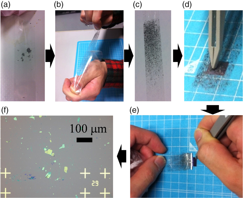
Since the first isolation of monolayer graphene in 2005,16) various kinds of layered crystals are mechanically exfoliated down to atomic layers. The process is very simple: put a crystal on Scotch tape, fold and unfold it ∼10 times, and then transfer the flakes onto a SiO2/Si substrate (Fig. 1). It is essential to use the tape having proper adhesiveness. In general, crystals with strong mechanical strength such as graphite are exfoliated using strongly adhesive tape, while less adhesive is preferable for fragile crystals such as TMDs. Mechanical exfoliation looks primitive, but it is applicable for all sorts of 2D crystals and can provide atomic layers having little defects and high-quality.

Fig. 1. (Color online) Mechanical exfoliation. (a) Put crystals on tape. (b) Fold and unfold it several times. (c) Flakes are scattered on the tape. (d) Put the tape on a SiO2/Si substrate and scrape it gently with tweezers. (e) Remove the tape slowly. (f) Exfoliated flakes are randomly attached on the SiO2/Si substrate.
Download figure:
Standard image High-resolution image2.2. Identification of atomic layers
Crystal flakes of layered materials exfoliated randomly on SiO2/Si substrates are searched and identified under an optical microscope. Although the flakes are as thin as their atomic limits, they can be visible due to the optical interference, and the thickness of atomic layers is identified by the color contrast. Figure 2(a) shows a schematic of the system of graphene on a SiO2/Si substrate. Light incident from the upper side of graphene either goes through or be reflected at the interfaces of air/graphene, graphene/SiO2, and SiO2/Si. These light waves interfere with each other to generate the optical contrast depending on the thickness of the 2D flake and SiO2. Figure 2(b) shows a calculated optical contrast of graphene on SiO2 based on the scheme discussed by Blake et al.17) The ideal SiO2 thickness for graphene is ∼100 and ∼290 nm. For the 290 nm SiO2, the contrast becomes maximal at a wavelength of ∼560 nm [Fig. 2(c)], as represented by optical micrographs of graphene [Figs. 2(d) and 2(e)]. Thus, the use of a green optical filter facilitates to find graphene and identify the number of layers. In contrast, graphene is hardly visible on a 200 nm SiO2 owing to the weak optical contrast in a visible light regime. Besides, the contrast depends on the material. For example, few-layer h-BN, which is hardly visible on 290 nm SiO2, can be identified on ∼85 nm SiO2.18) Further, in the transfer process described later, flakes are exfoliated on a polymer sheet spin-coated on a SiO2/Si substrate. The optical contrast of graphene on a polymer sheet can be calculated similarly to the above [Figs. 2(f)–2(j)].19)

Fig. 2. (Color online) Schematic structure, calculated optical contrast, and optical micrographs of (a)–(e) graphene/SiO2/Si and (f)–(j) graphene/poly(propylene) carbonate (PPC)/SiO2/Si. Even with the insertion of the PPC layer, graphene is visible with the proper thickness of PPC. (Reproduced with permission from Ref. 19).
Download figure:
Standard image High-resolution image2.3. Advanced techniques
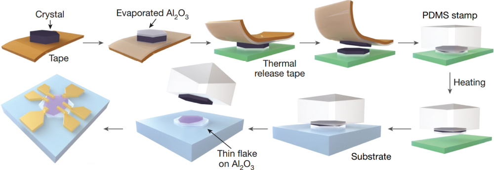
In the exfoliation process, adhesion between the cleavage surface and the substrate is critical. Huang et al.20) reported that the size of exfoliated flakes increased astonishingly by 20–60 times by heating the substrate to 100 °C after attaching the tape onto the substrate. Moreover, mechanical exfoliation can be performed by other than Scotch tape. By directly depositing Al2O3 on a crystal on tape and stripping it off, Deng et al.21) isolated monolayers from Fe3GeTe2 bulk crystals, which was regarded as a material that is difficult to be thinned down to monolayer, and discovered itinerant ferromagnetism in atomically thin Fe3GeTe2 (Fig. 3). This method facilitates the exfoliation of large atomic layers from a wide range of layered crystals.

Fig. 3. (Color online) Exfoliation of Fe3GeTe2 bulk crystals. Al2O3 is deposited onto a crystal on tape, and then the crystal is cleaved by tapes. Thin flakes are obtained on Al2O3. (Reproduced with permission from Ref. 21).
Download figure:
Standard image High-resolution image3. Stacking atomic layers
Fabrication of vdW heterostructures was first demonstrated in 2010. In principle, exfoliated flakes of 2D materials can be assembled in the desired order by vdW force. However, the actual fabrication of heterostructures is not as easy as imagined. Many scientists have devoted considerable effort to devise creative solutions to the vdW assembly and are still searching for ways to improve device qualities.
Transfer methods of atomic layers utilize the adhesive force of transparent polymers to pick and release the flakes. They are divided into two categories: the bottom-up process and the top-down process (Fig. 4). The former is to construct a structure starting from the bottom to the top layers by stacking layers one by one. The latter is to start with the top layer and pick up the following layers by vdW force. In this section, we describe representative bottom-up and top-down transfer methods.
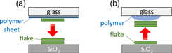
Fig. 4. (Color online) Schematic of the (a) bottom-up and (b) top-down processes of transferring atomic layers.
Download figure:
Standard image High-resolution image3.1. Bottom-up transfer
3.1.1. Water-based polymer transfer
The transfer of atomic layers was first demonstrated by Dean et al.3) They demonstrated a transfer of graphene on h-BN using polymer layers. Graphene on h-BN showed dramatically improved carrier mobility than that in graphene on a SiO2 substrate, testifying that h-BN can be used as an ideal substrate for 2D materials. This is the first vdW heterostructure of 2D materials, which opened up the field of vdW composite materials.
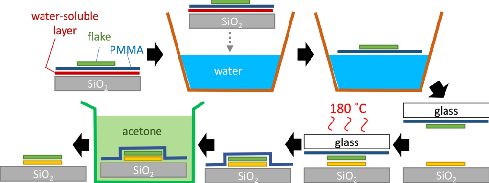
Figure 5 shows a schematic procedure of this water-assisted polymer transfer. First, polymethyl methacrylate (PMMA) and a water-soluble polymer are spin-coated on a SiO2/Si substrate. Flakes are directly exfoliated on the polymer sheet. Even on the polymer sheet, flakes are visible by tuning the thickness of the polymer layer. When immersed in water, the water-soluble layer dissolves and separates the PMMA layer and the substrate. The floating PMMA layer is scooped with a glass slide and then laid onto a target flake under an optical microscope. The top PMMA layer is removed by immersion into acetone, and a layered vdW heterostructure is obtained (Fig. 6).

Fig. 5. (Color online) Water-based polymer transfer. Spin-coat a water-soluble polymer and PMMA on a SiO2/Si substrate and exfoliate flakes on it. Put it into water and scoop the floating flake on PMMA by a glass slide. Align the position of the flake and target flake and bring them into contact.
Download figure:
Standard image High-resolution image
Fig. 6. (Color online) Optical images of (a) graphene and (b) h-BN before transfer and (c) after transfer. Scale bars represent 10 μm. The inset shows electrical contacts. (d) Schematic of the transfer process. (Reproduced with permission from Ref. 3).
Download figure:
Standard image High-resolution image3.1.2. Polymer transfer without using water
The water-based polymer transfer requires dexterous operations of scooping a floating flake and the immersion in water, which can induce wrinkles and adsorption of molecules to the flake. Thus, this method was modified to mechanically peel off the polymer layer from the SiO2/Si substrate. Taychatanapat et al.22) replaced the water-soluble polymer with polyvinyl alcohol (PVA) and fabricated trilayer graphene device on h-BN without immersing it into water.
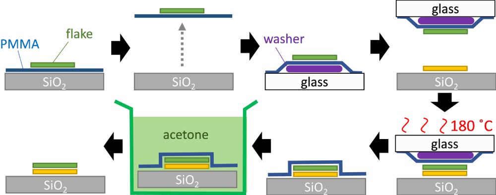
The polymer layer is mechanically peeled off from the substrate using tape (Figs. 7 and 8). Flakes are dropped off by melting the polymer by heat. The PMMA leftover is removed by acetone treatments. This kind of transfer method, which leaves the residual polymer and requires the immersion in organic solvents, is called the "wet-transfer" method.

Fig. 7. (Color online) PMMA/PVA transfer. PMMA/PVA is spin-coated on a SiO2/Si substrate, on which crystal flakes are exfoliated. The polymer layer is mechanically peeled off from the substrate and laid on a supporting washer on a glass slide. After the contact, the substrate is heated up to 180 °C, leaving both the polymer and the flake.
Download figure:
Standard image High-resolution image
Fig. 8. (Color online) The preparation of the PMMA/PVA layer. Tape is attached on every side of the spin-coated PMMA/PVA layer, which is peeled off mechanically. (Reproduced with permission from Ref. 22).
Download figure:
Standard image High-resolution image3.1.3. Dry transfer using PDMS
The wet-transfer inevitably leaves the polymer over the flakes upon melting the polymer at high temperatures, which is difficult to be cleaned up even after hours of acetone immersion. It is preferable not to melt the polymers to reduce the residues on the flakes. This kind of transfer method, which does not require the melting of polymers and succeeding immersion to organic solvents, is called the "dry transfer" method. The dry transfer was first reported by Castellanos-Gomez et al.23) using polydimethylsiloxane (PDMS). They demonstrated a fabrication of MoS2/h-BN heterostructures as well as freely suspended structures of MoS2 and few-layer (∼10 layers) graphene. This method does not require heating of the substrate, which is why it is often used for TMDs, which can be affected by the heat treatment in the air.
Figure 9 shows the process of the PDMS dry transfer. Flakes are directly exfoliated onto a piece of PDMS sheet attached to a glass slide. After the PDMS sheet and a target flake get into contact, the sheet is slowly peeled off, leaving the flakes on the target (Fig. 10). Owing to the viscoelastic nature of PDMS, the peeling speed should be slow to lower the adhesion force between the flake and PDMS.

Fig. 9. (Color online) PDMS transfer. A flake exfoliated on PDMS comes in contact with a target flake at the bottom. The PDMS stamp is slowly peeled off, and the flake is dropped off onto the target flake.
Download figure:
Standard image High-resolution image
Fig. 10. (Color online) MoS2/h-BN heterostructures transferred by PDMS. (Reproduced with permission from Ref. 23).
Download figure:
Standard image High-resolution imageThe PDMS transfer has been widely used as an easy and efficient way to transfer TMDs. On the other hand, this method cannot be used for monolayer graphene and few-layer h-BN. One of the reasons is the difference of transmittance: Thin TMDs can be distinguished on transparent PDMS owing to their moderate values of optical transmittance, whereas graphene and h-BN are hardly visible in the form of few-layers (optical absorbance is ∼2% for monolayer graphene). Therefore, another dry transfer method is required for graphene and h-BN.
3.1.4. Dry transfer using PPC
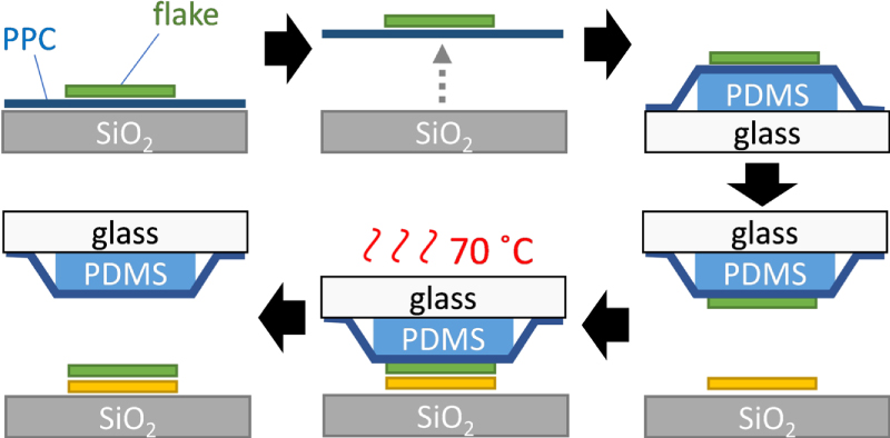
The key point of the successful dry transfer is to realize good adhesion between a transferred flake and a target flake upon their contact. This is achieved by using a piece of PDMS as a supporting layer. Uwanno et al.24) reported such a modified version of the transfer method by combining PMMA with PDMS, increasing the success rate of the dry transfer. Recently, Kinoshita et al.19) have developed another dry transfer method using polypropylene carbonate (PPC), as described below.
As is the same in PMMA/PVA transfer, flakes are exfoliated onto a spin-coated PPC sheet on a SiO2/Si substrate and peeled off (Fig. 11). Then the sheet is laid on a small piece of PDMS, which is pre-treated by oxygen plasma to increase the adhesiveness between the PDMS and PPC. After the flake and the target are brought into contact, the substrate is heated up to 70 °C, which is the glass transition temperature of PPC. Then, the PPC sheet is slowly detached, leaving the flake on the substrate. It does not require any post-immersion in acetone.

Fig. 11. (Color online) PPC dry transfer method. PPC is spin-coated on a SiO2/Si substrate, and flakes are exfoliated onto it. The PPC layer is mechanically detached from the substrate and put onto a small piece of PDMS on a glass slide. The flake on PPC and the target get into contact, and the substrate is heated to 70 °C. PPC is slowly detached from the substrate.
Download figure:
Standard image High-resolution imageThis PPC dry transfer method is applicable for graphene down to one layer and thin h-BN down to three layers by adjusting the thickness of the PPC layer on a Si/SiO2 substrate. The surface of the transferred flakes is clean, confirmed by atomic force microscopy (AFM) topography (Fig. 12). These improved bottom-up transfer methods have an advantage of wide flexibility in device designs, enabling complex structures. Utilizing the PPC method, innovative device structures have been realized, such as graphene devices having local gates25,26) and embedded electrodes in the stack27,28) to maximize the photo-thermoelectric effect.

Fig. 12. (Color online) (a), (b) Optical micrograph, (c), (d) AFM topographic image, and (e), (f) AFM height profiles of (a), (c), (e) monolayer graphene on thick h-BN and (b), (d), (f) three-layer h-BN on thick h-BN. (g) Schematic and (h) optical image of the device of top-contacted h-BN/Gr/h-BN sample fabricated by the PPC method. (Reproduced with permission from Ref. 19).
Download figure:
Standard image High-resolution image3.1.5. Removing polymer residues
In the bottom-up process, atomic layers are inevitably contacted to polymer sheets. Most of the polymer residues can be cleaned up by immersion to organic solvents, though the effect saturates in a few hours.29) AFM or Raman spectrum measurements can identify polymer residues of 1–2 nm thick,29,30) which are not visible under an optical microscope. These residues not only increase the surface roughness and cause bubbles but also degrade the contact resistance of the attached electrodes31) and give rise to chemical doping.29,32,33) The covering layer of polymer residues also accounts for additional emission peaks in optical measurements.29,30,34) To overcome this problem, various attempts have been made to minimize residues. The most popular one is the high-temperature annealing. In a flow of Ar/H2 gas or vacuum at a temperature of 300 °C–350 °C, PMMA is decomposed into smaller molecules.29,30,32) Similarly, PDMS residues can be cleaned up by vacuum annealing.30) The effect of annealing changes with the gas composition. For h-BN, annealing in a flow of Ar/O2 at 500 °C is highly effective in removing both PMMA and adhesive tape residues (Fig. 13).35)

Fig. 13. (Color online) Effect of Ar/O2 annealing on PMMA residues. (a) AFM profile of an h-BN flake with PMMA residues. Raman spectra are acquired at locations indicated with (b) blue and (c) green marks in (a). Residues are effectively cleaned after annealed in Ar/O2 at 500 °C. (Reproduced with permission from Ref. 35).
Download figure:
Standard image High-resolution imageAnother approach is the ozone plasma cleaning of the sample surface. After the ozone cleaning, the contact resistance of graphene is reduced by one-tenth of the value without treatment due to the reduced thickness of PMMA residue on top.31,36) The exposure time should not be too long since the excess ozone exposure would damage graphene and end up increasing contact resistance due to epoxide defects.37) On another front, one can prevent the residues by pre-treatments of polymer sheets. The surface of PDMS sheets can be cleaned up by ozone plasma30) or IPA rinse,38) which dramatically decreases the residues (Fig. 14).

Fig. 14. (Color online) AFM profiles of MoS2 flakes transferred by PDMS (a) without and (b) with the pre-cleaning by ozone irradiation. (Reproduced with permission from Ref. 30).
Download figure:
Standard image High-resolution image3.2. Top-down transfer
In the bottom-up process described so far, atomic layers inevitably contact with polymer layers. While the magnitude of the residue varies depending on the polymer, it is plausible that the contact with polymer has some negative influence on the flakes. In this subsection, we introduce the top-down assembly of vdW heterostructures, which is a way that can avoid such unfavorable contact with polymers.
3.2.1. Pick-up method
Wang et al.39) demonstrated a top-down assembly of graphene devices sandwiched by h-BN flakes by picking up the layers one by one using adhesive polymer stamps. As shown in Fig. 15, a flake on a SiO2/Si substrate, which will be the top layer of the structure, is picked up using an adhesive polymer on a glass slide. This top layer should be a flake with a middle thickness. 20–60 nm thick h-BN is often used for the first flake, which prevents the succeeding flakes from wrinkling. The next flake is then picked up by vdW force at the interface. Therefore, the following flakes avoid direct contact with the polymer stamp (Fig. 16). By repeating this process, vdW heterostructures are assembled on the stamp. Finally, the stack is dropped off onto a substrate at 90–180 °C depending on the polymer. Commonly used stamp polymers are PPC,39) PC,40) and Elvacite.41)

Fig. 15. (Color online) Pick-up transfer using Elvacite. A Polymer stamp on a glass slide and a flake on a substrate are brought into contact, and then the flake is picked up. Repeat this process until the stack is completed. The stack is dropped off onto a substrate by heating it up to 180 °C. Remove the polymer residue by immersing it into chloroform.
Download figure:
Standard image High-resolution image
Fig. 16. (Color online) Graphene sandwiched by h-BN flakes prepared by the pick-up method using PPC. (a) Optical image, (b) AFM image, and (c) high-resolution cross-section annular dark field-scanning transmission electron microscope (ADF-STEM) image. (Reproduced with permission from Ref. 39).
Download figure:
Standard image High-resolution imageBecause the functioning layer (usually graphene or TMDs) are buried in the stack, the electrical contacts are made at the edge of the stack exposed after plasma etching. Throughout the process, the inner layers never contact the polymers and are protected from unfavorable outer environments once assembled. The carrier mobility of graphene devices fabricated by the stamping method can exceed 1 000 000 cm2 V−1 s−1 at low temperatures,40,42) which is now only limited by the size of the device. Most of the state-of-the-art graphene devices were fabricated by this method, including the ones showed the fractional QHE8) and superconductivity.14) Recently, edge contacts to monolayer MoS2 have been studied.43,44) Edge-contacted MoS2 devices showed higher electrical performance than the ones fabricated by other methods.
The electrical contact to the inner layer can be made not only at the edge but also at the surface of the stack. Uwanno et al.45) demonstrated the fabrication of the surface electrical contacts to graphene sandwiched between h-BN layers by selectively etching away the top h-BN.
3.2.2. Tear-and-stack method
One of the recent striking discoveries in graphene research is the emergence of superconductivity in graphene bilayer with a lateral orientation angle θ ∼ 1.05°, which was first reported by Cao et al.14) They fabricated their samples by tearing one graphene sheet using the pick-up process, so-called the tear-and-stack method (Fig. 17), which was first demonstrated by Kim et al.46) First, only one half of a graphene flake is picked up by middle-thick h-BN. The other half is picked up after the SiO2 substrate is rotated by the desired angle. In principle, this tear-and-stack method enables precise control of θ than paralleling the straight edges of two individual flakes. However, the resulting θ can slightly deviate from what is expected. It can be inferred that shear stress is applied to graphene sheets during the tearing process, which slightly shifts the lateral orientation of graphene. To divide thicker flakes, they may be cut before picked up using an AFM tip or plasma etching (Fig. 18).46) As the superconducting behavior in magic-angle twisted bilayer graphene and other θ dependent phenomena could be influenced by a slight shift in θ, a way for the precise alignment of θ in a precision better than 0.1° is strongly demanded.

Fig. 17. (Color online) Tear-and-stack method. A thin flake (graphene) on a SiO2/Si substrate is split at the edge of the h-BN flake upon picked up.
Download figure:
Standard image High-resolution image
Fig. 18. (Color online) (a) Optical image of a bilayer graphene flake sectioned at the point indicated by the arrow using an AFM tip. (b) Optical image of the rotationally aligned double bilayer graphene separated by interlayer h-BN. The dashed lines mark the contours of the two layers. (c) Optical micrograph of the device after metal contact deposition. (Reproduced with permission from Ref. 46).
Download figure:
Standard image High-resolution image3.2.3. Removing bubbles
The universal problem of vdW stacks is bubbles (blisters) that arise between layers. The contents of these bubbles are air, water, and hydrocarbon47) trapped during the stacking process. Hydrocarbon is originated from the polymers used in the transfer, such as PMMA, PDMS, and PC. The size of the bubbles is a few nm-μm in diameter, locating at intervals of 1–20 μm. The height of the bubbles reaches ∼1 μm, which causes the above layer to be strained to wrap up the bubble.48) These bubbles have distortive impacts on device performance in terms of electrical47,49) and optical50) properties.
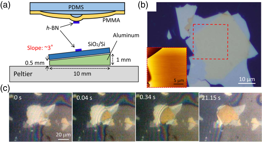
The most conventional attempt to remove bubbles is annealing. At high temperatures, bubbles become movable and either get together to form a bigger one or escape from the edge of the stack. Devices are fabricated using bubble-free regions after annealing. An AFM tip is also useful to mechanically push away the bubbles,38,49,50) while it is difficult to clean up the entire region of a large device. To obtain heterostructures having large bubble-free regions, one should pay close attention during the stacking process. Bubbles are easily trapped at the interface when the speed of approaching the target is too fast. In the pick-up method, the most important is the end of the stacking process, when the bubbles can be pushed away by slowly pushing the stack against the substrate at high temperatures (Fig. 19). With this method, Purdie et al.40) realized a graphene device having a bubble-free area of as large as ∼5000 μm2, which exhibited carrier mobility of ∼1 800 000 cm2 V−1 s−1 at T = 4 K. On another front, one can prevent the incorporation of bubbles by devising the contact angle. Toyoda et al.51) demonstrated the reduction of bubble formation at the interfaces by inclining the bottom substrate. Bubbles can also be reduced in an atmosphere containing less amount of contaminant molecules, such as in a vacuum.52)

Fig. 19. (Color online) (a) Schematic illustration of the inclined substrate and PMMA/PDMS lens. (b) Typical image of the bubble-free transfer of the h-BN/h-BN heterostructure. Inset: the AFM image at the red broken rectangular region. (c) Successive images during the unidirectional transfer using the inclined substrate. (Reproduced with permission from Ref. 51).
Download figure:
Standard image High-resolution image4. Toward automatic robotic fabrication of vdW superlattices
Thus far, we have described fabrication methods of vdW heterostructures, where all of the fabrication processes are conducted manually, just like handcrafts. The accessibility of these fabrication techniques enabled the rapid expansion and progress of 2D materials research all over the world. On the other hand, manual operations take much time and inevitably include unintentional mistakes. Besides, it is difficult to convey the condition of manual processes to other persons. For example, we are routinely instructed to scrape the tape "gently" with tweezers in the mechanical exfoliation, but it is completely unclear how "gently" we should scrape, as it is not a quantitative expression. As a result, the exact process condition is different from person to person and is not so much reproducible.
In this situation, it naturally comes to mind that these problems could be resolved by the "industrial revolution," i.e. automatization of the fabrication process. In this section, we introduce the recent trend in vdW assembly to use robotic apparatus and computational algorithms.
4.1. Determination of flake thickness by image analysis
In general, the thickness of the atomically thin flakes is determined by the color contrast of the flakes. However, the determination with the eyes could be ambiguous as there are multiple factors that influence the flake image including subtle change in SiO2 thickness, illumination light, and the optical microscope used. In most cases, it requires much more time and effort in searching for desirable flakes for a device than in stacking them. Besides, the optical contrast is different among materials. As the number of layered materials is increasing, it takes quite a bit of work to manually correlate the optical contrast and the thickness for each material. Therefore, there is a strong demand for automatization of the searching process to find 2D flakes in a short period.
Recently, an automated searching system has been established by Masubuchi et al.41) In this system, optical images of the flakes on SiO2/Si substrates are processed through an algorithm that extracts the feature quantities of the images (Fig. 20). Based on these extracted features, the region of flakes is identified in the images. This system is capable of searching 10000 graphene monolayers in 8 hours and is integrated into the automated robotic assembly system described in the next subsection.

Fig. 20. (Color online) Workflow of automated searching. An optical RGB image of flakes is converted into HSV images. H: hue, S: saturation, and V: value. Based on these images, the region of the flakes is identified. (Reproduced with permission from Ref. 41).
Download figure:
Standard image High-resolution imageAs an evolved form of this image analysis, one can utilize machine learning to categorize flake images. Since the number of atomic layers is a discrete quantity, it is an ideal platform for the study of machine learning. In a recent work,53) numerous flake images were analyzed to extract feature quantities of Hue, Saturation, and Value, which formed discrete clusters in (H, S, V) space (Fig. 21). Each cluster corresponds to residues and flakes with 1, 2, 3, ... layers thick. This algorithm can classify flake images of 1, 2, 3, and 4-layer graphene with an accuracy of ∼90%.

Fig. 21. (Color online) Plots of H, S, and V of graphene flakes exfoliated on SiO2/Si substrates with SiO2 thickness (a) 290 and (b) 85 nm. The clusters labeled A, B, C, ... correspond to residues and graphene of 1, 2, 3, ... layers- thick. (Reproduced with permission from Ref. 53).
Download figure:
Standard image High-resolution imageFurther forward, deep learning enables the segmentation of various 2D materials.54–57) Through training with many flake images, the neural network develops a skill to identify atomic layers on SiO2/Si substrates. The algorithm based on deep learning is implemented in the automated searching system41) described in Sect. 4.1 and is shown to be robust against the change in image quality and have broad utility than conventional rule-based detection.54)
4.2. Robotic assembly
With the transfer methods described in Sect. 3, one can stack dozens of layers in principle. However, the actual number of manually stacked layers has been limited to ∼10. Manual operations require much time and lack reproducibility. It is highly demanded for further development of vdW composite research to increase the number of layers while decreasing the time needed for fabrication. For a breakthrough of this limitation, a robotic assembly system has been established (Fig. 22). This system includes the whole process of the vdW assembly, from searching to stacking. Flakes on SiO2/Si substrates are searched automatically, and their optical images are stored in a database, which can be accessed upon designing the device structure in CAD software. Then flakes are stacked by the pick-up method using robotic arms and a movable stage, which are remote-controlled on a computer screen. All the robotic apparatus is packed in a glove box in a nitrogen atmosphere. This system demonstrated the fabrication of vdW superlattices of ∼30 layers in less than one day. The automatization of the vdW assembly would be a worldwide trend.

Fig. 22. (Color online) (a) Schematic and (b) photographic image of the robotic assembly system. (c) Optical image of graphene/h-BN vdW superlattice structures fabricated by the system. (Reproduced with permission from Ref. 41).
Download figure:
Standard image High-resolution image
5. Summary and perspective
In this article, we have described the fabrication techniques of atomic layers and vdW heterostructures. Researchers have developed a number of transfer techniques, some of which have been improved over time to have better productivity and fewer residues. Each method has its own strong points. For example, the stamping method is effective in fabricating high-quality devices with simple structures. The PPC method is useful to realize complicated device designs. For TMDs, the PDMS transfer is a fast and convenient way. Therefore, it is essential to employ an appropriate method depending on the purpose. In the future, it is anticipated that advancement in these techniques will enable us to manipulate and assemble the layers in a desired manner by moving, dividing, and folding 2D flakes. This will dramatically expand the flexibility of device designs and realize the free construction of vdW heterostructures like playing with building blocks. Besides, the required time and effort for the vdW assembly will be decreased by the automated stacking and searching of layered materials. These trends of automation of the fabrication process should accelerate the progress in the 2D materials research. Finally, we hope this article will help the readers to understand the basics of vdW assembly and motivate them to try the fabrication by themselves.
Acknowledgments
This work was supported by CREST, Japan Science and Technology Agency (JST) under Grant No. JPMJCR15F3, and by JSPS KAKENHI under Grant Nos. JP19H02542 and JP19H01820.
Biographies

Momoko Onodera received her M.Eng. from Department of Materials Engineering, The University of Tokyo in 2018. She is currently a Ph.D. student under the supervision of Professor Tomoki Machida at Institute of Industrial Science, The University of Tokyo.

Satoru Masubuchi received Ph.D. degrees from Department of Applied Physics, the University of Tokyo in 2010. He was a research associate from 2010, and has been a project lecturer at the Institute of Industrial Science, University of Tokyo since 2016. His current research interest includes quantum transport in 2D materials, deep learning, and robotic fabrication of van der Waals heterostructures.

Rai Moriya received his Ph.D. from Department of Information Processing, Tokyo Institute of Technology, in 2004. From 2004 to 2007, he was a postdoc at IBM Research Division, Almaden Research Center. From 2007 to 2009 he was a Research Staff Member of IBM Research Division, Almaden Research Center. From 2009 to 2017, he was a research associate of Institute of Industrial Science, University of Tokyo. Since 2017, he has been a project lecturer of Institute of Industrial Science, University of Tokyo. His research interests cover physics and applications of two-dimensional materials.

Tomoki Machida received his Ph.D. degree from the University of Tokyo in 1998. He is a professor in the Institute of Industrial Science, University of Tokyo. His current research interests include quantum transport in van der Waals junctions of graphene and 2D materials.