
Abstract
An X-ray standing wave (XSW) is created in the overlap region of two coherent X-ray waves, e.g. by diffraction or reflection. The XSW intensity maxima move, when traversing the range of total reflection, causing strong modulation of the photo-excitation of a particular element or atomic species, recorded by electron or X-ray fluorescence spectroscopy. The XSW technique is a Fourier technique, particularly useful for identifying and structurally characterizing diluted, active species. In simple cases, a single XSW measurement allows characterization with pm resolution. Otherwise, employing several XSW measurements, an image can be created by Fourier inversion allowing one to identify individual sites. The principle, strength and limitations of the XSW technique are reviewed briefly and we focus on three examples for identifying active sites: catalytically active Al in scolecite, magnetically active and counter-active sites of Mn in GaMnAs and sites on the SrTiO3(001) surface active in the splitting of water.
Export citation and abstract BibTeX RIS

Content from this work may be used under the terms of the Creative Commons Attribution 4.0 license. Any further distribution of this work must maintain attribution to the author(s) and the title of the work, journal citation and DOI.
1. Introduction
The X-ray standing wave (XSW) technique1) utilizes X-ray interference in order to lend spatial resolution to powerful X-ray spectroscopy technique such as photoelectron or X-ray fluorescence spectroscopy, the latter case demonstrated already in 19642) by Boris Batterman at Bell Labs. Later, Batteman utilized the interference field created by Bragg reflecting 17.4 keV X-rays by the  = (220) planes of a silicon single crystal for photo-exciting dilute arsenic dopant atoms. Recording As K-fluorescence as a function of the XSW movement, he revealed the substitutional location of the As atoms within in the unit cell of the silicon crystal.3) Since then, there have been numerous applications of the XSW technique (see Ref.1 and references therein). From the beginning, the majority of these dealt with unraveling the structure of highly dilute systems such as dopants and surface adsorbates.4)
The XSW technique, like diffraction, is a Fourier technique, but provides in addition phase sensitive and element specific information. One XSW measurement provides commonly one5) complex Fourier coefficient, i.e. amplitude and phase for the distribution of an elemental species under study. In a short paper, Hertel et al. published 1985 this principle of the XSW analysis6) and in a review of the XSW technique7) we expanded on this principle with focus on surface structure determination.
How to access several Fourier components of the spatial distribution of atomic species had been demonstrated already early in the 1980s.4,8) In case that several obtained Fourier phases and amplitudes have been determined, direct back transformation allows one to construct an image of the spatial distribution of the spectroscopic selected elemental species.9–17)
Every technique has its limitations and it is important to realize that XSW measurements provide structural information on the scale of the achievable wavefield spacings only. These are restricted and this sets firm limits to the accessible length scale, depending on the way the wavefield is created. When using Bragg reflections, the maximum upper limit of the length scale is given by the size of the crystal unit cell.
The XSW method is particularly useful for determining the lattice location of impurity atoms or dopants in a crystal or the position of adsorbates on a surface.7) Thus, these applications have dominated the use of the XSW technique. When using reflection from a synthetic multilayer18) or from an optical surface19) for producing the standing wave, the wavefield spacing and thus the accessible length scale can be several ten nm, allowing, however, only one-dimensional structural analysis.
In principle the movement of the XSW modulates any photon-scattering process and, e.g. Compton20–22) as well as thermal diffuse (i.e. phonon) scattering20,23) have been studied under the influence of XSW excitation. However, structure determination with spatial resolution down to pm relies on photo-excitation. The reason being that the probability for dipolar photo-excitation is proportional to the electric field amplitude precisely at the core of the atom. It is fortunate that dipolar photo-absorption is dominant even in the hard X-ray regime. In fact, even if present, multipole contributions do not impede high structural resolution. They can (and must) properly be taken into account in the XSW analysis.24,25)
The XSW technique distinguishes itself clearly from X-ray diffraction (XRD) techniques that utilize the coherent scattering from the distributed electron cloud. XRD provides high structural resolution in particular for periodic atomic arrangements, but inherently without element specificity. Interpreting measured electron densities or exploiting anomalous dispersion effects provides element specific information, although with some ambiguity. Worthy of note, while the XSW method uses a periodic medium for generating the interference field, periodicity of the system under study is not a prerequisite for its application of the XSW technique.
Besides providing phase sensitive information in Fourier space, the combination of X-ray interference with the elemental and chemical specificity of spectroscopy presents a huge advantage over element indiscriminate elastic scattering employed by diffraction techniques. This is of particular benefit when the species of interest is highly diluted and/or cannot otherwise be discriminated from a surrounding matrix. Owing to spectroscopic filtering, the detection limit is exceedingly low.26)
In the following, we will deal only with planar interference field, created by reflection or diffraction of a plane X-ray wave (and thus distinguish XSW from more general interference/holographic techniques). Furthermore, we will concentrate on the approach of the XSW technique that is most frequently used by far, providing atomic resolution in the pm range, i.e. single crystal XSW, where the XSW is created by Bragg reflection from a crystal lattice. We will discuss XSWs created by multilayer or total external reflection, but only briefly. Both of these variants have found some applications, but both offer neither sub-Å nor 3D resolution.
The XSW technique has meanwhile been reviewed many times, most comprehensively in a 2013 monograph.1) In addition and over the years, several topical reviews of the XSW technique have been published, such as on: surface displacements detection of crystals;27) formation of XSW in distorted crystals;28) Bragg reflection XSW under specular reflection condition;29,30) normal incidence XSW determination of adsorbate structure and Argand diagram analysis;31) theory and applications of XSW in real crystals;32) XSW studies of minerals and mineral surfaces33) and very recently about surface structure determination by XSWs at a free-electron laser.34)
Just for the convenience of the reader we will in Sect. 2 recall some of the bare essential technical requirements and principles of the technique, but only very briefly because of the significant amount of literature available. Fourier imaging by the XSW technique, on which this review concentrates, is a more recent development and has neither been extensively used nor comprehensively reviewed so far.
In Sect. 3, we present and discuss three illustrative examples of XSW analysis. Determining the chemically active aluminum sites in the unit cell of the zeolite scolecite by classical XSW analysis using several reflections is reviewed in Sect. 3.1. Two applications of XSW imaging are described in following Sects. 3.2 and 3.3. Section 3.2 summarizes how the locations of active and counter-active Mn in the unit cell of the dilute magnetic semiconductor GaMnAs were revealed employing ≈20 Fourier components. This number is comparably large for the XSW technique but rather small compared with diffraction techniques. In contrast, Sect. 3.3 is an example of how XSW Fourier imaging, using just two reflection, provides structural information, here about the SrTiO3(001) surface sites that are active in the deprotonation of water.
2. The XSW method
In a nutshell, it is the main principle of the XSW technique to photo-excite atoms by an interference field instead of a transient wave. The generation of an XSW requires firstly a monochromatic and collimated X-ray beam, resembling an X-ray plane wave. Reflection gives rise to a second, coherent plane wave. Overlap of both results in the formation of a standing wave.
Sufficiently collimated and monochromatic X-radiation is nowadays routinely available in the form of monochromatized radiation emitted from undulators installed at third or fourth generation low emittance (see e.g. Ref. 35) synchrotron light source or free-electron laser. Figure 1 shows a schematic experimental setup for XSW measurements at a storage ring. Bragg reflection or total external reflection creates a second coherent plane wave, as schematically shown in Fig. 1 as well. The overlap of the two coherent plane X-ray waves leads to the formation of a planar X-ray interference field, i.e. an XSW. As shown in Fig. 1 for the case of Bragg reflection from the (111) planes of a diamond structure lattice, the equal-intensity planes of the standing wave are periodic with the planes giving rise to the reflection, i.e. with the diffraction planes with spacing  in the shown example. Diffraction planes are not necessarily lattice planes. Shown in Fig. 2 is the case of using (333) diffraction planes, i.e. diffracting from the (111) planes in third order
  as described by the Bragg equation36) by
  Higher order reflection require for the same Bragg angle
  an according shorter wavelength
  , i.e. m-times higher energy. Photon wavelength λ and energy
  are related by
  keV Å. The use of higher order reflection is important for the XSW Fourier imaging technique since it allows one to access higher order Fourier components and thus shorter length scales.
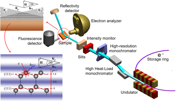
Fig. 1. (Color online) Schematic of typical XSW set-up at a synchrotron radiation source. A double crystal Bragg monochromator selects the appropriate energy from the radiation of a low emittance undulator source. Typically used are liquid nitrogen cooled Si(111) crystals with a bandpass of  Excellent heat conductivity and almost vanishing lattice expansion around 70 K of silicon are important to cope with the high heat load from the insertion device. Depending on the requirements, the bandpass is further reduced by a secondary monochromator. The beam intensity incident on and reflected from the sample is monitored. X-ray fluorescence and/or (photo)electrons from the sample are recorded by energy dispersive detectors. By tuning the angle of incidence, the sample can be "rocked" through the range of (total) reflection. More commonly, when using a multilayer or single crystal, the range of Bragg reflection is traversed at fixed angle by scanning the incident energy. The insets show schematically the formation of the XSW by the incoming and reflected beam with the propagation vectors
  and
and  respectively, related by the Laue equation
  with the diffraction vector
  and the diffraction plane spacing
  the (111) lattice constant in the shown case.
Download figure:
Standard image High-resolution image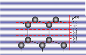
Fig. 2. (Color online) Schematic of an XSW in a diamond structure crystal reflecting from the (111) lattice planes in third order, i.e. using the (333) diffraction planes, which are no physical lattice planes.
Download figure:
Standard image High-resolution imageAt Bragg reflection, the periodicity of the X-ray planar wavefield is in resonance with the crystal lattice. Traversing the reflection range from low to high energy  or glancing angle θ the resonance phase, the phase difference
  between the exciting and reflected X-ray waves, characterized by complex field amplitudes
  and
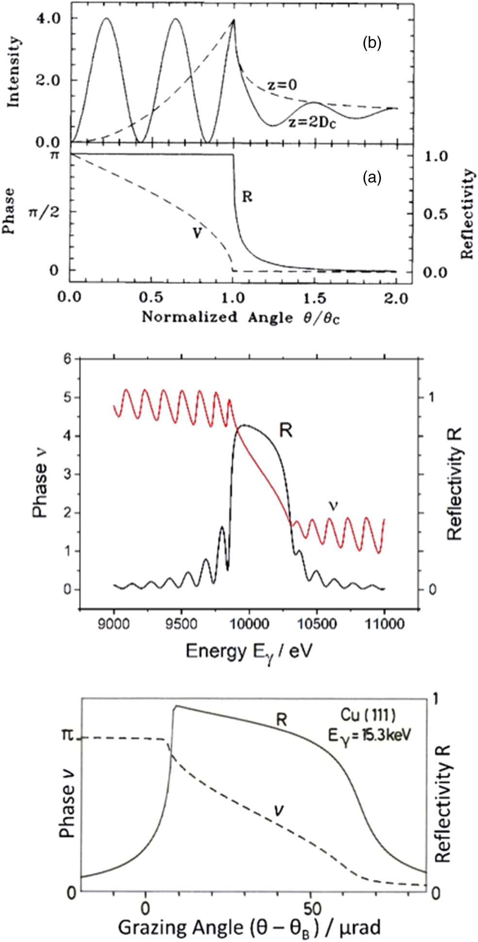
and  respectively, changes by −π (see Fig. 3). The amplitude factor is simply
  with the reflectivity
  and intensities
  Consequently, passing the reflection range, the wavefield planes move inward by half the distance of the diffracting planes.1,37,38) (We assume linearly polarized X-rays and the E-field vectors
  of both waves being collinear. These two conditions simplify the experimental conduct and the data analysis significantly and are commonly employed in XSW experiments.) Reflectivity R and resonance phase
  are shown in Fig. 3 for the cases of reflection from a mirror surface, multilayer and single crystal.

Fig. 3. (Color online) Calculated reflectivity R and phase  for X-ray reflection from a mirror surface (top), a multilayer (middle) and a single crystal (bottom). (Top) Calculated parameters for total reflection of a plane wave from an ideal mirror surface neglecting absorption. (a) Reflectivity R and phase
  of the reflected plane wave. (b) Normalized wavefield intensity at two different heights
  i.e. at the surface and
  above the mirror surface each shown as a function of glancing angle θ with wavelength λ and critical angle
  of total reflection (taken from Ref. 19). [Middle, (c)] Reflectivity R and phase
  of X-rays reflected from a Ru/B4C multilayer with a "lattice constant"
  3.91 nm at Bragg angle
  = 0.947°. Within the range of strong reflection, the resonance phase
  changes by –π but oscillates outside. [Bottom, (d)] Bragg reflection from the (111) diffraction plane of a perfect Cu single crystal.
Download figure:
Standard image High-resolution imageIn the dipolar photo-absorption process, the X-rays are absorbed exactly at the center of atoms and the electrons are emitted without angular momentum. The dipole approximation is largely valid even for hard X-rays, which is the underlying reason of the high spatial resolution of the XSW technique. When scanning the wavefield by traversing the range of Bragg reflection in angle θ or X-ray energy  the concomitantly recorded characteristic electron or X-ray fluorescence emission yield
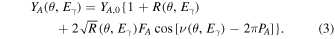
  from an atomic species A is recorded and represents the result on the XSW measurement. The shape of the yield is characteristic of the distribution of species A with respect to diffracting/reflecting plane(s). The yield has the generic functional form
  where
where  is the transition matrix element for the considered photo-excitation process. In absence of multipole contributions this equation simplified to

Here  is the spatial distribution of atom species A and
  is the wavefield intensity at position r, which is a function of θ and/or
  The case of total reflection XSW possesses the peculiarity that not only the position but also the spacing
  of the wavefield is a function of grazing incident angle θ. The intensity of the wavefield has the general form

Employing reflection from a multilayer or a mirror surface, atomic distributions can be analyzed only in one dimension since the diffraction vector  is always normal to the multilayer planes or the mirror surface, respectively. The dot product simplifies to
  where z is the direction parallel to H, i.e. perpendicular to the multilayer planes or the mirror surface. The large spacing of the wavefield does not allow one to obtain the sub-Å resolution, necessary for a detailed analysis of atomic structure. In case of total external reflection, the (variable) wavefield spacing
  allows us to probe large length scales, which requires sufficient longitudinal coherence of the X-rays.39) Multilayer and total reflection XSW have been used for determining wider atomic distributions such as ions in front of electrodes40) and similar applications. In the following, we will not deal with these variants of the XSW technique any longer and concentrate on the most prominent case of Bragg reflection XSW.
When using Bragg reflection for generating the XSW, the result of every measurement of a particular atomic species A on or close to the surface41) is described by the function
The functional form is strictly speaking only correct in the absence of multipole contributions. The two parameters  and
and  represent the
  Fourier components of the distribution
  of atomic species A within the range of the XSW, i.e.
  and
and  where
where ![$[hkl]={\bf{H}}$](https://content.cld.iop.org/journals/1347-4065/58/11/110502/revision2/jjapab4decieqn50.gif) is the diffraction vector characterizing the Bragg reflection used in the XSW measurement. The pre-factor
is the diffraction vector characterizing the Bragg reflection used in the XSW measurement. The pre-factor  is proportional to the density of species A within the range of the interference field. Schematically,
  where
where  is the mean lattice location of the atomic species A. The expression is exact e.g. when the atomic species occupies a unique lattice site.
Quadrupole contributions can become appreciable in differential cross sections, e.g. when detecting photoelectrons within a limited solid angle and the yield function given above needs to be extended. This is meanwhile well understood and can/must be taken into account in the analysis of experimental XSW data.24,25,42)
Fitting the functional form given by Eq. (3) to acquired XSW scan data provides values for the three fitting parameter  Reflectivity R and phase
  are calculated using the structural data of the substrate, used for generating the XSW, using e.g. the dynamical theory of XRD1,37,38) or Parrat's formalism.1,43)
With the help of acquired Fourier components, simple back transformation generates an image

of the distribution of species A within the boundaries of the unit cell of the crystal generating the Bragg reflections. These are limited in number and size with the smallest  determined by largest diffraction plane spacing
  Consequently, length scales beyond the size of the substrate unit cell are not accessible. Such a projected atomic distribution,
  thus naturally exhibits the substrate periodicities, whether the real distribution does or does not have any long-range order. In short, XSW created images of the distribution display the atoms under study confined to or folded into the substrate unit cell.
3. XSW structural analysis and imaging: examples and discussion
3.1. Determining the active aluminum sites in zeolites: scolecite
Zeolites are nanoporous, crystalline aluminosilicate materials that are widely used in industry, e.g. as catalysts and gas separators, as well as our daily life, for example, as adsorbents (e.g. cat litter) or as ion exchangers in laundry detergents.44) The functionality of a zeolite is basically determined by the size and connectivity of the pores and cages, the Si/Al ratio and in particular the placement of the trivalent aluminum atoms at specific sites within the unit cell. The replacement of a tetravalent silicon atom by a trivalent aluminum atom on a so-called lattice T-site creates a local negative charge, serving as binding site for cations. These are then held loosely in the pores and cages of the zeolite allowing them to be easily exchanged. This makes zeolites good cation exchangers, useful in water softening and in the removal of nuclear waste. The Si/Al ratio and the specific location of aluminum in the zeolite framework determine kind and site of the charge-compensating cations, crucially influencing catalytic performance and chemical functionality of the zeolite, but are experimentally not easily accessible [see e.g. Ref. 45 and references therein] e.g. by XRD since the scattering density of Al and Si is rather similar. On the other hand, using XSW, the Al and Si Kα fluorescence signal are clearly distinguishable.
An XSW study of the occupancy of T-sites by Al in scolecite was published in 2008.46) Figure 4 shows the structure of this zeolite. The figure also indicates the three different diffraction planes used for the XSW study, namely the (040), (002) and ( ) reflections. An experimental set-up similar to the one shown in Fig. 1 was used, but with a compound refractive focusing lens47) instead of a post-monochromator. The sample crystal was mounted on a six-circle diffractometer, aligned and scanned in angle through the range of Bragg reflection. Figures 5(a)–5(k) show the yield curves for Si, Al and the Ca cation for the three used reflections and a typical X-ray fluorescence spectrum from the sample [see Fig. 5(l)]. The shapes of the Al and Si curves are clearly different, proving that Si and Al do not occupy the same T-sites. Detailed analysis reveals that none of the T2 sites are occupied by Al. Furthermore, of the four T1 sites only the sites marked by a, b in Fig. 4 are occupied by Al. For more details on the data analysis please consult the original publication.46)
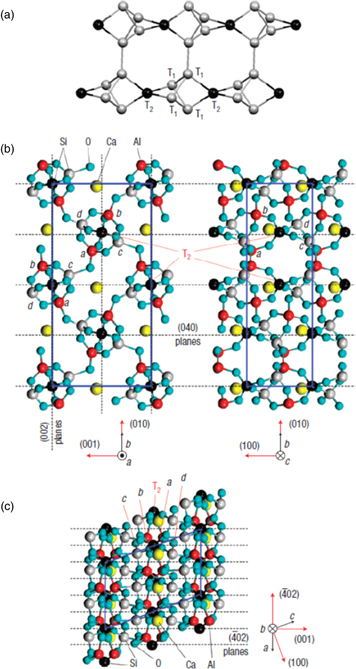
Fig. 4. (Color online) Structure of scolecite. (a) Six of the building units of scolecite, which form natrolite chains. The T-sites (T1, T2) are occupied by aluminum or silicon; oxygen atoms (shown as sticks) join the T-sites. Each building unit contains two types of T-atoms, four T1-atoms and one T2-atom. The T2-atoms link the chain, whereas the T1- and oxygen atoms of neighboring chains form larger pores. In scolecite, the chains are parallel to the crystallographic a axis. (b), (c) Projections of the atomic structure of scolecite along the three axes of the unit cell, marked by the blue rectangles in (b) and parallelogram in (c). The lattice parameters of the monoclinic unit cell are  nm,
nm,  nm,
nm,  nm,
nm,  and
and  There are 20 T-sites per unit cell. The four T1-sites associated with each T2-site are labeled (a)–(d). The dashed lines denote the Bragg planes where coherent position
  for the scolecite (040), (002) and (
 02) reflections. Taken from Ref. 46.
Download figure:
Standard image High-resolution image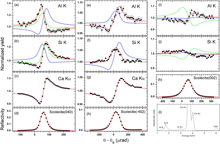
Fig. 5. (Color online) XSW measurements determining Al location in scolecite. X-ray energy: 6 keV. (a) to (k): The XSW yields of K-fluorescence of Al, Si and Ca, normalized by off-Bragg yield [filled circles in (a)–(h)], and reflectivity (filled circles) for three reflections. The red curves are best fits to the data. The blue and green curves represent simulated yields assuming different occupation of the T-sites. (i) Typical fluorescence spectrum from the sample. For more details see Ref. 46.
Download figure:
Standard image High-resolution image3.2. Visualizing manganese in the dilute magnetic semiconductor GaMnAs
Dilute magnetic semiconductors such as Mn doped GaAs48) are under discussion for spintronic applications in device technology. The divalent Mn substitutes trivalent Ga and acts as an acceptor. The holes mediate a ferromagnetic interaction between the local moments of the open d shells in the Mn atoms.48) In the low doping limit, the Curie temperature  increases steadily with Mn concentration. With Mn concentration at around four percent, the Curie temperature
  saturates at a value of around 150 K, still far from the desired room temperature, before decreasing again. The decrease in
  was suspected to be caused by Mn occupying interstitial sites, thereby acting as donor, compensating the hole doping and suppressing p-type conductivity. Direct proof for the validity of this mechanism was missing, stimulating an XSW investigation.16)
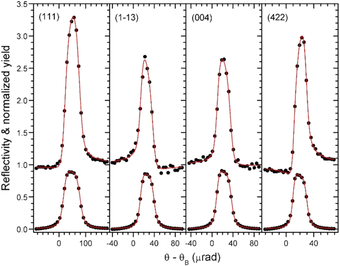
Low temperature molecular beam epitaxy49) was used to grow 23 nm Ga1−xMnxAs thin film with x = 0.048 on a GaAs buffer layer on GaAs(001). The wafer was cleaved and two of the pieces were (i) annealed at 150 °C in air and (ii) hydrogenated in a hydrogen plasma. An as-grown and the two post-growth treated samples were investigated by the XSW technique at a insertion device beamline50) (see Fig. 1) using an excitation energy of 10 keV, i.e. 367 eV below the Ga K-edge, and a high resolution Si(555) post-monochromator. With the samples mounted on a six-circle kappa-diffractometer 18 non-equivalent GaAs reflections were scanned in angle for each specimen while recording the fluorescence from the sample. An X-ray fluorescence spectrum is shown in Fig. 6. and four representative of the 18 XSW scans of the Mn K-fluorescence intensity in Fig. 7. Making use of the symmetry of the GaAs crystal unit cell, the 18 non-symmetry-equivalent reflections provide 50 Fourier components. Using Eq. (4), [Figs. 8(a)–8(c)] is produced, showing the reconstructed images of the Mn location  in the GaAs unit cell for the three investigated samples. The resolution of the image is ≈0.09 nm, consistent with the XSW plane spacing of the highest order reflection used (
 = 0.109 nm). Figure 9(g) shows a ball-and-stick model of GaAs. Comparison with Figs. 9(a)–9(c) reveals that in all three cases (the majority of) Mn substitutes Ga. [Slight upward displacements is attributed to the c lattice constants of the (Ga,Mn)As layers being slightly larger than for the GaAs substrate.]
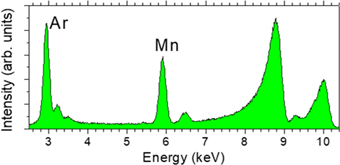
Fig. 6. (Color online) X-ray fluorescence spectrum from a GaAs sample in air with a 23 nm epilayer doped with 4.8% Mn. Excitation energy 10 keV. Argon fluorescence is excited by the beam passing through air. The peaks at around 9 and 10 keV are electronic X-ray Raman scattering from Ga in the sample.
Download figure:
Standard image High-resolution image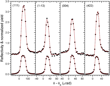
Fig. 7. (Color online) XSW results for four of the 18 used non-symmetry-equivalent GaAs reflections. Symbols are data and red lines are fits to the data. The lower curves are the reflectivity data and the upper curves are Mn X-ray fluorescence data. (Taken from Ref. 16.)
Download figure:
Standard image High-resolution image
Fig. 8. (Color online) (a)–(c) Images of Mn in GaMnAs reconstructed from the 50 Fourier components provided by the XSW measurements of the 4.8% Mn in 23 nm thick GaMnAs films, (a) hydrogenated, (b) as-grown and (c) annealed. (d)–(f) Images created by subtracting the contribution of the Mn on the Ga sites from images (a)–(c), which enhances the residual contributions from the Mn occupying Ga (GaI) and As (AsI) interstitial sites. (g) and (h) Ball and stick model showing the positions of Ga, As (g) and the As- and Ga-interstitial sites (h) in the cubic GaAs unit cell with  nm (taken from Ref. 16). For more details, see text.
Download figure:
Standard image High-resolution image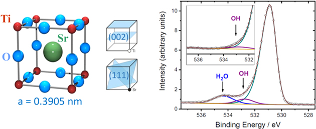
Fig. 9. (Color online) Left: The cubic STO unit cell. There are four symmetry-equivalent (111) diffraction planes. The (002) planes are alternatingly occupied by TiO2 and SrO. Two representations of the STO unit cell are commonly used, either, with Sr at the center or Ti at the center. Right: X-ray PES spectrum from the water dosed STO(001) surface at low temperature displaying three components of the O 1s peak with the largest one originating from the oxygen of the STO bulk. The inset spectrum at room temperature reveals 0.25 Ml OH are stable. Excitation energy  keV (from Ref. 61).
Download figure:
Standard image High-resolution imageIn addition to the intensity at the Ga-substitutional site, there are eight weaker spots at the locations of the Ga interstitial and As sites [see Fig. 9(h)]. They are more clearly visible in Figs. 9 (d)–9(f) where the contribution from the Mn Ga-substitutional site are removed from the images in Figs. 9(a)–9(c). These three edited images clearly reveal that Mn occupies, depending on the treatment, Ga and As interstitial sites, which are schematically shown in Fig. 9(h). Least square fitting the Fourier components of the Mn distribution function  to the experimental
  reveals the Mn distribution on the three sites in the GaAs host lattice with 0.04% accuracy. The detailed description of the analysis is beyond the scope of this review and we refer to the original publication.16)
3.3. Water decomposition on SrTiO3(001)
An important early development was the combination of the XSW technique with photoelectron spectroscopy (PES) 40 years ago, in the late 1970s by Kikuta and Takahashi.51,52) By employing PES, the technique is extended beyond element specific investigations and chemical species can be identified owing to the "chemical shift"53,54) in the photoelectron spectra. Structure of the components with different binding energies can be analyzed individually as we pointed out in our 1993 surface science report7) and which was demonstrated shortly afterwards.55,56) This powerful application of the XSW technique has become meanwhile very popular in surface science and was employed very recently to study the decomposition of water.
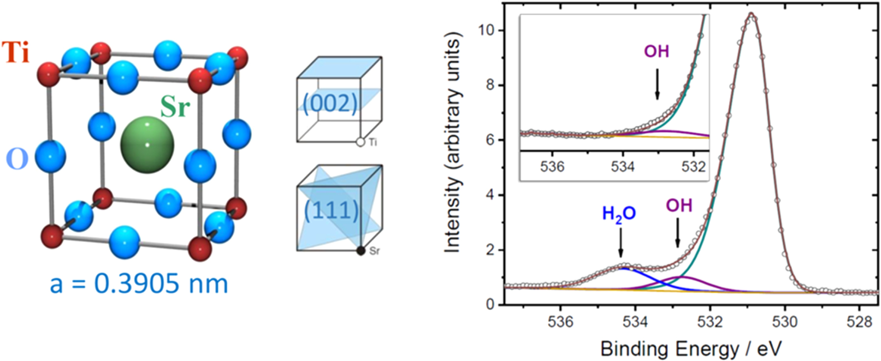
Fuel production from water and sunlight by photo electrochemistry using catalytically active semiconductors may represent a way to satisfy future energy needs. The principle feasibility was demonstrated by Fujishima and Honda in 197257) by the electrochemical photolysis of water at a TiO2 electrode. The same was demonstrated for the cubic (a = 3.905 Å) perovskite SrTiO3 (STO) (see Fig. 10), a semiconductor with a wide, 3.1 eV band gap.58,59) STO becomes n-type conducting (and superconducting60)) via doping, e.g. by oxygen vacancies or Nb5+ substituting for Ti4+. Very recently, the adsorption and deprotonation of water was investigated by the XSW technique combined with PES dosing water on the Ti-oxide terminated STO(001) surface at low temperature in ultra-high vacuum (UHV).61)
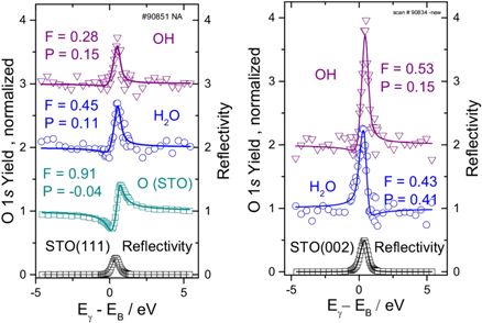
Fig. 10. (Color online) XSW scans at a Bragg angle close to 90° around the STO(111) and STO(002) reflection at 2.76 and 3.18 keV, respectively. Sample temperature 200 K. Symbols are data and lines are fits to the data.61)
Download figure:
Standard image High-resolution imageFigure 10 shows a photoelectron spectrum around the O 1s peak, recorded following deposition of about one monolayer (ML) water at low temperature. The O 1s photoelectron peak has three components. The largest one, at a binding energy of  = 530.8 eV, originates from the oxygen atoms in the bulk of STO. The other two components at
  = 534.3 eV and
  = 532.7 eV arise from oxygen belonging to water and OH, i.e. deprotonated H2O, respectively. Obviously, the water is not stable on the STO(001) surface.
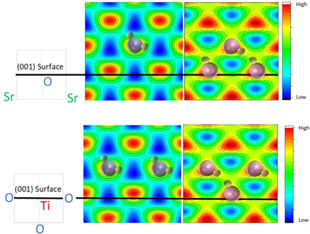
Two XSW scans, using the STO 111 and 002 reflection close to 90° Bragg angle are shown in Fig. 10. The results of the 002 and the 111 reflections provide 1 + 4 symmetry-equivalent Fourier components that are used to construct the images in Fig. 11 of the oxygen positions of water and hydroxyl. Water adsorbs above a surface titanium atom, roughly where oxygen would be located in a continuation of the bulk lattice.61) Even at 200 K, the H2O molecule deprotonates rapidly and the liberated hydrogen atom attaches to a neighboring oxygen surface atom, pulling it few ten pm out of the surface plane,61,62) as shown schematically in Fig. 11 on the right side. Water and hydroxyls are unstable at temperatures above 200 K and desorb rapidly, except for 0.25 Ml OH that is tightly bound to the surface, as the inset in the spectrum of Fig. 9 shows. Whether the reaction products OH and H desorb individually or recombine and desorb as water is still an unsolved question.
Fig. 11. (Color online) Contour plots of the Fourier transform images of the oxygen atom of water (left), and OH (right) reconstructed using the  and
and  values from the (111) and (002) data shown in Fig. STO-2. A single XSW (111) result provides four symmetry-equivalent components because of the high symmetry of the cubic STO crystal. Thus, the images were constructed using five Fourier components. On the scale bar, "High" and "Low" means high and low oxygen atomic density. Water and OH molecules are indicated only schematically; the orientation and position of hydrogen is hypothetical. Top images: Atomic density in the SrO (010) mirror plane. Bottom images: Atomic density in the TiO2 (010) mirror plane. Schematic on the left indicates the respective cut and the corresponding position of Sr, O and Ti atoms in the bulk unit cell (with Ti at the center) indicated by dashed square on the left; black lines indicate the crystal surface for an ideal bulk-terminated crystal. The constructed images reflect the periodicity of the STO lattice because of the periodicity of the standing wave (Fourier components
  are not accessible). Realistic bond-length dictates the position of water, residing above Ti where it deprotonates with the liberated H attaching to surface oxygen.61)
Download figure:
Standard image High-resolution image
3.4. Discussion
Over the last fifty years or so, the XSW technique has provided valuable contributions to numerous problems in condensed matter physics mostly concerning structure on the atomic level. The method is particularly useful for the investigation of dilute systems, determining lattice-locations of sparsely distributed active species that are important or crucial for electronic, magnetic or chemical properties of the material. We provided here three typical examples: unraveling the location of the active aluminum sites in scolecite, resolving the distribution of Mn dopants in GaAs and determining the adsorbate sites initiating the deprotonation of water on STO.
The investigation of scolecite also demonstrates that XSW analysis can deal with relatively complex substrate crystal structures. Furthermore, of the investigated small (natural) scolecite crystal, though comparably large (≈5 × 0.5 mm2) for a zeolite crystal, only a sub-mm sub-grain could be used for the XSW analysis.46) Zeolites of practical or industrial use are powders with much smaller, μm sized crystals. That XSW measurements with atomic resolution are possible on such a microscopic scale had been demonstrated 2002 with the XSW investigation of a GaAlAs delta layer.63) Coined XSW microscopy, XSW formation and analysis was performed on a μm scale. A different approach for obtaining near-atomic resolution on a microscopic scale using multilayer XSW and full-field X-ray fluorescence imaging was published very recently.64)
In the case of Mn in GaAs, three different Mn species (Ga-substitutional, Ga-interstitial and As-interstitial) contributed to the XSW signals, clearly identified by constructing images from a large number of reflection. In many cases, using numerous reflections for creating an image is not necessary, because the species under study occupies one specific lattice site. When the coherent fraction for a  reflection is (close to) unity, i.e. the amplitude of one Fourier component is overwhelming, the coherent position, i.e. the phase of the Fourier component, directly provides the real space information along the spatial coordinate along
 ![$\left[hkl\right].$](https://content.cld.iop.org/journals/1347-4065/58/11/110502/revision2/jjapab4decieqn83.gif) In case of a single adsorption/lattice site, two or three measurements are sufficient to pinpoint the lattice position.8) However, the use of multiple reflections is indispensable in cases where atomic species that spectroscopy cannot distinguish occupy different, inequivalent sites such as in the case of Mn in GaAs, where single XSW measurements give coherent fractions significantly smaller than unity. The image produced by back transformation allows one to identify model-independently multiple sites and the following analysis by data fitting and refinement provides accurate structural data. Scanning the necessary large number of Bragg reflections is straightforward at an insertion device beamline equipped with a six-circle diffractometer. Employing higher order reflections also requires a low emittance X-ray beam of sufficiently high energy such as it was realized in case of Mn doped GaAs by using a Si(555) post-monochromator.50)
In case of a single adsorption/lattice site, two or three measurements are sufficient to pinpoint the lattice position.8) However, the use of multiple reflections is indispensable in cases where atomic species that spectroscopy cannot distinguish occupy different, inequivalent sites such as in the case of Mn in GaAs, where single XSW measurements give coherent fractions significantly smaller than unity. The image produced by back transformation allows one to identify model-independently multiple sites and the following analysis by data fitting and refinement provides accurate structural data. Scanning the necessary large number of Bragg reflections is straightforward at an insertion device beamline equipped with a six-circle diffractometer. Employing higher order reflections also requires a low emittance X-ray beam of sufficiently high energy such as it was realized in case of Mn doped GaAs by using a Si(555) post-monochromator.50)
The analysis of the reaction of water on STO(001) is a good example for the power of the XSW technique when combined with PES by clearly distinguishing three different oxide species, isolating the oxygen 1s signal of oxygen in STO from OH and H2O and determining the surface location of the latter two. The O 1s signal from STO provided additional information about the STO(001) surface structure.61) Because of the high symmetry of the cubic STO substrate surface with two mirror planes, just two reflections were enough to construct images of the oxygen of OH and H2O on STO(001). However, the constructed images also demonstrate possible pitfalls in case of insufficient data because of limited Fourier coefficients. Firstly, the seeming in-plane periodicity of the images is artificial. XSW imaging does not provide information beyond the size of the substrate unit cell. Furthermore, normal to the surface, the images show the same pattern in the STO and TiO2 plane. The data do not allow one to distinguish whether the oxygen (of OH and H2O) resides slightly above the STO or TiO2 or in both diffraction planes because of the  /2 periodicity of the used (002) diffraction planes (see Fig. 9). Detailed analysis reveals that the hydroxyls are in fact occupying two positions on the surface as shown in Fig. 11, whereas the oxygen of the water molecules occupies as shown only one of the two sites.61) A larger range of XSW measurements or just one additional employing the STO(001) reflection could have remove this ambiguity immediately. The STO(001) reflection is unfortunately rather weak, because the TiO2 and SrO planes possess about the same electron density and almost the cancel each other.
Because of imperfect STO crystals, the study was performed in backscattering geometry,1,65,66) using Bragg reflections close to 90°. In this case, the energy  is dictated by
  the used diffraction plane spacing. Thus, back-reflection XSW measurements, typically performed by scanning the energy
  a small range
  around the Bragg energy
  necessarily need tunable synchrotron X-rays. Back-reflection XSW in combination with PES is presently the most popular application of the XSW technique in particular for analyzing adsorbate structures for surface science. In case of the STO(001) reflection, the back-reflection energy of ≈1.6 keV is not accessible at many synchrotron radiation beamlines.
In the context of surface studies, it is interesting to note that the first XSW application by Cowan et al. in 198067) was an in situ investigation of a solid/liquid interface, Br adsorption on a Si(110) surface from a methanol solution. At that time, the XSW technique had not been adapted to UHV studies. Since then, other in situ XSW investigations have provided unique information about solid/liquid, especially solid/electrolyte interfaces using Bragg reflection XSW68–70) and total reflection XSW40) combined with X-ray fluorescence, and lately using multilayer reflection XSW combined with near ambient pressure PES.71) Besides the enabling the analysis of surface adsorbate structures, the XSW technique revealed details of the interface structure of thin films (see e.g. Ref.72–75) and determined with 10−5 precision minute difference in lattice constant caused by the isotopic composition of crystalline films.76,77)
4. Conclusions and outlook
Without the application of synchrotron radiation, XSW measurements are tedious at best, but for the most interesting applications simply impossible, as for our three examples. At synchrotron radiation sources, the XSW technique can advantageously be combined with other techniques, also only enabled by the properties of synchrotron radiation.
In 2001, Kim and Kortright combined X-ray absorption spectroscopy and X-ray dichroism with XSW,78) Gupta et al. combined it with absorption fine structure79) and very recently Lin et al. excited (resonant) emission spectroscopy80) with the help of a XSW. In this way, complimentary structural information was added to all these techniques.
Another fascinating application of the XSW technique is the analysis of electronic structure. In the dipole approximation of the photo-absorption process, which is largely valid even for valence electrons, the photoelectron emission probability is proportional to the strength of the E-field at the center of the atom. This allows analysis of the electronic real space structure in terms of de-convoluting the valence band (VB) into the contributions from individual atomic sites (see e.g. Ref. 81–83). VB XSW is complementary to resonant photoelectron spectroscopy, since the latter is element specific, while the VB XSW technique is site specific. This was used recently in unraveling the specific VB contributions of the two different Cu species in the unit cell of the YBCO superconductor,83) i.e. gaining information on which of the two Cu species is most relevant/active in forming the superconducting condensate. VB XSW has meanwhile been further extended by combining it with angular resolved PES.84)
The wavefields used for the XSW technique are until now planar and periodic, solely produced by diffraction or reflection from substrates, which necessarily represent a part of the system under study. With the increasing degree of coherence of X-rays from synchrotron sources, interference fields can be created by other means. Tailored beam-splitters can generate XSWs of desired shapes and patterns and it is conceivable that technical advances will allow us to manipulate such XSWs with nm resolution or better. This may open the way to ultrahigh-resolution X-ray spectroscopy/microscopy, similar to the concept used nowadays in optical super-resolution microscopy.85)
Biographies

Born in Germany, Jörg Zegenhagen received his Ph.D. from University Hamburg in 1984, followed by five years in the US as postdoc at SUNY Albany 1984–1986 and subsequently member of staff at AT&T Bell Labs, Murray Hill. He returned to Europe, leading a group at the Max-Planck-Institute-FKF in Stuttgart from 1989–99 and then at the European Synchrotron Radiation Facility in Grenoble. Since 2013, he is the Physical Science Experimental Coordinator at Diamond Light Source Ltd., UK. J. Z. lectured in Germany (Habilitation University Dortmund 1993) and France and received an Honorary Professorship from Amity University, Noida Campus, India. He has (co)authored around 300 publications and edited several books and special journal issues. J. Z. is fellow of the American Physical Society and member of several other professional societies. His research focusses on investigating surfaces and interfaces using synchrotron X-ray scattering, spectroscopy and complementary techniques.