
Abstract
We have shown that the structural and compositional properties of semiconductor interfaces fabricated by surface activated bonding (SAB) would be modified during focused ion beam (FIB) processes operated at room temperature (RT), especially for wide band-gap materials, and such a modification can be suppressed by FIB processes operated at lower temperatures. During FIB processes operated at RT, SAB-fabricated Si/Si and GaAs/GaAs interfaces are amorphized along the interfaces, even at the internal locations deeper than the penetration depth of the FIB, and the impurity distribution across the interfaces is modified. This phenomenon is presumably due to the atomic diffusion assisted by the point defects that are introduced by FIB irradiation. By using FIB processes operated at −150 °C, the FIB-induced atomic diffusion would be ignored for Si/Si interfaces. Meanwhile, the diffusion would be still effective for GaAs/GaAs interfaces, presumably due to the effects of recombination-enhanced defect motion under FIB irradiation.
Export citation and abstract BibTeX RIS

Content from this work may be used under the terms of the Creative Commons Attribution 4.0 license. Any further distribution of this work must maintain attribution to the author(s) and the title of the work, journal citation and DOI.
1. Introduction
Surface-activated bonding (SAB),1) in which surfaces of substrates are activated at low temperatures before bonding by creating dangling bonds under a bombardment of energetic particles in a high vacuum, is a promising method to fabricate tough and steep hetero-interfaces at low cost. SAB does not require high-temperature annealing to obtain sufficient bonding strength, unlike the other direct bonding methods such as hydrophilic, hydrophobic and plasma-assisted bonding. This low-temperature bonding would not induce thermal damage and apparent intermixture across the interfaces. Also, SAB enables us to fabricate any hetero-interfaces free from structural defects such as dislocations and cracks, even for the bonding of dissimilar materials with different crystal structures and lattice constants, unlike epitaxial growth methods. Recently, SAB is applied to the next-generation semiconductors such as diamond,2) SiC,3–6) and GaN,7–9) as well as to the basic semiconductors such as Si and GaAs,10–13) towards low-resistance semiconductor-to-semiconductor hetero-interfaces free from adhesive intermediate layers. Functional devices with hybrid structures, such as high-power semiconductor lasers with a low interface thermal resistance4) and high-efficiency multi-junction solar cells with a low interface electrical resistance,14,15) are so far demonstrated with this direct bonding method.
For the practical use of semiconductor hetero-interfaces fabricated by SAB, we need to optimize the interface resistance, determined by the atomistic structure of the interfaces, by controlling SAB conditions. Therefore, the atomic arrangement and composition around the interfaces have been examined by cross-sectional transmission electron microscopy (X-TEM). According to the previous X-TEM data, obtained using X-TEM specimens fabricated with energetic ions such as focused ion beam (FIB), an intermediate layer would be formed along the interfaces in SAB processes. Amorphous-like layers are frequently observed in many as-bonded interfaces,2–4,8,10–12) but no amorphous-like layer is also reported in some as-bonded and annealed interfaces.5,10,12,16,17) Recently, no amorphous-like layer is observed at as-bonded GaAs/GaAs homo-interfaces, in which an amorphous-like layer has been so far reported,11) by using X-TEM specimens fabricated by chemical mechanical polishing (CMP).18) This conflicting results would be explained with two possible models; (1) amorphous-like layers can be formed during SAB processes, due to the irradiation of energetic atoms depending on the SAB conditions,11) and (2) they can be formed by the irradiation of energetic ions during milling processes, via the introduction of interface defects as observed in ion milling processes.18,19) In general, except by ion milling techniques, it is rather difficult to fabricate X-TEM specimens of hetero-interfaces in which the bonding materials are different in the etching rate. Therefore, in order to discuss the realistic structure and composition around SAB-fabricated hetero-interfaces, we need to understand the impact of ion milling on the structural and compositional analyses of the interfaces. As a preliminary result, we have found that impurity distribution at an interface can be modified during a conventional FIB process at room temperature (RT).19) In the present work, we have therefore examined in detail structural and compositional modifications at different kind of SAB-fabricated interfaces depending on the FIB process operated at different temperatures. We have shown that the modifications would be suppressed at low-temperature processes.
2. Experimental methods
Homo-interfaces of Si/Si and GaAs/GaAs were fabricated by SAB at RT, with the rectangular substrates with {110} edges of B-doped (100) p-Si (with a carrier concentration of 2 × 1014 cm−3) and Si-doped (100) n-GaAs (2 × 1016 cm−3). A pair of the substrates were set in a high vacuum below 5 × 10⁻⁵ Pa so that their edges are almost parallel, and they were activated with an argon (Ar) fast atom beam (with a current of 1.8 mA at an applied voltage of approximately 2.0 kV) for 180 s. Immediately after the activation process, they were pressed for 60 s at 10 MPa.18) In order to examine the distribution of impurity atoms that might be introduced during SAB processes, some amount of iron (Fe) atoms were intentionally introduced by the irradiation of Ar atoms on the susceptors simultaneously with the substrates, during the surface activation process.
X-TEM specimens with an interface were prepared by using a FIB system (FEI, Helios NanoLab600i) with 2–30 kV Ga ions,20) with a cold stage customized for the FIB system (IZUMI-TECH, IZU-TSCS004) (Fig. 1). First of all, a bonded substrates with an interface was cleaved parallel to a {110} edge. Large {1–10} plates with the interface, about 10 × 10 × 2 μm3 in size, were cut from the cleaved surface, and they were then mounted on a Cu grid, of which the thermal resistance was fairly low, with a conventional FIB process operated at RT (as the schematic in Fig. 1). They were then thinned with the FIB processes operated at RT or −150 °C, with the FIB condition summarized in Table I, so that their thickness was less than about 100 nm. During the FIB processes, specimens were irradiated with Ga ions with the incident direction schematically shown in Fig. 1. Therefore, the penetration depth of Ga ions from the specimen surfaces would be a few nm for 2 kV Ga ions, and a few tenth nm even for 30 kV Ga ions.21) Even though thin amorphous layers, about a few nm thick, would remain on the irradiated surfaces after the FIB processes, we did not remove the layers by low-energy Ar ion milling. For comparison, X-TEM specimens with an interface free from irradiation damage were also prepared only by CMP.22,23) During the CMP processes, point defects and extended defects would not be introduced in the specimens.22) Atomistic structure of the interfaces was examined by high-angle annular dark-field (HAADF) and energy dispersive X-ray spectroscopy (EDX) analyses under STEM with a JEOL JEM-ARM200F analytical microscope. In order to examine the internal locations much deeper than the penetration depth of Ga ions, we used the specimens more than about 50 nm in thickness.
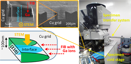
Fig. 1. (Color online) Experimental setup for the irradiation of Ga ions in the FIB system equipped with a cold stage. The inset indicates the schematic view of the irradiation direction.
Download figure:
Standard image High-resolution imageTable I. Irradiation condition of Ga ions for FIB milling.
| Procedure | Acceleration voltage | Incident angle | Beam current | Process time |
|---|---|---|---|---|
| 1 | 30 kV | ±0.8° | ∼0.5 nA | ∼120 s |
| 2 | 30 kV | ±0.8° | ∼0.1 nA | ∼60 s |
| 3 | 8 kV | ±1.5° | ∼0.02 nA | ∼60 s |
| 4 | 2 kV | ±3.0° | ∼0.02 nA | ∼30 s |
3. Results and discussion
3.1. Results
3.1.1. SAB-fabricated Si/Si homo-interfaces
Figure 2(a) shows a HAADF-STEM image of a SAB-fabricated Si/Si homo-interface in X-STEM specimens fabricated with the FIB process operated at RT. No lattice fringe is observed along the interface, indicating that an amorphous layer would exist at the interface, as previously reported.10,12,18) The thickness of the amorphous layer is estimated to be 6 nm. Fe atoms introduced during the surface activation process can be observed as a white band along the interface. The yellow graph in the figure indicates an intensity profile of X-rays due to Fe atoms, that would be proportional to the density profile of Fe atoms, across the interface. The full-width at half-maximum (FWHM) of the Fe profile ranges from 3.4 to 3.7 nm, depending on the analyzed locations.
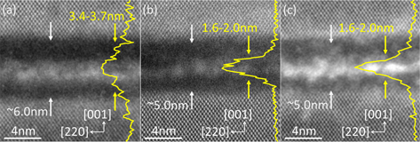
Fig. 2. (Color online) HAADF-STEM image of a SAB-fabricated Si/Si homo-interface taken with a X-STEM specimen; fabricated by FIB milling operated at (a) RT or (b) −150 °C, or (c) fabricated by CMP. The yellow graph inserted in each figure indicates an intensity profile of X-rays due to Fe atoms across the interface. The intensity in each figure increases from right to left.
Download figure:
Standard image High-resolution imageThe same interface as in Fig. 2(a) is examined with the X-STEM specimens fabricated with the FIB process operated at −150 °C. As shown in Fig. 2(b), an amorphous layer is also observed along the interface, but the thickness is reduced by about 1 nm. Moreover, the FWHM of the Fe profile across the interface is also reduced; the FWHM is in the range of 1.6–2.0 nm, as seen in the yellow graph in Fig. 2(b). The estimated thickness and FWHM are the same as those in X-STEM specimens fabricated by CMP [Fig. 2(c)]. This result indicates that, the SAB-fabricated Si/Si interface is amorphized and the impurity distribution around the interface is modified during the FIB process operated at RT, while the structural and compositional modification would be ignored during the FIB process operated at −150 °C.
3.1.2. SAB-fabricated GaAs/GaAs homo-interfaces
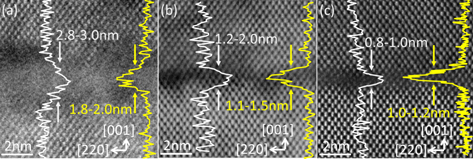
Figure 3(a) shows a HAADF-STEM image of a SAB-fabricated GaAs/GaAs homo-interface in X-STEM specimens fabricated with the similar FIB process as in Fig. 2(a). We can observe an amorphous layer along the interface. The thickness of the amorphous layer is in the range of 2–4 nm, and similar thickness is reported for the similar SAB condition.11) Even though Fe impurities are unclear in the image, EDX reveals that they exist along the interfaces, as seen in the yellow graph in the figure. The FWHM of the Fe profile is in the range of 1.8–2.0 nm. This range is fairly narrower in comparison with the Si/Si interface shown in Fig. 2(a). EDX also reveals an As deficiency along the interface, as reported.18,24) As seen in the white graph in the figure, the intensity of X-rays due to As atoms is decreased across the interface, and the FWHM of the As-deficiency profile is in the range of 2.8–3.0 nm.
Fig. 3. (Color online) HAADF-STEM image of a SAB-fabricated GaAs/GaAs homo-interface taken with a X-STEM specimen; fabricated by FIB milling operated at (a) RT or (b) −150 °C, or (c) fabricated by CMP. The yellow and white graphs inserted in each figure indicate intensity profiles of X-rays due to Fe and As atoms, respectively, across the interface. The intensity in each figure increases from right to left.
Download figure:
Standard image High-resolution image
Interestingly, as shown in Fig. 3(b), no amorphous layer is observed at the same interface in the X-STEM specimens fabricated with the FIB process operated at −150 °C. In the HAADF-STEM image, lattice fringes arrange coherently across the interface, and only a dark band, due to As vacancies,18,24) is observed along the interface. Similar data can be obtained in the damage-free X-STEM specimens fabricated by CMP [Fig. 3(c)]. The GaAs/GaAs interface is, therefore, amorphized during the FIB process operated at RT, while the amorphization can be ignored during the FIB process operated at −150 °C, like the Si/Si interface shown in Fig. 2. Meanwhile, even though the FWHM of the Fe profile across the interface is reduced by lowering the operation temperature [the yellow graph in Fig. 3(b)], the estimated range of 1.1–1.5 nm is still wider in comparison with the damage-free X-STEM specimens fabricated by CMP, with the FWHM of 1.0–1.2 nm [the yellow graph in Fig. 3(c)]. Similarly, the FWHM of the As-deficiency profile across the interface is reduced to the range of 1.5–2.6 nm [the white graph in Fig. 3(b)], but it is wider than the FWHM of 1.3–1.8 nm in the damage-free X-STEM specimens [the white graph in Fig. 3(c)]. Therefore, the composition around the GaAs/GaAs interface is modified during FIB processes, and the modification is not ignored even at −150 °C, unlike the Si/Si interface shown in Fig. 2.
3.2. Discussion
3.2.1. Realistic structure of SAB-fabricated Si/Si and GaAs/GaAs homo-interfaces
Before we discuss the impact of FIB on the structural and compositional analyses of SAB-fabricated interfaces, we denote the realistic structure of the interfaces examined with damage-free specimens.18,24) The depth-dependent composition of the activated GaAs surfaces before bonding, irradiated with energetic Ar atoms, is examined by time-of-flight secondary ion mass spectrometry.24) A high concentration of As vacancies would be generated beneath the surfaces, down to the depth of 2–3 nm, forming As interstitials at deeper regions. Fe atoms sputtered from the susceptors do not penetrate the surfaces, and they locate on the surfaces. Meanwhile, as seen in Fig. 3(c), the Fe atoms diffuse inward by ∼1 nm during bonding, even though Fe atoms in GaAs are thermally immobile at RT (D ∼ 10–24 nm2 s−1).25) This implies that the atomic diffusion around the interfaces would be enhanced by the point defects generated beneath the activated surfaces, like a transient enhanced diffusion of dopant atoms in implanted GaAs.26) Meanwhile, even though Fe atoms can diffuse in Si at RT (D ∼ 10° nm2 s−1),27) considering a low Fe solubility in Si at RT (∼10−16%),28) Fe atoms sputtered from the susceptors would locate on Si surfaces during the surface activation process before bonding. Therefore, the inward diffusion of Fe atoms in Fig. 2(c) also implies an enhanced diffusion around the SAB-fabricated Si/Si interfaces, like a transient enhanced diffusion in implanted Si.29) Such enhanced diffusion would induce the atomic intermixing across the bonded interfaces, as well as the structural modification such as amorphization and alloying, depending on the SAB conditions. Since those structural and compositional modifications would determine the interface functions such as the strength and resistance, they should be discussed with meticulous care.
3.2.2. Impact of FIB on structural and compositional analyses of SAB-fabricated interfaces
FIB processes operated at RT induce structural and compositional modifications along the SAB-fabricated Si/Si and GaAs/GaAs interfaces. Those macroscopic modifications are observed only nearby the interfaces, even at the interior locations much deeper than the penetration depth of the FIB. Therefore, these results suggest a transient enhanced diffusion under the FIB processes via the assistant of the point defects generated during the irradiation of Ga ions, as well as of the defects generated during the SAB processes. According to the model, the diffusivity increases with increasing the concentration of point defects,29) and therefore, the diffusion would take place preferentially along SAB-fabricated interfaces, at which a number of point defects would exist.18,24) Also, since the temperature nearby the location irradiated with energetic Ga ions would be increased locally, the diffusion constant would be increased under the irradiation. Since the diffusion process obeys the Ahrrenius's raw, the diffusion constant would be reduced by lowering the temperature. Thus, the structural and compositional modifications can be suppressed by the FIB processes operated at −150 °C.
As we mentioned above, the diffusivity of Fe atoms at RT in Si is larger than that in GaAs. The FWHM of the Fe profile across the as-bonded Si/Si interfaces is, therefore, wider in comparison with the as-bonded GaAs/GaAs ones [Figs. 2(c) and 3(c)]. Considering the activation energy for Fe diffusion in GaAs (2.16 eV)24) and that in Si (0.81 eV),27) the diffusivity of Fe atoms at −150 °C in GaAs would be much smaller than that in Si. However, during the FIB processes operated at −150 °C, Fe atoms in GaAs would be movable [see Figs. 3(b)–3(c)] while those in Si would be immobile [see Figs. 2(b)–2(c)]. Those conflicting data cannot be explained only with the transient enhanced diffusion model. We speculate that the Fe diffusion in GaAs would be enhanced by the recombination effects via an energy level of the point defects related to the diffusion.30) The activation energy for the diffusion could be reduced by the energy released on minority carrier injection at the recombination center,31) under the irradiation of energetic Ga ions. Similar recombination effect was reported for Fe atoms in Si,32) even though it would be rather small at RT.
As we discussed above, the structural and compositional modifications during FIB processes would be determined by three effects on atomic diffusion; (1) the transient enhanced effect determined by the concentration of point defects, (2) the recombination-enhanced effect determined by the energy levels of point defects, and (3) the local annealing effect determined by the FIB condition. Within our popular FIB conditions, almost all the effects would be ignored in SAB-fabricated Si/Si interfaces when the operation temperature is reduced to −150 °C, while the second effect is still effective in SAB-fabricated GaAs/GaAs interfaces even when the operation temperature is −150 °C. In order to determine the realistic structural and compositional properties at interfaces, especially at hetero-interfaces composed of narrow band-gap and wide band-gap materials such as Si/GaAs, we need a careful analysis taking into account the three effects determined by the FIB condition.
4. Conclusions
We have clarified that the structural and compositional properties of semiconductor interfaces fabricated by SAB would be modified during conventional FIB processes operated at RT, especially for wide band-gap materials, and such a modification can be suppressed by FIB processes operated at lower temperatures. Since energetic ions including FIB for ion milling are indispensable for the preparation of TEM and STEM specimens with hetero-interfaces, their atomistic structures should be analyzed with meticulous care, taking into account the impact of ion milling.
Acknowledgments
This work was supported by the "Multicrystalline informatics toward establishment of general grain boundary physics and realization of high-quality silicon ingot with ideal microstructures" project in JST/CREST, Grant No. JPMJCR17J1 (2017–2023). X-STEM was performed at ISIR under the Cooperative Research Program of "Network Joint Research Center for Materials and Devices: Dynamic Alliance for Open Innovation Bridging Human, Environment and Materials" (No. 20183055). Specimen preparations by FIB and MCP were, respectively, supported at The Oarai Center and at the Laboratory of Alpha-Ray Emitters in IMR, under the Inter-University Cooperative Research Program in IMR (No. 19M0404).