

Abstract
In this letter we report on high-performance InGaAs FinFETs with optimized on-off trade-off. The InGaAs FinFETs are fabricated on silicon substrate using a CMOS-compatible replacement-metal-gate process. Excellent off-state performance is achieved by introducing source-drain spacers and doped extension regions. Extensions are fabricated using a digital etching process, a cycling etching technique that allows one to carefully control the position of the junction underneath the spacers. FinFETs with gate length of 13 nm show an on-current of 300 μA μm−1 at VDD = 0.5 V and fixed IOFF = 100 nA μm−1, the highest reported for ultra-scaled Si CMOS-compatible III–V FETs.
Export citation and abstract BibTeX RIS
III–V high mobility semiconductors1,2) are among the most promising materials to replace or complement silicon technology, mainly targeting low power and RF applications.3,4) Therefore, achieving high-quality compound semiconductors integrated on silicon and featuring fabrication compatibility with standard CMOS technology is extremely important in order to enable this transition. Different integration techniques have been explored. Selective area growth schemes include aspect-ratio trapping5,6) and template-assisted selective epitaxy.7–10) These methods make possible the local integration of ultra-scaled structures as well as the direct nucleation on silicon, independently of the lattice mismatch. Alternatively, direct wafer bonding (DWB)11) provides large areas of III–V materials integrated on Si as well as pre-processed wafers, enabling 3D sequential integration (3DSI).12–14) Moreover, III–V semiconductors benefit from a relatively small fabrication thermal budget (compared to silicon), making them particularly suitable 3DSI applications.
In(Ga)As n-FinFETs outperforming silicon state-of the art FinFETs have recently been demonstrated.15–17) A main limitation of these kinds of devices is the parasitic bipolar effect (PBE), caused by the lack of body contacts due to insulator back-barrier or 3D geometries. Holes are accumulated in the channel and confined by the buried oxide layer. PBE enhances band-to-band tunneling (BTBT) current at the drain/channel interface and contributes to a further increase of the already significant off-current typical for InGaAs FETs, resulting from the narrow band gap of In-rich InGaAs.18) 2D TCAD simulations on InGaAs FETs19) have been shown to mitigate both BTBT as well as trap-assisted tunneling and therefore reduce the off-state transistor current. Moreover, the access resistance degradation due to ungated channel regions underneath the spacers can be prevented by the use of source-drain extensions.
In this work we experimentally demonstrate InGaAs FinFETs with improved off-state performance and among the highest reported ION for these kinds of devices.20) This is achieved by introducing carefully designed spacer extension regions. We characterize the spacer extensions in terms of dimensions, fabrication, material quality and influence on transistor performance.
The InGaAs FinFETs are fabricated with a replacement-metal-gate process that includes a raised source-drain (RSD) module and gate sidewalls spacers. A cross-section schematic of the fabricated transistor is shown in Fig. 1(a). A 20 nm thick InGaAs layer is transferred on a silicon substrate by DWB. The process starts with 2'' active InGaAs layer as well as an InGaAs/InAlAs etch-stop heterostructure grown by metal-organic chemical vapor deposition (MOCVD) on (100) InP at 550 °C. Next, a SiO2 buried oxide layer is deposited on the III–V active layer and the adhesive layers are prepared. After cleaning the donor and substrate wafer by megasonic and ozone water, the wafers are brought to contact and annealed at 250 °C for two hours. The active III–V layer is then released from the donor wafer by wet etching in hydrochloric acid, stopping at the InGaAs/InAlAs etch-stop layers. The etch-stop layers are then wet-etched slowly to stop on the active layer, which completes the DWB process. As a result, a buried oxide layer 25 nm thick separates the InGaAs layer from the Si substrate. Following, InGaAs fins are patterned by using HSQ (Hydrogen Silsesquioxane) resist and dry etched. Next, we deposit an Al2O3 liner and 150 nm of amorphous silicon (dummy gate). The gates are then patterned by HSQ and etched with an optimized inductively-coupled plasma reactive ion etching process. A SiNx layer is then deposited by atomic-layer deposition and dry etched by RIE, resulting in 10 nm sidewall spacers. At this point, doped extension regions are formed underneath the spacers as schematized in Fig. 1(b). Sn-doped InGaAs (n+) is then regrown by MOCVD at 550 °C to form RSD contacts. Then, an encapsulating inter-layer dielectric (ILD0) is deposited and planarized by chemical-mechanical polishing (CMP). Once the top part of the dummy gate is exposed, it can be removed by a selective dry etch process. High-k dielectric (a scaled bilayer of Al2O3/HfO2) and TiN metal gate are deposited by plasma-enhanced atomic-layer deposition in the same step. Following, W is sputtered and planarized by CMP. Next, we deposit a second oxide layer (ILD0'). Finally, standard M1 metallization is performed, opening via on source, drain and gate. Figure 1(c) displays a high-resolution cross-sectional scanning-transmission electron microscope image for a finalized device with LG = 60 nm. A zoomed-in view on the spacers/channel/RSD region is shown in Fig. 1(d).
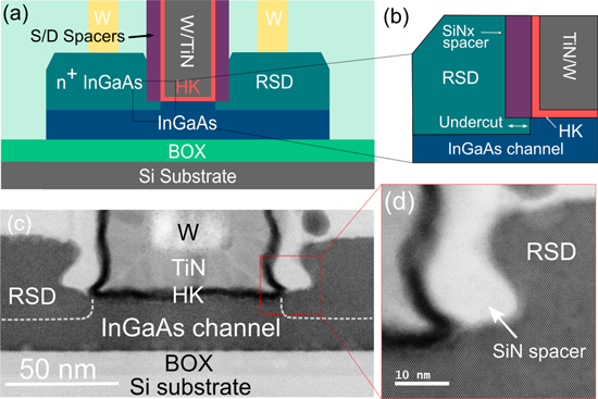
Fig. 1. (Color online) (a) Schematic cross-section of the fabricated InGaAs-on-insulator FinFET devices, including RSD epitaxy and SiN spacers. (b) Zoom-in schematic on the gate side, showing the undercut region formed by digital etching to create doped extensions. (c) STEM cross-section of a 60 nm gate length device. The dashed line indicates the interface between the channel and the RSD region. (d) STEM image on the gate side showing the 10 nm SiN spacers and the high crystalline quality of the III–V region.
Download figure:
Standard image High-resolution imageAfter forming the SiNx sidewall spacers, we use a digital etching (DE) process to selectively remove parts of the InGaAs channel, as schematized in Fig. 2(a) (inset).21,22) In order to maintain low access resistance, the target undercut thickness must be matched with the spacer thickness, to result in an accurate alignment of the junction position underneath the gate region. The DE is performed in two steps: 8 min oxidation in a UV–Ozone chamber and etching in HCl:H2O (1:10). By measuring the channel thickness with atomic force microscopy (AFM), we determine the etching rate of 1 nm/cycle as shown in Fig. 2(a). Similar etch rates were observed for InP DE in another work.23) The stable etch rate achieved with this method is due to the approximately saturated oxidation of the InGaAs surface, following Lukeš' rate law.24) The diluted HCl subsequently completely etches the formed native oxide but is selective to the semiconductor itself. AFM measurements performed on the larger contacts area [visible in Fig. 2(d)] show significant improvement of InGaAs RMS surface roughness from 0.9 to 0.3 nm [Fig. 2(a)]. SEM pictures of the gated fins before and after the RSD steps are displayed in Figs. 2(b)–2(d).
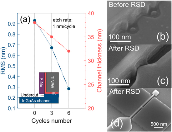
Fig. 2. (Color online) (a) RMS roughness values measured by AFM (left) improve by increasing the number of digital etching cycles. On the right, channel thickness measurement is used to monitor the etching rate per cycle (1 nm/cycle) (b) SEM image displaying gated fins after DE and before RSD. (c) SEM image of gated single-fin after RSD and (d) overview of the device after RSD.
Download figure:
Standard image High-resolution imageFigure 3(a) shows the transfer characteristic of an LG = 20 nm device with WFIN = 15 nm. This device shows ION = 350 μA μm−1 (IOFF = 100 nA μm−1 and VDD = 0.5 V), drain-induced barrier-lowering DIBL = 30 mV/V and inverse subthreshold slopes in the linear and saturation regions, SSLIN = 74 and SSSAT = 78 mV/decade, respectively. The reported ION is among the highest for Si CMOS-compatible III–V FETs. The gate leakage (not shown) is lower than 1 × 10⁻¹⁰ A μm−1. We achieve a peak transconductance value of about 1.5 mS μm−1. In comparison to our previous work,25) based on devices featuring no spacers, we lower the off-current by approximately 3 orders of magnitude, resulting in a subthreshold slope improvement near the off-current target and thus an overall increase in ION. Detailed analysis of the influence of the spacers on the off-state performance26) as well as noise characterization27) was reported elsewhere. Figure 3(b) displays the output characteristic for the same device, showing healthy transistor characteristics with low output conductance. The on-resistance for this device is 300 Ω μm. Excellent performance is also achieved in ultra-scaled devices. As, shown in Fig. 3(c), we report ION = 300 μA μm−1 (IOFF = 100 nA μm−1 and VDD = 0.5 V) for a device with LG = 13 nm and WFIN = 25 nm. As displayed in the benchmarking plot [Fig. 3(d)], this value represents the highest reported on-current for ultra-scaled CMOS-compatible III–V MOSFETs integrated on silicon.20,25,26,28–30)
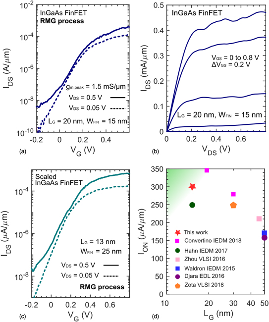
Fig. 3. (Color online) (a) Transfer and (b) output characteristic of InGaAs FinFET with LG = 20 nm and WFIN = 15 nm. The device exhibits an on-current of 350 μA μm−1 at fixed IOFF off 100 nA μm−1. (c) Transfer characteristic of the shortest gate length device (LG = 13 nm and WFIN = 25 nm) featuring an on-current of 300 μA μm−1 at fixed IOFF off 100 nA μm−1. This value is the highest reported for scaled III–V FinFETs on silicon. (d) Benchmarking plot showing ION (IOFF = 100 nA μm−1, VDD = 0.5 V) versus LG for different III–V-on-Si technologies. The green-shaded area highlights the preferred operation region.
Download figure:
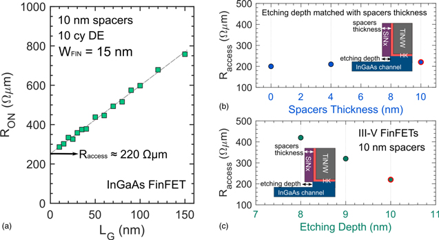
Standard image High-resolution imageIn Fig. 4(a), on-resistance versus gate length for InGaAs FinFETs with WFIN = 40 nm is shown. We extrapolate an access resistance of about 220 Ω μm. To assess the effectiveness of the implemented process modules we evaluate the access resistance for samples with different spacer thickness (0 nm, 4 nm and 10 nm) with S/D extensions matching the spacer thickness, as shown in Fig. 4(b). Raccess increases from 200 to 220 Ω μm, for devices without spacers to devices with 10 nm spacers, showing that a relatively low Raccess can be maintained by matching spacer thickness with SD extension length. Devices with different extension lengths (8, 9 and 10 nm) at fixed spacer thickness (10 nm) are also shown in Fig. 4(c). A mismatch of 2 nm between spacer thickness and SD extension length results in a 200 Ω μm increase in Raccess, (approximately 100 Ω μm per nm of mismatch) demonstrating a strong need for a highly controllable SD extension formation process.
Fig. 4. (Color online) (a) ON resistance versus gate length for InGaAs FinFETs with WFIN = 40 nm. An access resistance of about 220 Ω μm extrapolated. (c) Access resistance for 3 different spacers thickness where the undercut length is equal to the spacers thickness. The number of cycles determines the undercut length, as shown in the inset. (b) Access resistance for different number of cycles performed on the 10 nm spacers devices (corresponding to different etching depths). The red circle indicates the optimum point in terms of spacers thickness and number of etching cycles. The use of extensions regions clearly prevents the access resistance degradation but a careful matching of the undercut position w.r.t. the spacers is crucial to benefit from it.
Download figure:
Standard image High-resolution image
In summary, III–V on silicon MOSFETs are susceptible to large OFF-state leakage currents through the floating body effect and PBE. In this work we explored the use of spacers to reduce the PBE. We demonstrated high-performance InGaAs FinFETs integrated on silicon using carefully designed RSD extensions. At LG = 13 nm we achieve an on-current of 300 μA μm−1 (IOFF = 100 nA μm−1 and VDD = 0.5 V), among the highest reported values for ultra-scaled Si CMOS-compatible III–V FETs. We showed that Raccess increased by ∼100 Ω μm per nanometer of mismatch between the spacer thickness and SD extension length, as well as that relatively low Raccess can be maintained with effective matching between spacers and extensions. This highlights the need for a highly controllable SD extension formation process for high-performance III–V FETs.
Acknowledgments
The authors want to acknowledge the BRNC staff for technical support. This work was funded by Horizon 2020 grant agreement no. 688784 (INSIGHT) and grant agreement no. 687931 (REMINDER).