
Abstract
Thin-film transistors (TFTs) using metal oxide semiconductors are very promising as driving elements of next-generation displays, and their development is rapidly progressing. However, compared to conventional Si TFTs, they exhibit numerous problems with reliability. In this paper, we outline the observations of various degradation phenomena against electrical bias stress under DC and AC voltage, discuss the degradation mechanism, introduce gate insulation film and protective film which contribute to the improvement of reliability, and propose a reliability evaluation technique using an IR microscope.
Export citation and abstract BibTeX RIS
1. Introduction
Studies on thin-film transistors (TFTs) using metal oxide semiconductors1,2) have been carried out for a long time, but after the report by Ref. 3 in 2004, research on amorphous oxide TFTs rapidly increased. In addition, research by Ref. 4 in 2006 has further accelerated the research towards practical application. Today, the mass production of metal oxide semiconductors has begun as a driving transistor for LCD and organic EL. Furthermore, various research is being carried out with the goal of increasing its performance, improving reliability and reducing the cost.
Compared to amorphous Si5–7) and low-temperature polycrystalline Si,8–16) which have been put into practical use up to now, metal oxide TFTs suffer from specific deterioration phenomena, which have been reported by various researchers. In this paper, we outline our observations of various degradation phenomena against electrical bias stress under DC and AC voltage, discuss several mechanisms that induce the deterioration of oxide TFT reliability, introduce innovative methods to process gate insulation film and protective film to improve reliability, and propose a new evaluation technique using an IR microscope, with the purpose of further enhancing the reliability and performance of oxide TFTs.
2. Degradation phenomena of amorphous-oxide-semiconductor TFT by constant voltage bias stress
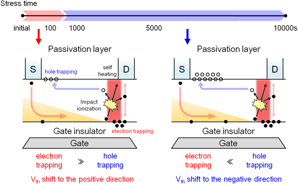
Degradation by electrical stress in metal oxide semiconductor has been one of the critical issues in the development of thin-film devices.17–38) Several previous studies on the reliability of TFTs using ZnO for the semiconductor layer have been reported,17,18) but for the first time we report the degradation by applying a positive bias voltage to the gate of amorphous InGaZnO (a-IGZO) TFT. We observed the degradation phenomena characterized by the positive parallel shift of the transfer characteristics after positive gate bias application and proposed the degradation mechanism.19) As shown in Fig. 1, when a positive voltage was applied to the bottom-gate-type a-IGZO TFT with a nitride film as the gate insulating film, a change in its transfer characteristic was observed. Figure 2 shows that the transfer curve was shifted parallel to the positive direction and the variation of threshold voltage was large. In addition, the amount of threshold value increased with the increase of the applied voltage. The level of degradation was observed to be in a linear relationship with the stress time duration. The gradient became more moderate when increasing the stress voltage. In addition, as shown in Fig. 3, changing the gate length and width, yields different deterioration rates in threshold voltage shift, but almost minimal change in the slope was observed. As for the absolute amount, the larger the gate width and length were, the larger the absolute amount of voltage shift was observed.

Fig. 1. Cross-sectional image of IGZO TFT.19)
Download figure:
Standard image High-resolution image
Fig. 2. (Color online) Degradation of transfer characteristics by gate voltage stress of 20 V. With the passage of time, the transfer curve shifted parallel to the positive direction.19)
Download figure:
Standard image High-resolution image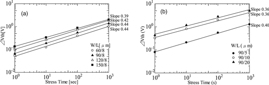
Fig. 3. Threshold voltage shift under gate voltage stress of 30 V measured at various gate widths (a). Gate length dependence measured for gate voltage stress of 30 V (b).19)
Download figure:
Standard image High-resolution imageNext, when the electric bias stress was applied and subsequently removed, recovery behavior was seen. As shown in Fig. 4, the deteriorated transfer characteristics induced by the positive bias stress (PBS) application for 10000 s are almost recovered after leaving the TFT without any bias for 10000 s. The recovery amount of the threshold was also linear with respect to time. Therefore, based on the experimental results, the degradation mechanism was considered as follows. Unlike Si-based TFTs, the change in threshold voltage seen in a-IGZO TFT is thought to be caused by the trapping of electrons at the interface due to gate bias stress. Since it is almost recovered by just leaving the TFT after stress application, the degradation is caused by traps existing at a very shallow energy level. In addition, it is considered that a new density of state (DOS) due to the bias stress could not be formed, since the slope of the transfer characteristic hardly changed with respect to stress application, as shown by the parallel shifting. Device simulation based on this model demonstrated the deterioration phenomena. In the device simulation, a clear threshold voltage shift was observed by increasing the shallow trap density.
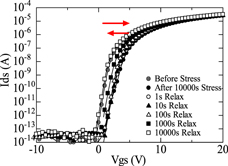
Fig. 4. (Color online) Recovery of electrical properties after stress imposition. After the imposition of gate voltage of 20 V, the recovery of electrical properties was measured without any stress at RT.19)
Download figure:
Standard image High-resolution image3. Improvement of reliability by fluorinated nitride film
For improving the reliability against bias stress, we proposed a fluorinated nitride film by introducing fluorine into the gate insulating film during deposition.39) From our initial experimental results of film deposition using various kinds of gases, we found that fluorine strongly correlates with superb reliability against the bias stress of oxide TFT. Inductively-coupled plasma-enhanced chemical vapor deposition (ICP-CVD) using SiF4 /N2 as the source gas was adopted. As a result, we fabricated a-IGZO TFTs with a high-quality fluorinitride film as a gate insulating film and succeeded in suppressing the shift in the threshold voltage. Changes in transfer characteristics against bias stress were measured using a TFT with a bottom-gate top-contact structure, as shown in Fig. 5. In order to confirm the effects of fluorine and hydrogen, the fabrication conditions, as shown in Table I, were prepared. As a reference, a conventional nitride film containing hydrogen was also prepared. This conventional film was deposited by plasma-enhanced chemical vapor deposition (PECVD) at 400 °C to control the hydrogen content. If this film is deposited at lower temperature, the large amount of hydrogen will cause unstable TFT operation.
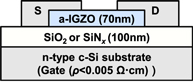
Fig. 5. (Color online) Device structure of a-IGZO TFTs.39)
Download figure:
Standard image High-resolution imageTable I. Fabrication conditions of each gate insulator.39)
| Sample | Gas ratio | Fabrication temperature |
|---|---|---|
| SiN:F | SiF4/N2 = 1/18 | 150 °C |
| SiN:F + F | SiF4/N2 = 1/6 | 150 °C |
| SiN:F + H | SiF4/N2 = 1/18 + H2 8% | 150 °C |
| SiN:H | SiH4/NH3 = 2/3 | 400 °C |
The distribution of hydrogen in the fluorinated silicon nitride film was investigated by secondary-ion mass spectrometry (SIMS) and it was found that 3.6 × 10²⁰ atom cm−3 of hydrogen, which was about 1/10 of the conventional SiN film, was uniformly distributed throughout the entire film. Figure 6 shows the results of the bias stress experiment of the TFT characteristics with the above four conditions. SiN:H, which is the conventional condition [Fig. 6(a)], has a threshold shift of about 2.5 V. For the fluorinated nitrogen, considerable improvement is observed against a bias stress of 10000 s with SiN:F [Fig. 6(b)] and SiN:F + H [Fig. 6(c)], having threshold shifts of 0.8 and 1.6 V, respectively. Compared to these three conditions, the shift amount also decreases as the hydrogen content further decreases. Furthermore, in the case of SiN:F + F [Fig. 6(d)], the shift amount was 0.1 V or less. In comparison, the threshold voltage shift of the a-IGZO TFT using SiO2 as the gate insulating film was 0.6–0.8 V, which further demonstrates the superior effectiveness of the fluorinated nitride film.
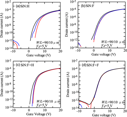
Fig. 6. (Color online) Transfer curves after PBS for a-IGZO TFTs utilized (a) SiN:H (b) SiN:F (c) SiN:F + H and SiN:F + F.39)
Download figure:
Standard image High-resolution imageThe mechanism was discussed as follows. In the fluorinated insulating film, the hydrogen content is smaller compared with the usual nitride film. The introduction of fluorine promotes reduction of the interface state density. From the analysis of X-ray photoelectron spectroscopy (XPS) at both the a-IGZO surface and its interface with the fluorinated SiN film, fluorine bonding with the metal was observed, which terminated the oxygen vacancies in the oxide-semiconductor film. Reference 40 further investigated this mechanism for improved reliability after fluorine incorporation in the gate insulating film. The results and analysis indicate that the incorporated fluorine exists at the interface in the form of In-Fx and In-OF, as shown in Fig. 7, leading to the reduction of the interface state. The reduction of the bonding states at the IGZO and gate insulator interface resulted in the decrease of the number of tail states near the conduction band minimum.

Fig. 7. (Color online) In 3d peaks in the a-IGZO bulk (blue line) and at the a-IGZO/SiNx:F interface (red line) obtained by XPS measurements.40)
Download figure:
Standard image High-resolution image4. Degradation by negative bias illumination stress (NBIS)
The phenomenon where the threshold voltage is greatly shifted to the negative direction when light irradiation is applied while applying negative bias is a typical degradation phenomenon observed in oxide TFT. Many reports have also been published on this issue.41–66) Reference 41 investigated the effect of irradiating gallium-indium-zinc-oxide (GIZO) TFT with light, while applying negative voltage. This stress combination greatly accelerated the threshold voltage shift in the negative direction. This is directly attributed to the fact that carriers induced by light are trapped at the interface between the gate insulating film and semiconductor, and this phenomenon is reported to be accelerated depending on the environmental conditions, such as moisture. Reference 42 observed photodegradation phenomena by irradiating a-IGZO TFT with light at various wavelengths and electric power. It is confirmed that the shift of the threshold voltage depends on an increase in electric power, irradiation time and a decrease in wavelength. Reference 43 proposed that oxygen vacancies acting as hole traps are the main cause of light-bias degradation. They proposed a model in which optically excited holes move to the channel/insulating film interface and are captured in oxygen vacancies (Vo) in the dielectric layer. Since IGZO is amorphous, Vo2+ defects are less likely to revert to their original defect state. Moreover, even if electrons are trapped, the shallow defect level is maintained. In addition, this shows that additional heat treatment removes hole traps and is effective for recovering the device reliability.
Reference 46 observed that the threshold voltage shifts by just irradiating light at 365 nm on the oxide-semiconductor channel. The deterioration depends on the thickness of the active layer, and the TFT with a thickness of 20–50 nm exhibits a large change, which was further aggravated by the bias. It is considered that this phenomenon is caused by a metastable state induced by light and that the state is related to ionized oxygen vacancies. Reference 47 compared negative bias illumination degradation using an a-IGZO TFT having SiO2 and SiNx as a gate insulating film. As a result, a very large threshold shift is observed in the SiNx TFT. The reason is that the trapping level, which exists abundantly at the SiNx interface, captures the photoexcited holes. Through this method, the trapping is greatly recovered even at RT and almost wholly recovered after heat treatment at 250 °C, so the trap is considered to be temporary.
Reference 48 estimated the sub-gap state generated by photodegradation from the evaluation of the light-bias deterioration phenomenon by examining the capacitance–voltage (C–V) characteristics. The level is due to ionized oxygen vacancies. Furthermore, it is considered that photo-excitation from Vo to stable Vo2+ supplies free electrons to the conductor and the increased electron further accelerates the negative voltage shift. Reference 50 observed a large negative voltage shift by irradiating a TFT having Hf-In-Zn-O (HIZO) as an active layer with UV light. This is because UV light contributes to the generation of defects, which are trapping sites for the photoinduced holes and the generated oxygen vacancies capture holes induced by UV light, thereby forming dual oxygen vacancies (Vo2+).
Reference 52 analyzed the dependence of the light-bias degradation with the film thickness (20, 50 and 100 nm) of the active layer. The results of the current–voltage characteristic (I–V) and the capacitance–voltage (C–V) point to the formation of double donors (Vo2+) in the bulk associated with oxygen vacancies. Moreover, from the C–V characteristics, it is confirmed that the gap level (Ec – E) is broadly distributed from 0.3–1.0 eV. Reference 53 investigated the temperature dependence of the photodegradation phenomenon and estimated that the deterioration accelerated as the temperature increased and its activation energy was 1.06 eV. In addition, they can describe the change of threshold with a stretch exponential function and their study suggests that oxygen deficiency is involved in its mechanism. Reference 54 reported that light-bias degradation is generated by light irradiation under the application of a negative voltage and its origin is a hole trap such as oxygen vacancies. They analyzed the effect of hydrogenation on NBIS degradation using first principles calculations. They insist that oxygen vacancies causing NBIS are passivated by hydrogen because oxygen vacancies (Vo) replaced by hydrogen (Ho) are more stable than when bonded in the gap. The desorption of hydrogen from Ho and the diffusion energy of hydrogen at the interface (Hi) are calculated to be 1.27 and 0.51 eV, respectively. Also, since Ho defects are stable after heat treatment up to 200 °C, it is concluded that hydrogenation not only reduces oxygen vacancies, but has the effect of suppressing NBIS. Reference 55 found that recovery phenomena against light-bias degradation is accelerated by PBS, based on I–V characteristics and C–V characteristics of TFTs. When the trapped positive charge is released, the ionized oxygen vacancy is neutralized by electron capture and recovers to its original deep level.
Reference 66 discussed the degradation under NBIS in a-InGaZnO TFT. They made a-IGZO TFT on a glass substrate, applied a combination of negative bias stress (NBS) and light irradiation (NBIS) and evaluated the change of DOS of the TFT. For an NBIS of −20 V, the threshold voltage shifted towards the negative direction, but an increase of shallow states expected as positively ionized oxygen vacancies (Vo+ or Vo++) were not observed in the DOS curve. On the other hand, for NBIS of −30 V, change in the DOS near the conduction band edge before and after applying a bias stress was observed. This suggests that Vo+ or Vo++ was generated by NBIS, but the accumulation of holes at the a-IGZO/SiO2 interface mainly caused the threshold voltage shifts, as shown in Fig. 8.

Fig. 8. (Color online) Illustration of the instability mechanism for (a) NBS of −20 V, (b) NBIS of −20 V and (c) NBIS of −30 V. Note that the unknown defects were passivated easily by photoexcited electrons, and Vo+ and Vo++ are unstable under EF. Blue arrows indicate possible movement of electrons.66)
Download figure:
Standard image High-resolution image5. Reliability improvement by protective film with siloxane
Numerous studies have been undertaken where attempts have been made to reduce the deterioration of the characteristics of oxide-semiconductor TFTs through a protective film.67–89) Reference 67 investigated the influence of atmospheric air on a-IGZO TFT. In ambient air, the threshold value was −7 V. As the degree of vacuum increased from the outside air, the threshold voltage shifted to negative voltage, while the threshold voltage shifted to the positive direction as the oxygen pressure was increased. The reason for this is that adsorption of oxygen to the back interface forms a depletion region and the carrier concentration varied in the range of 1 × 10¹⁹ to 1 × 1020 cm−3. Reference 68 fabricated ZnO TFTs at atmospheric pressure using an atomic layer deposition (ALD) process with a process temperature below 200 °C. They reported superior characteristics against PBS by depositing 100 nm of Al2O3 as passivation.
Reference 69 investigated the effect of moisture on the a-IGZO TFT. Water diffused into the a-IGZO thin film, thereby reversibly changing the transistor characteristics. Depending on film thickness, two competitive mechanisms are clarified. For films thicker than 100 nm, additional electrons were introduced due to the absorption of moisture, while acceptor-type behavior induced by moisture is observed in thin films of 70 nm or less. This direct proof is indicated by the marked deterioration of the S value in the 30 nm thin a-IGZO thin film. Reference 70 irradiated the backside of a-IGZO with N2O plasma to prevent the removal of In-rich regions and entry of hydrogen. As a result, they obtained high mobility of 37 cm2 V−1 s−1 and S value of 0.25 V decade−1.
Reference 71 examined the effectiveness of passivation layers by using organic photo acryl (PA) and a-IGZO TFT with PECVD-SiO2 passivation. Compared with PA, TFT with SiO2 passivation showed excellent control of the threshold shift and S value change against PBS. As a mechanism for causing a positive threshold voltage shift when a positive bias is applied, adsorption of oxygen molecules from the atmosphere captures electrons in a-IGZO and positively charged water molecules on the surface desorbs. Therefore, this showed that threshold shift can be suppressed by sufficient passivation of the IGZO back channel. Reference 72 investigated the effect of adding water to the annealing atmosphere of a-IGZO TFT. Dry O2 annealing improved the mobility and S value, but wet O2 annealing further improved mobility to 12 cm2 V−1 and S value to 0.12 V decade−1. The elimination of hydroxyl groups promoted the improvement of conductivity. Zn–O bonds began to desorb from the dry O2 annealing at about 300 °C, but in the wet O2 annealing they were considerably suppressed.
Reference 73 investigated the change in threshold voltage of a-IGZO TFT under constant current stress. The TFT was fabricated at RT and was either annealed in a dry O2 atmosphere at 400 °C or a wet O2 atmosphere. All the thresholds indicated a positive shift and the shift amount was suppressed by annealing. By performing TFT simulation, threshold variation is explained by deep-level defects and large shifts in TFTs without annealing are explained by increased shallow levels. Reference 74 evaluated the threshold shift for gate bias stress in vacuum, hydrogen, oxygen and air atmosphere. As a result, the change in the hydrogen atmosphere was more conspicuous compared with oxygen. The reason for this is that an accumulation layer is formed on the a-IGZO surface after exposure to hydrogen.
Reference 75 evaluated the reliability of a-IGZO TFT with paraffin wax as passivation. This film can be formed by the sol–gel method under atmospheric pressure and it has high yield at low cost. This TFT exhibits a low threshold fluctuation with respect to moisture, oxygen, air and the like. In addition, changes in characteristics were small with respect to light irradiation. From the analysis, it is established that this is influenced by the low DOS. Reference 76 performed experiments to passivate electron traps in a-IGZO film with hydrogen. Annealing at 300 °C showed good operating characteristics, but it deteriorated at 400 °C or more. Thermal desorption spectra of water shows that the critical point of temperature is related to water desorption. The re-doping of hydrogen by wet oxygen annealing shows a recovery to achieve excellent TFT characteristics. The binding energy of hydrogen that passivates the trap corresponds to desorption at 300 °C–430 °C. The model was proposed from these results.
References 77–79 demonstrated that a-IGZO TFT with passivation based on polysilsesquioxane (PSQ) has strong reliability against PBS, NBS and light-illumination bias stress. They explain that hydrogen from the PSQ film reduced oxygen vacancies and carbon forms acceptors in IGZO. Photosensitive polysilsesquioxane (P-PSQ) was also developed as a passivation film and was deposited by solution process via spin coating. For P-PSQ, no dry etching is required to form contact holes which circumvent the adverse effect associated with dry etching. Figure 9 shows the transfer characteristic shift of the TFT with P-PSQ as the passivation film due to the PBS and NBS. For comparison, a bias stress test was also carried out using a TFT having no P-PSQ passivation film. The TFT with P-PSQ shows considerably good stability. After 10000 s, the threshold shift was as small as 0.5 V. In contrast, TFTs with no passivation film shifted significantly by 5 V against PBS. Furthermore, small degradation in the subthreshold region was observed after 10000 s, which suggests additional defects and trap levels. Also, for NBS, the amount of change in TFT without passivation film is small, but a clear hump phenomenon was observed. Furthermore, a humidity test was carried out. Although the transfer characteristics of TFTs with P-PSQ hardly changed, in the absence of a passivation film, a shift of the threshold voltage value to the negative direction was observed. As a result of SIMS analysis, high H and F were confirmed in a-IGZO in TFT having P-PSQ, as shown in Fig. 10. They considered that this high concentration of hydrogen and fluorine reduces Vo.
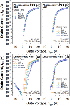
Fig. 9. (Color online) Evolution of transfer characteristics of photosensitive PSQ a-IGZO TFT (top row) under (a) PBS and (b) NBS. Evolution of transfer characteristics for unpassivated a-IGZO TFT (bottom row) after (c) PBS and (d) NBS. Stress condition: PBS (Vgs = 20 V); NBS (Vgs = −20 V).77)
Download figure:
Standard image High-resolution image
Fig. 10. (Color online) SIMS profile in the a-IGZO layer of (a) photosensitive PSQ (solid lines) and (b) unpassivated film samples (dashed lines). Green, red and blue lines represent 1.2 H, 19 F and/or 18 O + 1 H, and 13 C, respectively. The 0 nm depth is the side nearest the passivation layer. Note that fluorine is part of the photosensitive PSQ solution, while unpassivated TFT is not fluorinated.77)
Download figure:
Standard image High-resolution imageReference 80 demonstrated that Al2O3 films deposited by the ALD method are effective passivation films for a-IGZO TFTs. By using dimethylaluminum hydride (DMAH), which has only two methyl groups as ALD material, there are fewer impurities such as carbon and film with a high deposition rate can be formed, as shown in Fig. 11. For the positive gate bias of 20 V for 10000 s, considerably smaller threshold voltage shift was observed for TFT with DMAH compared with trimethylaluminum hydride (TMA). The reasons for showing high reliability against PBS compared with TMA, which is a conventional material, are as follows. Due to the XPS analysis, the bonding ratio of M-Vo is decreasing, which is likely due to hydrogen from DMAH passivating Vo in the a-IGZO film.

Fig. 11. (Color online) Transfer characteristics (Vds = 0.1, 5.0 and 9.9 V) of a-IGZO TFTs passivated with plasma-enhanced-ALD Al2O3 using (a) TMA or (b) DMA and annealed in O2 at 300 °C. The a-IGZO channel has a geometry of W/L = 90/10 μm. Inset shows the chemical structure of TMA and DMAH, where gray, red and white represent Al, C and H atoms, respectively.80)
Download figure:
Standard image High-resolution image6. Degradation phenomenon due to AC stress
In TFTs used for driving displays, a pulse voltage is applied to an electrode for both LCDs or OLEDs. Therefore, it is very important to confirm the change in performance when AC voltage is applied. Reference 90 evaluated the deterioration phenomena against AC stress by applying pulse stress using a-IGZO TFT. They observed degradation phenomena for S values that are not typically observed under DC bias stress. As for deterioration, it is considered that electrons with high energy form a level at the interface during the rising edge of the gate pulse. Figure 12 shows the change in the transfer characteristics when ±20 V is applied to the gate electrode of the a-IGZO TFT using SiN gate insulator film and 0 V is applied to the source and drain electrodes (Vd = 0 V). As time passes, the threshold changes in the negative direction and deterioration of the S value can also be observed. Figure 13 shows the change in S value for various pulse conditions. With the DC voltage of Vg = 20 V and Vg = −20 V, the S value hardly changes, but only increases with the application of pulse with time. Also, the level of change increases with increasing frequency. In order to investigate the cause of deterioration, the degradation amount was observed by changing the rise and fall time, as shown in Fig. 14. From these comparisons, it was obviously dependent on the fall time and it was found that the sharper the pulse the greater the TFT deteriorates. Therefore, they explain the deterioration mechanism as follows. When a positive bias is applied to the gate, electrons are induced at the interface and subsequently trapped at the interface. The captured electrons are released when they are negatively biased. Device simulation showed that a high electric field is generated at the source and drain when a negative bias is applied. Therefore, they considered that the emitted electrons are accelerated by this high electric field and further create interface states. In the case of rise time, electrons gather to the channel by PBS. However, the electric field is not so high and electrons are not accelerated to create the interface. So they concluded that degradation was clearly observed at falling time.
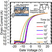
Fig. 12. (Color online) TFT properties under AC (±20 V, 500 kHz) stress. Transfer curves before and after 1, 10, 100, 1000 and 10000 s stress are shown. Inset shows the TFT structure investigated in this study.90)
Download figure:
Standard image High-resolution image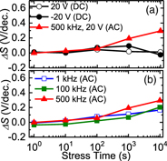
Fig. 13. (Color online) Changes of the S value caused by the AC and DC stress voltages. (a) ∆S with various stress voltage conditions. (b) ∆S with various stress frequencies.90)
Download figure:
Standard image High-resolution image
Fig. 14. (Color online) Transfer curves under AC stress with various gradients of transition edges. Results under the AC pulse stress including (a) the sharp rising edge and the slow falling edge, (b) the slow rising edge and sharp falling edge.90)
Download figure:
Standard image High-resolution image7. Thermal degradation and its analysis using an IR microscope
Heat generation phenomena have been proposed as a cause of TFT deterioration.91–95) Reference 91 observed the heat generation phenomena using amorphous InSnZnO (a-ITZO). For thermal analysis, an IR microscope (Infra Scope) using InSb as a detector was used. They investigated in detail the non-uniformity of heat generation in the gate direction and the size dependence. Figure 15 shows the state of heat generation when the Vd and the Vg are varied. The higher the gate voltage and drain voltage, the higher the heat generation temperature. When Vg = Vd = 30 V, the maximum temperature of 150 °C is observed. Although the 2D distribution is shown in Fig. 15, it can be observed that the peak of heat generation is asymmetric and leaned towards the drain side. When Vd > Vg, it was biased towards the drain side and symmetrical when Vd < Vg.
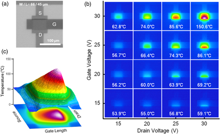
Fig. 15. (Color online) (a) Optical microscopic image of a TFT with a gate width of 66 μm and gate length of 45 μm used for thermal analysis. (b) Thermal distribution under various gate and drain voltages. (c) 2D image of thermal distribution with stress voltage of Vg = Vd = 30 V.91)
Download figure:
Standard image High-resolution imageNext, changes are observed in transfer characteristics when Vg = Vd = 20 V are applied to the ITZO TFT. As shown in Fig. 16, within the first 100 s, the transfer characteristics shift positively and then shift in the negative direction. The heat generation temperature also decreased in the first 10 s and then increased gradually. They discussed the mechanism, as shown in Fig. 17. Due to the high Vd, impact ionization occurs and electrons move to the interface between the semiconductor and insulating film. In addition, holes diffuse to the back channel and are trapped. Initially, the trapping of electrons is the main factor that causes positive threshold shift and decrease in heat generation. Then, hole trapping at the back channel becomes dominant, resulting in a negative threshold shift and an increase in heat generation. Nevertheless, the capture of holes at the back channel region, especially near the source and drain edge, also causes hump formation. The hole capture induces the creation of a parasitic transistor that turns on faster than the main transistor, thus creating the hump that is especially prevalent for TFTs operating in enhancement mode (normally OFF TFTs). Thus, this is the first report of the hot carrier phenomenon in metal oxide semiconductors.

Fig. 16. (Color online) Change of transfer curves of ITZO TFT with bias stress of Vg = 20 V and Vd = 20 V.91)
Download figure:
Standard image High-resolution image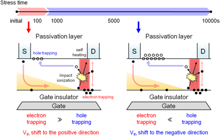
Fig. 17. (Color online) Degradation model with bias stress of Vg = Vd = 20 V in the early period (left) and in the second stage (right).91)
Download figure:
Standard image High-resolution imageFurthermore, Ref. 92 expanded on the discussion of the influence of heat generation using TFT with various lengths and widths. As a result, the heating effect strongly depended on the channel scale and severe threshold voltage shift and high heating temperature were observed for wider TFT. They concluded that reliability was affected by the accumulation of heat in wider TFT.
8. Heat deterioration phenomenon due to AC stress
Reference 96 investigated the deterioration phenomenon due to heat in a-IGZO TFT by using an IR microscope. By using the pseudo-interval measurement method, changes in heat generation phenomena for various operating frequencies are observed and the deterioration mechanism accompanying heat is discussed. By introducing the pseudo-interval measurement method, they succeeded in improving the measurement frequency (13.2 Hz) of the original device and it was above the measurement limit of the thermal analysis system. The principle is shown in Fig. 18. By shifting the frequency of the pulse applied to the element and the frequency of the CCD camera, it is understood that heat generation can be observed in sampled form. Figure 19 shows the relationship between frequency and temperature. At a low frequency of 10 Hz or less, the maximum and minimum temperature of the device show the values at the time of application of the respective DC voltage, but when the frequency is further raised, it becomes impossible to follow the temperature change. At 1 kHz or more, the highest and lowest temperature are in agreement. Its value became the median value at low frequency. Therefore, how the heat generation affects the characteristics of the device was investigated, as shown in Fig. 20.
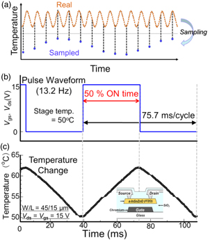
Fig. 18. (Color online) (a) Image of pseudo-measuring interval method; (b) applied pulse waveform; (c) pseudo-interval measurement results. Inset is the cross-sectional view of ITZO TFT.91)
Download figure:
Standard image High-resolution image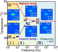
Fig. 19. (Color online) Frequency dependence of heat generation temperature.96)
Download figure:
Standard image High-resolution image
Fig. 20. (Color online) Vth shift under pulse stress at 10 Hz and 1 kHz stress test; (a) and (b) Ids–Vgs curve ((c) and (d) are enlarged images); (e) Vth shift.96)
Download figure:
Standard image High-resolution image
When pulses of 10 Hz and 1 kHz which changed the heat generation temperature were applied, the threshold voltage shifted in the positive direction at both frequencies, but the shift amount was larger at 10 Hz. Thus, this difference is thought to be caused by heat generation inside the TFT. The mechanism is discussed as follows. When a voltage is applied to the gate and the drain, electrons are accelerated by the electric field and they are captured at the interface between the semiconductor and insulating film, causing a threshold voltage shift. However, as the heating temperature is higher, the electron trapping is accelerated. At low frequency (10 Hz), the temperature at ON is higher than at high frequency (1 kHz). Therefore, considering the heat generation during operation is important for improving the reliability of the device, this analysis is crucial for the realization of flexible displays.
9. Summary
We reviewed the countermeasures for improving the reliability against electrical stress relating to TFTs using oxide semiconductors, focusing on the research content that we have been working on so far. First, we outlined the degradation phenomena and mechanism in IGZO TFT when a positive voltage was applied to the gate. It is concluded that the deterioration is mainly caused by electron injection into the shallow interface state, because the transfer characteristic is shifted in parallel and because the recovery phenomenon is observed when we stopped the stress. As a countermeasure for the degradation, a gate insulating film containing fluorine was proposed. From XPS analysis, we concluded that fluorine has an oxygen deficiency suppressing effect. Then, we examined the degradation mechanism due to the application of simultaneous light and NBS, which induces a large negative shift of the threshold value by analyzing the interface state through C–V measurement. In addition, in order to suppress deterioration against electrical bias, the introduction of a protective film using siloxane was proposed. We proposed that the key reaction is the reduction of oxygen defects by hydrogen from the protective film. Furthermore, we proposed the deterioration mechanism when AC stress is applied as electrical stress and a new degradation phenomenon when heat generation occurs. Thermal analysis using IR has proved that not only the temperature distribution of the device can be accurately determined, but the precise change in temperature while in actual operation.
The reliability improvement methods and evaluation techniques introduced in this paper will greatly contribute to the future development of next-generation flexible devices using oxide semiconductors.
Acknowledgments
The authors thank Prof. M. Furuta from Kochi University of Technology, Prof. M. Kimura from Ryukoku University and Prof. T. Kamiya for their helpful discussions. The authors also thank Dr. Y. Ando and Dr. D. Matsuo from Nissin Electric, Dr. T. Nonaka and Dr. N. Yoshida from Merck, Dr. S. Maeda and Dr. T. Isaji from the Nissan Chemical Corporation and Dr. K. Takahashi from Nippon Aluminum Alkyls, for their kind technical support.
Biographies

Yukiharu Uraoka was born in Tokushima, Japan, in 1961. He received the B.S., M.S. and Ph.D. degrees in Electrical and Electronics Engineering from Toyohashi University of Technology, Aichi, Japan, in 1983, 1985 and 1994, respectively.In 1985, he joined Panasonic Company Ltd., Osaka, Japan, where he has been engaged in the research of the reliability of CMOS devices and low-temperature poly-Si display devices. Since 1999, he has been a Professor of the Graduate School of Material Science, Nara Institute of Science and Technology (NAIST), Nara, Japan. His current research interest involves the fabrication of thin-film devices using Si film and oxide film and GaN power devices.

Juan Paolo S. Bermundo was born in the Philippines in 1987. He received his Ph.D. degree in Materials Science from Nara Institute of Science and Technology (NAIST) in 2015. Previously, he was an Instructor in the Department of Physics at Ateneo de Manila University, where he also received his M.S. degree in Physics in 2012 and his B.S. degrees in Physics and Materials Science and Engineering. In 2015, he joined NAIST as a specially appointed Assistant Professor. His research interests include oxide semiconductors, solution-processed materials and the low-temperature processing of flexible semiconductor devices.

Mami N. Fujii was born in Japan, in 1983. She received the B.E. degree in Electrical Engineering from the National Institution for Academic Degrees, Japan. She was a member of Professor Yukiharu Uraoka's group at the Nara Institute of Science and Technology in 2007 and started to work on electronic devices using oxide semiconductor. She later achieved her Masters degree in Engineering in 2009. She is currently a Research Fellow of the Japan Society for the Promotion of Science (JSPS) and received Ph.D. degrees in Engineering from the Nara Institute of Science and Technology, Japan, in 2012. Her interests include oxide-semiconductor reliability, interface analysis, device process and the development of high-performance TFT. She won the Young Researcher Award from the International Conference on Solid State Devices and Materials (SSDM) in 2011 and the Promotion and Nurturing of Female Researchers Contribution Award from the Japan Society of Applied Physics. Her research interests include the reliability of oxide semiconductor and diamond devices.

Mutsunori Uenuma was born in Nagano, Japan. He received Ph.D. degrees from Kyushu University in 2009. He has been a Research Assistant Professor at the Nara Institute of Science and Technology (NAIST) and Osaka University. Since 2014, he has been an Assistant Professor at NAIST. His current research interest involves thermoelectric devices and GaN power devices.

He received Ph.D. degrees in Electronics Engineering from the Nara Institute of Science and Technology, Japan, in 2003. After graduation, he undertook a post-doctoral fellowship at the Institut für Physikalische Elektronik, Universität Stuttgart, Germany, researching wearable photovoltaics. From 2005, he was a post-doctoral fellow at the Department of Physics and Astronomy, University of Toledo, USA, researching multi-junction amorphous silicon-based solar cells. In 2006, he joined Sharp corporation, Japan, where he had been engaged in the research of solar cells. Since 2010, he has been an Associate Professor of the Graduate School of Materials Science, Nara Institute of Science and Technology, Japan. His current research interests involve the application of nanostructure for energy harvesting, the processing of printed electronics, oxide materials and devices, and the reliability of photovoltaics.