

Abstract
We present a theoretical study on the gain and threshold current density of III-nitride quantum dot (QD) and quantum well (QW) lasers with a comprehensive theory model. It is found that at transparency condition the injection current density of QD lasers is about 120 times lower than QW lasers in III-nitrides, while in III-arsenide it is about 15 times. It means that using QDs in III-nitride lasers could be 8 times more efficient than in III-arsenide. This significant improvement in III-nitrides is due to their large effective-masses and the large asymmetry of effective-masses between valence bands and conduction bands. Our results reveal the advantages of using QD for low threshold laser applications in III-nitrides.
Export citation and abstract BibTeX RIS

Content from this work may be used under the terms of the Creative Commons Attribution 4.0 license. Any further distribution of this work must maintain attribution to the author(s) and the title of the work, journal citation and DOI.
1. Introduction
III-nitride semiconductor lasers have a broad range of applications,1–7) such as optical communications, high-brightness white lighting and material processing.8–14) However, the threshold current densities (Jth) of III-nitrides lasers are usually quite high. For example, InGaN quantum well (QW) lasers have typical Jth values of 1–4 kA cm−2, or even higher.15–19) Indeed, the imperfections in crystal growth and electrode fabrication could play important roles in the large Jth values, whereas other factors in III-nitrides should also be taken into accounts, i.e., the large effective-masses of carriers (  in conduction bands and
  in valence bands) and their large asymmetry (
 ).
).
As known, under parabolic approximation assumptions for band structures, the density of states (ρ(E)) in three dimensional (3D) bulks ( ) and two dimensional (2D) QWs (
 ) increase with effective-masses of carriers. Large densities of states result in a slow increasing of quasi Fermi levels, and thus higher threshold of injected carriers for lasing. Most importantly, in semiconductors that have a large asymmetry of effective-masses (
 ), normally the quasi Fermi level of holes (
 ) is above the top of valence band, so the quasi Fermi level of electrons (
 ) has to rise above the bottom of conduction band to satisfy Bernard-Duraffourg condition (
 ).20) Consequently, semiconductors with a large
  value would need a higher injection carrier density Ntr to reach transparency condition (with the gain g = 0) and would Require a higher injection threshold to reach lasing conditions than the ones with symmetric effective-masses (
 ).21)
).21)
There are mainly two ways to overcome the effective-mass asymmetry in order to realize lasers with low threshold currents. One is to relax the effective-mass asymmetry, usually by decreasing  in valence bands via strain-induced band-mixing effects.20) The other way is to change the dimensionality of active layers, such as using 2D QWs or 1D quantum wires.22) Nevertheless, even in the 1D and 2D structures with strain engineering, the
  effects still exist, through the effective-mass-related density of states. Whereas, zero dimensional quantum dots (QDs) are expected to terminate the effect of
  with a δ-function-like density of states that has no direct relation with effective-masses, and thus lasers made with QDs can exhibit extremely low lasing thresholds.22) Therefore, given the large effective-masses and their large asymmetry of
  in III-nitrides, applying QDs to low threshold lasing applications should be more important and more advantageous than in other material systems, such as in III-arsenide, which has relatively smaller effective-masses and smaller asymmetry of
  (much closer to 1).21)
In this work, we perform detailed theoretical calculations on the modal gain and threshold current densities of ridge-type InGaN QD and QW lasers with a comprehensive theory model, which includes the strain and polarization fields in active layers, k·p method for band structures, the non-uniform optical-mode distribution in laser structures and inhomogeneities of carrier distributions. We find that at transparency conditions, the required current density for lasing in QD lasers is 118 times smaller than in QW lasers. In addition, the threshold current densities of InGaAs lasers are also calculated and the improvement of InGaAs QD lasers over InGaAs QW lasers is only 15 times at transparency condition. The different improvement of using QDs over QWs between InGaN and InGaAs lasers is expected to be due to the different effective-masses and different  values. These results show that III-nitride QDs could be more advantageous than III-arsenide QDs for low threshold laser applications.
2. Calculation models
The InxGa1−xN QDs are formed on a 0.5 nm thick wetting layer with a density  and are surrounded by InyGa1−yN barriers. The indium composition x and y are set to be 0.2 and 0.02, respectively.23) The QDs have truncated hexagonal pyramid shape, with top width a = 3 nm, basal width b = 6 nm and height h = 2 nm [see Fig. 1(a)]. In order to compare the InGaN QD lasers with InGaN QW lasers, InxGa1−xN/InyGa1−yN QWs with a well thickness LQW = 1.6 nm are employed. Here the specific LQW value is chosen to have the same ground-state transition energy as QDs.

Fig. 1. (Color online) Schematic illustrations of (a) InGaN QDs used in calculations, (b) ridge-type laser structures for InGaN QDs and InGaN QWs, (c) the non-uniform distribution of optical modes for active layers at different positions. (d) The optical confinement factors of active layers located at different position in the waveguiding layer.
Download figure:
Standard image High-resolution imageLaser structures are assumed to be grown on c-plane GaN templates, with a 300 nm thick waveguiding layer sandwiched between two AlGaN cladding layers. The lower cladding layer is 600 nm thick and the upper one is 500 nm thick. Then a 200 nm thick GaN layer is capped at the top and a 2 μm-wide ridge is formed by etching down to the bottom of the top cladding layer [see Fig. 1(b)]. In the waveguiding layer [Fig. 1(c)], there are 20 periods of active layers (QD or QW layers, the period length is set as 7 nm), followed by a 20 nm thick AlGaN stop layer. The optical-mode distribution  of transverse electrical field
  over the laser cross-section is obtained by solving Maxwell's equations, as shown in Fig. 1(b). The optical confinement factor of the ith active layer is calculated by
for QD lasers, and
for QW lasers, where VQD and  are the QD's volume and height, respectively. Note that y-axis is along the ridge direction and z-axis is along sample's growth direction.
Figure 1(d) presents the calculated optical confinement factor (Γ) of each active layer, from which we see that the optical confinement factors show a strong non-uniformity for active layers at different positions: the most-outside layers have Γ values of only about a half of the central layer. Thus, in order to have a meaningful analysis of lasers with multi active layers, the non-uniformity of optical confinement factors in the waveguiding layer has to be taken into accounts.
3. Calculation methods
The strain distribution of QDs is obtained by minimizing the elastic strain energy.24) For the band structures and wavefunctions of both QDs and QWs, an effective-mass Hamiltonian based on single band envelope approximation is applied for electrons and a  Hamiltonian matrix derived from k·p theory is applied for holes.25,26) The material gains of a single QD-layer and QW-layer are calculated respectively by25,27,28)
and
where  index η denotes spin-up and spin-down states of electrons in conduction bands, index m denotes sub-bands in conduction bands, index n denotes sub-bands in valence bands,
  is the energy level of the mth sub-band in conduction bands,
  is the energy level of the nth sub-band in valence bands,
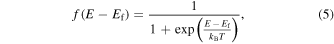
  is the momentum matrix element, f is the Fermi–Dirac distribution function defined as
the lineshape function Lγ is defined as

to account for the homogeneous broadening, and
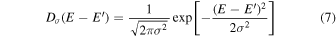
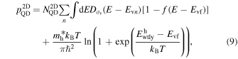
to account for the inhomogeneous broadening. The inhomogeneous broadening is also included in the calculation of quasi Fermi levels Ecf in conduction bands and Evf in valence bands, by using the carrier density relations
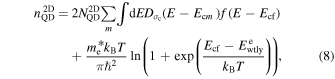
for QD lasers, and
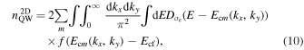
for QW lasers, where  (
( ) is the effective-mass of electrons (holes),
  (
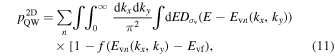
( ) is the ground-state energy of electrons (holes) in the 0.5 nm thick wetting layer and n2D (p2D) is the surface density of electrons (holes) per active layer. The factor "2" in Eqs. (8) and (10) accounts for two different spin states in conduction bands, since the single band envelope approximation is applied to electrons. The factor "2" disappears in Eqs. (9) and (11) because two spin states have already been considered in the 6 × 6 Hamiltonian for valence bands. The radiative current density is calculated with

where Leff is the effective thickness of active layers (Leff = LQW for QW layers and  for QD layers) and
  is the spontaneous emission rate per unit volume per unit energy interval (s−1 cm−3 eV−1),25) with
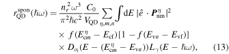
for QD lasers, and
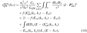
for QW lasers.
In calculations, we use the material parameters recommended by Ref. 29 and we set T = 300 K. The homogeneous broadening parameter γ is set as 5 meV, corresponding to a dephasing time of about 0.1 ps.30) For the inhomogeneous broadening parameters, we assume σc = 10 meV, σv = 2.5 meV, and thus  = 10.31 meV, which corresponds to a full-width-at-half-maximum value of 24.2 meV (
 ), just in between the values used in Refs. 28 and 31. The same broadening parameters are used in both QD lasers and QW lasers for simplicity.
4. Results and discussion
Figures 2(a) and 2(b), respectively, show the modal gain spectra (Γg) of QD and QW lasers with a single active layer under varying injection levels, where the single active layer is assumed to be located at the center of the waveguiding layer and the optical confinement factors take the highest values that are shown in Fig. 1(d). Since we purposely have set the QW thickness LQW = 1.6 nm to match with the ground-state transition energy of QDs, the gain peaks of QDs and QWs are located at the same energy range. One big difference between the gain spectra of QDs and QWs is that the peak modal gain of QDs is much lower than QWs [see Fig. 2(c)], because of the limited volume of the active-region in QD lasers. Another difference is that QW lasers require a much higher injection level to have a positive gain, which is due to the much larger density of states of QWs than QDs. The large effective-masses of carriers and large effective-mass asymmetry in III-nitride require even higher carrier injection density to have Γg > 0 in InGaN QW lasers.
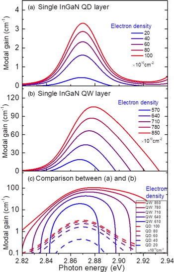
Fig. 2. (Color online) Modal gain spectra of InGaN lasers with (a) single QD-layer and (b) single QW-layer at varying injection levels; (c) the gain spectrum comparison between a QD-layer and a QW-layer in log scale.
Download figure:
Standard image High-resolution imageFigure 3 shows the dependence of peak modal gains on radiative current densities for multi-active-layer lasers. The peak modal gains are taken from the maximum gain point in the gain spectra shown in Fig. 2. From Fig. 3 we see that the transparency current density (when peak modal gain Γg = 0) in QD lasers ( = 1.8 A cm−2) is 118 times lower than that in QW lasers (
 = 212 A cm−2) for the single-active-layer case.
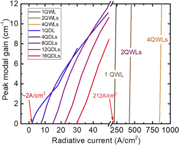
Fig. 3. (Color online) The relation of peak modal gain with current density in multi-active-layer InGaN QD lasers and InGaN QW lasers.
Download figure:
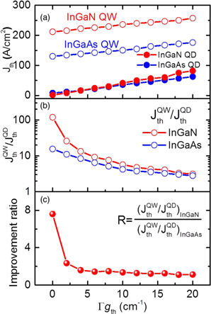
Standard image High-resolution imageBased on results shown in Fig. 3, the lasing threshold current densities Jth at different loss levels (Γgth) are calculated and shown in Fig. 4(a), with red closed-circles for InGaN QD lasers ( ) and red open circles for InGaN QW lasers (
 ). Here the numbers of active layers have been optimized to obtain the lowest Jth values. It can be seen that, within the studied loss levels (i.e., Γgth < 20 cm−1), lasers with InGaN QDs could give much lower threshold values than that with InGaN QWs. The improvement factor that is defined as
  is shown in Fig. 4(b) as red open circles, from which we can see that
  is more than 100 times lower as compared with
  at transparency condition. Even at a loss level of 20 cm−1,
  is still several times lower than
Fig. 4. (Color online) (a) The threshold current densities Jth at different loss levels in InGaN QD and QW lasers; the cases for InGaAs QD and QW lasers are also plotted as blue curves; (b) the Jth improvement of using QDs over QWs; (c) the ratio of Jth improvement from III-arsenide lasers to III-nitride lasers.
Download figure:
Standard image High-resolution image
As mentioned above, besides the effect of the lower dimensionality of QDs that results in a smaller active-region volume than QW lasers, another reason for the large improvement on  of QD lasers over QW lasers in III-nitrides would be the large effective-masses and the large asymmetry between
  and
and  In order to have a direct comparison with material systems that have relatively smaller effective-masses and smaller
  we perform similar calculations for III-arsenide lasers.
The III-arsenide laser structures are assumed to be grown on (001) GaAs templates. Being grown on a 0.5 nm thick wetting layer, In0.2Ga0.8As QDs have a truncated pyramid shape, with a top width of 6 nm, a basal width of 12 nm, a height of 2 nm and a density of  (the same as above InGaN QDs).32) These In0.2Ga0.8As QDs are capped with In0.02Ga0.98As barriers. The thickness of the corresponding In0.2Ga0.8As/In0.02Ga0.98As QWs is set as 2.8 nm to have the same ground-state transition energy (1.35 eV) as In0.2Ga0.8As QDs. A 2-μm-wide ridge structure is used with a 360 nm thick waveguiding layer, in which 10 periods of active layers are embedded with a period length of 30 nm.
The calculated threshold current densities of InGaAs lasers are also shown in Fig. 4(a) as blue circles. It is seen that the Jth of InGaAs QW lasers [blue open circles in Fig. 4(a)] is about 2 times lower than InGaN QW lasers [red open circles in Fig. 4(a)] for a fixed loss level, which is due to the smaller effective-masses and smaller effective-mass asymmetry ( ) in III-arsenide compared with those in III-nitrides, i.e.,
  III-arsenide <
  III-nitride.21) However, the Jth of QD lasers in InGaN and InGaAs looks quite similar to each other, as the influence of different effective-masses has been suppressed or eliminated by the strong quantum confinement in QDs. As a result, the threshold improvement
  from QW lasers to QD lasers in III-nitrides is larger than in III-arsenide, as shown in Fig. 4(b). For example, at transparency conditions, the improvement with InGaN is 118 times while it is only 15 times with InGaAs, which means using InGaN QDs could be 8 times more efficient than InGaAs QDs [Fig. 4(c)]. Furthermore, the reduced injection carrier density within InGaN QD lasers will in turn suppress carrier leakages and other non-radiative recombinations such as Auger recombination. These results reveal that using QDs in III-nitride lasers for low threshold applications is more advantageous than in other material systems.
5. Conclusions
In summary, we theoretically investigated the threshold current densities of III-nitride lasers with QDs and QWs in a comprehensive theoretical picture. It was found that using QDs instead of QWs for III-nitride lasers could give a large improvement on threshold current densities. At transparency condition, the improvement in III-nitride lasers could be 118 times, which, however, is only 15 times with III-arsenide. This is mainly due to the large effective-masses of carriers ( and
and  ) and the large asymmetry between the effective-masses in valence bands and conduction bands (
 ) in III-nitrides. Our results emphasize the importance of using QDs in III-nitride for low threshold laser applications, which could be 8 times more efficient than in III-arsenide.
Acknowledgments
The authors thank Satoshi Iwamoto, Toshio Saito, Munetaka Arita and Teruhisa Kotani for discussions. This work was partly supported by the Grant-in-Aid for Specially Promoted Research (15H05700) and was also based on a project commissioned by the New Energy and Industrial Technology Development Organization (NEDO).