

Abstract
Strain states in face-to-face-annealed sputter-deposited c-plane AlN (FFA-sp-AlN) films on c- and a-plane sapphire substrates were evaluated. As a result, an existence of anisotropic strain in the c-plane FFA-sp-AlN film on a-plane sapphire was ascertained by X-ray diffraction reciprocal space maps. Consequently, the peak splitting of polarized Raman spectra was observed from the c-plane FFA-sp-AlN film on a-plane sapphire for the first time. Meanwhile, there was no peak splitting of polarized Raman spectra of the c-plane FFA-sp-AlN film on c-plane sapphire, which has anisotropic strain. In addition, local and anisotropic strain relaxations in patterned FFA-sp-AlN films on c-plane sapphires were experimentally proven by polarized Raman spectra and two dimensional Raman spectra maps.
Export citation and abstract BibTeX RIS
1. Introduction
It is important to comprehend the strain state of AlN layers, since strained layers possibly change optical polarization selection rule of AlxGa1−xN light emitting devices. Especially, deep ultraviolet-light emitting diodes in UVC region is well known to have either TM- and/or TE-polarized emissions, and that strongly depends on not only AlN molar fraction of AlxGa1−xN but also strain state.1,2) However, there are very limited studies about strain states of high-quality AlN films on sapphire and/or SiC substrates,3,4) while a number of results about strains in GaN have been reported.5–13) This reason might be not sufficient crystalline quality of the AlN film on a sapphire substrate. In the case of the parameter set for AlN such as phonon deformation potentials (PDPs), there are already seeming to reliable Raman scattering studies of AlN single crystals14,15) and the high-quality AlN film on SiC.3)
We have reported a fabrication of high-quality AlN films by combining the sputtering and face-to-face thermal annealing (FFA).16–20) Recently, the large compressive strain of c-plane FFA sputter-deposited AlN (FFA-sp-AlN) films on c-plane sapphires has been observed by X-ray diffraction (XRD).18) Nevertheless, quantitative analysis of Raman scattering measurement has not yet been performed. In this study, by using Raman scattering spectroscopy in conjunction with XRD reciprocal space maps (XRD-RSMs), strain states of c-plane FFA-sp-AlN film on c- and a-plane sapphire, and patterned c-plane FFA-sp-AlN film on c-plane sapphire were evaluated.
2. Experimental methods
2.1. Sample preparations
Samples described in this paper are schematically illustrated in Figs. 1(a)–1(c). Three kinds of samples were prepared by sputtering of AlN films on c- and a-plane sapphire substrates. AlN films were deposited by RF sputtering with a sintered AlN target. During the deposition of sputtering, the substrate temperature, RF power, and Ar/N2 gas flow ratio were kept constant at 600 °C, 700 W, and 1/4, respectively. Subsequently, the FFA was conducted at 1700 °C for 3 h in N2 atmosphere.16) Finally, homoepitaxial growth of AlN on the FFA-sp-AlN film was performed by metalorganic vapor phase epitaxy (MOVPE). Trimethylaluminum and ammonia were used as the Al and N precursors, respectively. The MOVPE growth temperature and reactor pressure were maintained at 1300 °C and 30 Torr, respectively. In addition to c-plane AlN on c-plane sapphire, c-plane FFA-sp-AlN film was fabricated on a-plane sapphire substrate with same sputtering and FFA condition as c-plane sapphire, but without MOVPE growth. To investigate structure effects for local and anisotropic strain distributions, patterned AlN films on c-plane sapphire substrates were fabricated by photolithography and reactive ion etching.
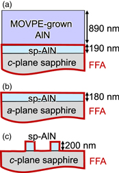
Fig. 1. (Color online) Schematics of the c-plane FFA-sp-AlN films on (a) c-plane sapphire and (b) a-plane sapphire, and (c) the patterned c-plane FFA-sp-AlN film on c-plane sapphire.
Download figure:
Standard image High-resolution image2.2. Raman scattering spectroscopy and XRD-RSMs
Strain states were evaluated by means of Raman scattering spectroscopy and XRD-RSMs. Polarized micro Raman spectra of c-plane FFA-sp-AlN films were measured with the backscattering geometry of Z(XX) and Z(YY)
 which were parallel to AlN[11–20] and [1–100], respectively. All the Raman measurements were performed using a confocal Raman microscope at room temperature (RT). The 532 nm line of the DPSS laser was used for excitation and was focused below 1 μm by an objective lens with a magnification of 100 times and a high numerical aperture of 0.9. Laser power was set to around 40 mW. This value is even lower than that in the previous study (∼150 mW), in which dislocations in GaN are detected by Raman frequency shifts.21) In addition, we should note that there were no Raman frequency shifts by illumination. Thus, this laser power was low enough to avoid heating of the sample, which causes Raman frequency shifts.8,14) Raman spectra was dispersed with a 50 cm focal length spectrometer equipped with a grating of 2400 grooves mm−1 and detected with a charge coupled device.
In the equibiaxially strained case of an AlN c-plane growth, a Raman shift Δω is derived as

where α and β are PDPs, C13 and C33 are elastic stiffness constants for AlN, and εZZ is strains along c-direction, respectively. εZZ can be discribed as

where cfilm and cbulk are film- and bulk-lattice constants along c-direction. By substituting Eq. (1) to (2), cfilm can be derived. The parameter set3,15,22–25) used in this study are listed in Table I. PDPs used in this study for  and
and  was experimentally determined from AlN bulk crystals. In addition, the elastic stiffness constants used in this study24) is well agree with results from free exciton transition energies with uniaxial pressure in AlN bulk crystal.26) To get accurate Δω value from our measurement setup, all Raman spectra of AlN on sapphire substrate were calibrated by Raman peak shift of sapphire Eg of 576.7 cm−1,27) and the bulk AlN crystal grown by the physical vapor transport method was used as a reference, i.e., strain free AlN phonon frequencies for
 and A1(LO) peaks in our setup.
Table I. PDPs, elastic stiffness constant and c lattice constant used in this study.

|

|
A1(LO) | |
|---|---|---|---|
| α (cm−1) | 1083,15,22) | −11453,15,22) | −73923) |
| β (cm−1) | −2373,15,22) | −10233,15,22) | −73723) |
| C13 (GPa) | 9524) | ||
| C33 (GPa) | 40224) | ||
| cbulk (Å) | 4.980825) |
In addition to Raman scattering measurements, XRD-RSM measurements were performed to get the macroscopic strain using Cu Kα radiation (λ = 1.5406 Å). In the case of the c-plane FFA-sp-AlN film on c-plane sapphire, measurements of XRD-RSMs were employed with the X-ray incident direction of AlN m-direction. Diffraction peaks with Miller indices of AlN (10–15) and sapphire (11–2 12) were adapted. The peak position of AlN (10–15) is effected not only by lattice constants but also by the misorientation of the film. In the case of samples described in this study, the misorientation angle of the film and the off-cut angle of the substrate were identical. Thereby, followed by 2θ offset correction based on sapphire (11–2 12), to compensate the effect from the misorientation of the film, the position of AlN (10–15) was normalized by the coordinate transformation based on the position of sapphire (11–2 12), which indicates the substrate off-cut angle. As for sapphire (α-Al2O3) lattice constants, standard parameters, i.e., a = 4.758 Å and c = 12.991 Å, were used. These values are commonly used in literatures.28–30) In the case of the c-plane FFA-sp-AlN film on a-plane sapphire, in addition to XRD-RSM measurements of AlN (10–15) and sapphire (41–5 0), XRD-RSM measurements of AlN (11–24) and sapphire (22–4 3) with the X-ray incident direction of AlN a-direction were performed to unambiguously obtain three lattice constants from a film with an anisotropic strain. These methods have already been utilized to get anisotropic strains in the case of semipolar growths of nitride semiconductors such as InGaN31) and AlInN.32)
3. Results and discussion
3.1. c-plane AlN film/c-plane sapphire
Figures 2(a)–2(c) show Raman spectra of Z(Y-) for
for 
 and A1(LO) from the c-plane FFA-sp-AlN film on c-plane sapphire. Red lines are obtained from the c-plane FFA-sp-AlN film on c-plane sapphire, and black lines are bulk AlN results observed from the exactly same Raman measurement setup. Intensities were normalized by
  peak intensities for each sample. The XRD-RSM around AlN (10–1 5) and sapphire (11–2 12) of the c-plane FFA-sp-AlN film on c-plane sapphire is shown in Figs. 3(a) and 3(b), respectively. Based on sapphire (11–2 12) position: −0.4204 rlu for qa and 0.9234 rlu for qc, AlN (10–1 5) position qm and qc were transformed from −0.3727 and 1.002 rlu to −0.3726 and 1.002 rlu, respectively. Observed values are summarized in the Table II with those obtained from XRD-RSMs. εZZ and cfilm were calculated from Eqs. (1) and (2) by substituting obtained Raman shift Δω.
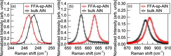
Fig. 2. (Color online) Raman spectra of Z(Y-) for (a)
  (b)
(b)  and (c) A1(LO) from the c-plane FFA-sp-AlN film on c-plane sapphire (red line) and bulk AlN substrate (black line).
Download figure:
Standard image High-resolution image
Fig. 3. (Color online) XRD-RSMs around (a) AlN (10–1 5) and (b) sapphire (11–2 12) of the c-plane FFA-sp-AlN film on c-plane sapphire.
Download figure:
Standard image High-resolution imageTable II. Obtained results from the c-plane FFA-sp-AlN film on c-plane sapphire.

|

|
A1 (LO) | XRD-RSM | |
|---|---|---|---|---|
| Raman shift (cm−1) | 246.6 | 663.1 | 892.2 | — |
| Δω (cm−1) | −0.8 | +6.6 | +4.0 | — |
| εZZ (%) | 0.12 | 0.17 | 0.17 | 0.19 |
| cfilm (Å) | 4.987 | 4.989 | 4.989 | 4.990 |
From Table II, the lattice constant c obtained from  peak well agrees with that from the XRD-RSMs. This indicates that the parameter set that shown in Table II is quite accurate especially for
  PDPs. In the same time, these results imply that the c-plane FFA-sp-AlN film on c-plane sapphire shown here has high crystalline quality, which phonon characteristics are comparable with those of bulk AlN crystals and the AlN film on a SiC substrate.3,15,22) It is worthy to note that the FWHM values of XRD rocking curves (XRC-FWHM values) of the sample are 15 and 240 arcsec for AlN (0002) and (10–12) diffractions, respectively. The values of εZZ calculate from
  and A1(LO) are quite agreed with each other even without consideration of a coupling with plasmon mode for A1(LO). Secondary ion mass spectroscopy measurements revealed that oxygen and silicon concentration for the MOVPE-grown AlN film on the c-plane FFA-sp-AlN template were 6 × 10¹⁶ and 5 × 1015 cm-3, respectively. These impurity concentrations are too low to couple with plasmon mode, and that is why there is no effect of coupling with plasmon mode for Al(LO) peak shift. This is same as the reported result of the AlN film on a SiC substrate.3) These results given above show a validity of parameter sets in this study, i.e., PDPs, elastic stiffness constants, and c lattice constant of bulk AlN shown in Table I. Hereafter, we will focus on analysis of an
  Raman peak shift, which has larger PDPs.
3.2. c-plane AlN film/a-plane sapphire
Raman and XRD-RSM measurements were performed for the c-plane FFA-sp-AlN film on an a-plane sapphire substrate. From XRD phi-scan measurement results, the epitaxial relationship of this sample was ascertained as schematically illustrated in Fig. 4(a). This epitaxial relationship is different from the sample grown by MOVPE33) and HVPE at higher temperature (1450 °C–1550 °C),34,35) and same as the samples grown by HVPE at lower temperature (700 °C).34) Comparing with above mentioned literature, it can be speculated that the epitaxial relationship of this sample ascribes the sputtering temperature (600 °C). For the 180 nm thick c-plane FFA-sp-AlN film on a-plane sapphire, XRC-FWHM values of AlN (0002) and (10–12) are 18 and 425 arcsec, respectively. The crystalline quality of the sample on a-plane sapphire is slightly inferior to that on c-plane sapphire. Nevertheless, these values indicate better crystalline (smaller XRC-FWHM values) than previous reports,33) which was grown by MOVPE. Additionally, above shown XRC-FWHM values of this sample are even smaller than that of c-plane GaN films on a-plane sapphires.36–38) Therefore, the crystalline quality of the c-plane FFA-sp-AlN film on a-plane sapphire regards as high enough to discuss the strain relaxation. Note that the optimization of fabrication conditions of c-plane FFA-sp-AlN films on a-plane sapphires is beyond the scope of this paper and will be discussed elsewhere. The XRD-RSM around AlN (10–1 5) and (41–5 0), and AlN (11–2 4) and sapphire (22–4 3) of the c-plane FFA-sp-AlN film on a-plane sapphire is shown in Figs. 5(a)–5(d), respectively. After coordinate transformation based on sapphire positions, AlN lattice constants toward a-, and m- were calculated to be 3.095 and 3099 Å. Note that the lattice constants along c-axis derived from two different Miller indices AlN (10–1 5) and (11–2 4) were almost identical: 4.991 and 4.992 Å. This coincidence indicates validity of the coordinate transformation in XRD-RSMs. Then, εxx, εYY, and εzz, (strain toward a-, m-, and c-direction of AlN) were obtained to be −0.52%, −0.41%, and 0.22%, respectively. These values clearly indicate the in-plane anisotropic compressive strain. The origin of this anisotropy might be in-plane anisotropy of the underlying substrate. In the literature the thermal expansion coefficients of sapphire c- and a-direction are reported as 8.11 × 10⁻⁶ and 7.28 × 10⁻⁶ K−1, and both values are larger than that of AlN (5.27 × 10⁻⁶ K−1 for a-direction).39) Therefore, the anisotropic strain in the c-plane AlN film on a-plane sapphire might be caused by the anisotropy of the thermal expansion coefficient of sapphire during cooling down from annealing temperature of 1700 °C to RT.

Fig. 4. (Color online) (a) Schematic epitaxial relationship of c-plane FFA-sp-AlN film on a-plane sapphire. (b) Polarized Raman spectra of c-plane FFA-sp-AlN film on a-plane sapphire. (c) Polarized Raman spectra around AlN  peaks of c-plane FFA-sp-AlN film on c- and a-plane sapphire.
Download figure:
Standard image High-resolution image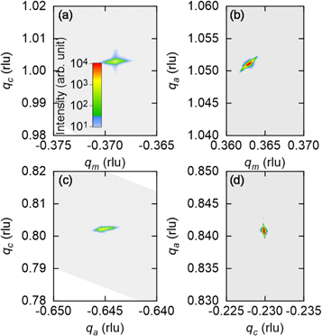
Fig. 5. (Color online) XRD-RSMs around (a) AlN (10–1 5), (b) sapphire (4 1–5 0), (c) AlN (11–2 4), and (d) sapphire (22–4 3) of the c-plane FFA-sp-AlN film on a-plane sapphire.
Download figure:
Standard image High-resolution imagePolarized Raman spectra of the sample with configurations of Z(XX) and Z(YY)
 are shown in Figs. 4(b), 4(c). As it has been reported,40) sapphire A1g peak appeared when the polarization is parallel to sapphire c-direction (Z(XX)
 ). Polarized Raman spectra of c-plane AlN on a-plane sapphire around AlN
  peaks are shown in Fig. 4(c) with those on c-plane sapphire for the comparative study. In the case of c-plane AlN on a-plane sapphire,
  frequency is slightly different between two polarization directions, while there is no difference in c-plane AlN on c-plane sapphire. This difference is very small, but it should be noted that the results are reproducible. In addition, same phenomenon has been observed in c-plane GaN on a-plane sapphire and that frequency difference was also below 1 cm−1.7) Although quantitative understanding has not been completed, we could know that the anisotropy of strain could be observed by not only from XRD-RSMs but also from polarized Raman spectra.
3.3. Patterned c-plane AlN film/c-plane sapphire
Figures 6(a) and 6(b) show the optical microscope image and correspondent one dimensional Raman spectra contour map of Z(Y-) of which x-and y-axis are Raman shift and sample position, respectively. AlN
  peaks only exist at AlN locations. Meanwhile, sapphire Eg peaks are observed from all points. To show local and anisotropic Raman peak shift clearly, Raman spectra from the patterned AlN center and edge points, and polarized Raman spectra observed at the edge point are shown in Figs. 6(c) and 6(d), respectively. As shown in Fig. 6(c), shorter frequency peak was observed remarkably at the edge point. This indicates the local strain relaxation. Moreover, polarized spectra observed at the edge shows the frequency difference, as shown in Fig. 6(d). Lower-frequency peak was observed when the polarization is perpendicular to stripe. Therefore, Raman peak at the edge point of the patterned AlN film shows local and anisotropic strain relaxation.
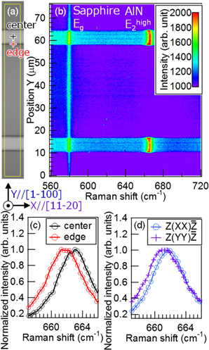
Fig. 6. (Color online) (a) Optical microscope image and (b) correspondent one dimensional Raman spectra intensity contour map of Z(Y-) of the patterned c-plane FFA-sp-AlN film on c-plane sapphire. (c)
  Raman spectra of Z(Y-)
 observed at center and edge of the AlN film. (d) Polarized
  Raman spectra of Z(XX)
 and Z(YY)
 observed at edge of the AlN film.
Download figure:
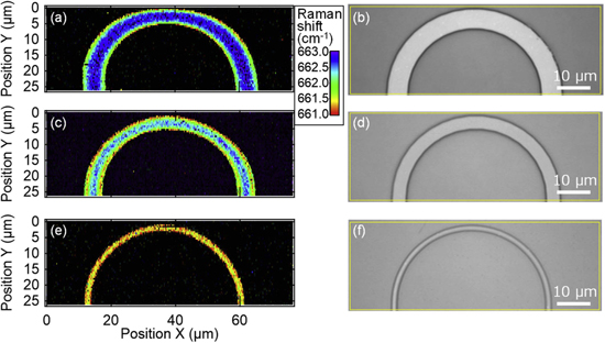
Standard image High-resolution imageTo know the AlN  peak shift distribution, two dimensional (2D) Raman
  shift maps were made by 2D Raman spectra measurements of patterned AlN films with width of 7, 5, and 2 μm and Lorentzian fitting of all points, as shown in Figs. 7(a), 7(c), and 7(e), respectively. Optical microscope images of the measurement positions of Figs. 7(a), 7(c), and 7(e) are shown in Figs. 7(b), 7(d), and 7(f), respectively. From Figs. 7(a) and 7(c) (patterned AlN films with width of 7 and 5 μm), lower-frequency peak is clearly seen at the edge point of the patterned AlN films. This indicates local strain relaxation at the edge point. It should be mentioned that peak frequencies at the center of 5 and 2 μm width samples are different from that of the 7 μm width sample. From these results, occurrence of strain relaxation not only at the edge but also at center could be observed. These kind of strain distributions have been observed from cantilevers of GaN41) and AlN.42)
Fig. 7. (Color online) 2D Raman  shift maps and correspondent optical microscope images of patterned c-plane AlN films with width of (a), (b) 7 μm, (c), (d) 5 μm, and (e), (f) 2 μm.
Download figure:
Standard image High-resolution image
4. Conclusions
By using appropriate parameters, lattice constant c obtained from Raman spectra of the c-plane FFA-sp-AlN film on c-plane sapphire are in quantitative agreement with those from XRD-RSMs. In the case of the c-plane FFA-sp-AlN on a-plane sapphire, there was a splitting of AlN  peaks in polarized Raman spectra, which was ascribed to an existence of anisotropic strain. This result qualitatively is in agreement with the results of XRD-RSM measurements. The splitting of an AlN
  phonon under anisotropic strain at the edge of the patterned c-plane FFA-sp-AlN film on c-plane sapphire substrate has also been observed. This result indicates that the anisotropic strain can be induced from anisotropies of not only substrates but also structures fabricated after the growth. As an outlook, these local and anisotropic strain relaxation might effect for nano and micro structured device performance.
Acknowledgments
The authors would like to thank Mr. S. Kawai and Mr. K. Fujikawa for sample preparations. This work was partially supported by "Program for Building Regional Innovation Ecosystems", "Program for research and development of next-generation semiconductor to realize energy-saving society", "Nanotechnology Platform Program" of MEXT, JSPS KAKENHI Grants (JP16H06415, JP17H06762), JST CREST (16815710), JST SICORP EU H2020 No. 720527 (InRel-NPower), JST SICORP with MOST in China, and the Consortium for GaN Research and Applications.