Abstract
Multilayer graphene was synthesized by overlayer growth of graphene on a monolayer graphene template using a chemical vapor deposition method under a high process temperature of 1300 °C. Structural analysis using Raman spectra revealed that the synthesized multilayer graphene forms highly crystalline graphene layers with a turbostratic stacking structure. Atomic force microscope images indicated that the step edges of the grown graphene layer proceed via lateral growth mode. The electrical transport properties of the synthesized multilayer graphene showed higher conductivity and carrier mobility than those of the monolayer graphene template. The improvement of the electrical transport properties is caused by the turbostratic stacking structure that has the electronic band dispersion similar to that of monolayer graphene. This result means that the synthesis of graphene layers grown on the graphene template is effective to improve the carrier transport properties in multilayer graphene sheets.
Export citation and abstract BibTeX RIS
1. Introduction
Monolayer graphene characterized by a linear dispersion in the band structure has been attracting considerable attention because of its excellent electrical properties.1) Such potential applications as field-effect transistors,2,3) flexible electrodes4) and battery materials5) have become important targets for many researchers around the world.
The electrical transport properties of the monolayer graphene are degraded by such surrounding environments as charge impurity and surface roughness on a substrate because the monolayer only has the thickness of a single carbon atom sheet. Recently, it has been reported that a screening effect in a multilayer graphene sheet with order stacking structures is effective to reduce the influence of the charge impurity.6) Moreover, the turbostratic multilayer graphene with the relatively weak interlayer coupling preserves both high mobility and conductivity,7) together with the screening effect. That is because the band structure of the turbostratic multilayer graphene shows a linear dispersion, which is similar to the monolayer graphene. Therefore, this material is a promising candidate for the application devices with a high electrical performance.
The chemical vapor deposition (CVD) growth using metal catalysis with high carbon solubility8–10) and the thermal decomposition of silicon carbides11) are commonly utilized for the synthesis of multilayer graphene sheets. In these methods, such order stacking structures as ABA- and ABC-stackings tend to be dominantly formed in the multilayer graphene sheets.12) In this case, the electrical band structure of the multilayer graphene comes close to a semi-metallic property as the number of layers increases, resulting in the disappearance of the linear dispersion.13) The fabrication method of the turbostratic multilayer graphene utilized for the device applications is limited to a multiple transfer method using monolayer graphene grown by CVD on Cu.7,14,15) It is an important subject to develop the large-area synthesis method of the turbostratic multilayer graphene via crystal growth.
In previous publication, we demonstrated that additional graphene layers are grown on a mechanically exfoliated monolayer graphene template using a CVD method with ethanol as a carbon feedstock.16,17) We also revealed that the grown graphene layers have a turbostratic stacking structure without any structural correlation between the additional graphene layers. Unfortunately, carrier mobilities of the synthesized multilayer graphene sheets are lower than that of the monolayer graphene template because the grown graphene has low crystallinity due to a relatively low growth temperature (720 °C). In this study, a high-temperature up to 1300 °C using an infrared heating furnace is utilized for the synthesis of the multilayer graphene using a Cu-CVD monolayer graphene as the growth template.
2. Experimental methods
2.1. Fabrication process of the multilayer graphene device with the van der Pauw geometry
Figure 1 shows a fabrication process of multilayer graphene devices. The pristine monolayer graphene as a growth template was synthesized by a CVD method using a Cu foil via the same process as previously reported.18) The monolayer graphene was transferred from the Cu foil onto a fused quarts substrate15) as shown in Fig. 1(a). Subsequently, the growth of graphene layers was conducted by a CVD method using the infrared radiation furnace. A typical graphene growth procedure is as follows: (1) sample was introduced into a furnace quartz tube19,20) and preheated at 600 °C for 5 min in air under atmospheric pressure to remove residual resist films used in the transferring process. (2) Sample was introduced into the infrared radiation furnace and heated up to 1300 °C for 4 min. (3) The growth of graphene on the monolayer graphene template was carried out by introducing the mixture of ethanol vapor as a carbon feedstock and Ar as a carrier gas under total pressure of 590 Pa. The flow rates of ethanol vapor and Ar gas were 0.5 and 200 standard cubic centimeters per minute, respectively. Figure 1(b) shows an optical microscope image of graphene grains after the growth. We can see a change in the contrast of the graphene grains between before and after growth in the optical images, indicating that the film thickness of the graphene grains becomes to be thicker by the thermal process. Finally, the graphene device for Hall-effect measurement was fabricated by a conventional photolithographic technique. Au (40 nm)/Ni (10 nm) as the electrode was deposited onto the graphene film. Subsequently, the unnecessary part of graphene for van der Pauw geometry was removed by plasma etching to form the square pattern as shown in Fig. 1(c).

Fig. 1. (Color online) Experiment process: (a) transferring the pristine monolayer graphene. (b) Growth of graphene and (c) device fabrication.
Download figure:
Standard image High-resolution image2.2. Structural and electrical analysis
To determine the number of grown graphene layers, Raman spectroscopy was carried out at room temperature using a laser excitation of 532 nm with a 100× objective lens (typical spot diameter: ∼1 μm). The laser power was kept at a constant value of 0.28 mW, so that the heating effects on the frequencies of the Raman signal can be ignored. The details of the evaluation method of the layer numbers from the Raman spectra are described in appendix. The surface morphology on the grown graphene layers was evaluated by atomic force microscope (AFM) observations using HITACHI AFM5100N with the dynamic force mode. Hall-effect measurements were performed under the current of 10 μA and the magnetic field of 3200 G. It should be noted that the samples tested in Raman, AFM and Hall-effect measurements are different.
3. Results and discussion
3.1. Stacking analysis of the synthesized graphene layers using Raman spectroscopy
Figure 2 shows the Raman spectra of grown graphene layers prepared by different growth time. The spectra are normalized by a peak intensity (Isub.(obs.)) from the fused quartz substrate (∼460 cm−1) as indicated by the arrow in Fig. 2.21) Three characteristic peaks can be observed in the Raman spectra: (1) the G-band (∼1580 cm−1) is caused by the double degenerate phonon mode at the Brillouin zone center. (2) The D-band (∼1350 cm−1) mode originates from the sp2-hybridized disordered carbon materials.22) (3) The two-dimensional (2D)-band is the overtone of the D-band, which is used to determine the number of layers and the stacking structures in few-layer graphene sheets.23–25) The number of grown graphene layers efficiently increases to 2, 6 and 11 layers by the thermal treatment using ethanol vapor as shown in Fig. 2(a). The intensity ratio (ID/IG) of the D-band and G-band peaks, and the full width at half maximum (FWHM; ΓD) of the D-band are evaluated to be ∼0.36 and ∼ 49 cm−1 for the 6-layer graphene. The grain size evaluated from the ID/IG is about 60 nm.25) The values of the ID/IG and ΓD are smaller than those values (ID/IG = ∼0.75, ΓD = ∼201 cm−1) observed from the multilayer graphene (4 layers) grown by a relatively low temperature (720 °C), as previously reported.17) Since these values reflect the crystallinity of graphene, this indicates that the higher process temperature is effective to improve the crystallinity of grown graphene layers.

Fig. 2. (Color online) (a) Raman spectroscopy observed from monolayer and multilayer graphene, and (b) the 2D-band that fitted by three Lorenz peaks for the evaluation of turbostratic ratio.
Download figure:
Standard image High-resolution imageThe stacking structure in multilayer graphene can be divided into two types: turbostratic and order stacking (e.g. AB stacking). The turbostratic ratios (R') of the multilayer graphene were evaluated by the peak fitting analysis in the 2D-band region.26) The peak shape in the 2D-band was fitted by three Lorenz curves with the center positions at 2680, 2700 and 2720 cm−1, as noted by IG'3DA, IG'2D and IG'3DB. The turbostratic ratio (R') can be given by

where the R means the order stacking ratio. The ratios of turbostratic stacking in grown multilayer graphene with 2, 6 and 11 layers are about 92%, 80% and 69%, which decrease with increasing the number of layers. Since the growth time increases with increasing the number of layers, it is likely that the change in the ratio of turbostratic stacking was affected by thermal annealing time.
3.2. Analysis of the surface morphology of grown graphene using AFM
Figures 3(a)–3(c) show the AFM images observed from the grown graphene surface with different film thicknesses. Figures 3(e) and 3(f) are the height profiles along L–L', M–M' and N–N' lines in each surface and the root mean square (RMS) roughness as a function of the number of layers. When the number of layers is less than 5 layers, the RMS roughness roughly corresponds to the single graphene step height (∼0.34 nm), indicating that the grown graphene forms atomically flat surfaces. Here we define the growth with the low RMS roughness less than 5 layers as an initial stage. Figure 3(d) shows an enlarged AFM image of the grown graphene islands at the initial growth stage. The graphene islands form the flat terrace structure with the single step height as indicated by the height profile along the P–P' line in Fig. 3(g). This means that the step edges of graphene islands after the nucleation proceed by the lateral growth mode [Fig. 3(h)]. The typical diameter of the 2D islands exceeds 100 nm, which is larger than the grain size (∼60 nm) evaluated from the Raman spectra. This is probably because the ID used for the evaluation of the grain size also reflects the small defects in the grown graphene islands and the domain boundaries formed by the coalescence among islands.

Fig. 3. (Color online) AFM images of graphene with (a) 2 (b) 5, and (c) 11 layers and their (e) height profiles along L–L', M–M' and N–N' lines and (f) RMS roughness evaluation. (d) Enlarged AFM image of grown graphene islands after the growth of 2 layers and (g) the height profile along P–P' line in Fig 3(d). (h) and (i) are the formation model of graphene islands when the number of grown layers is less than 5 layers and over 10 layers, respectively.
Download figure:
Standard image High-resolution imageAfter the further growth, the three-dimensional (3D) islands with extremely high height are observed as indicated by the arrows in Fig. 3(c). The center of every island tends to contain the defective structure with large roughness as compared with the flat terrace site formed by the lateral growth. The trend is enhanced by increasing the number of layers. Since the defective sites with many dangling bonds promote the incorporation of carbon species, the 3D-islands are formed by the enhancement of the local growth rate [Fig. 3(i)]. As a result, the surface roughness increases with increasing the number of layers [Fig. 3(f)].
3.3. Evaluation of electrical properties in turbostratic multilayer graphene
Figure 4 shows the dependence of the number of layers on the sheet resistance (Rs) of grown multilayer graphene measured by van der Pauw geometry. The Rs decreases with increasing the number of layers. This result means that the current flows in the grown graphene layers as the additional channels. Note that the change in the Rs is almost linear with respect to the number of layers. This indicates that the Rs of every layer in the turbostratic structure is similar to that of the pristine monolayer graphene used as the growth template. We observed that the carrier mobility (∼1280 cm2 V−1 s−1) in the grown graphene with 2 layers is higher than that obtained from the pristine monolayer graphene (∼940 cm2 V−1 s−1) at room temperature. It has been reported that the carrier mobility in the few-layer graphene with the order stacking structure degrades as compared with that in monolayer graphene,6) which is oppositely different from our grown graphene with 2 layers. The improvement of the carrier mobility is caused by the turbostratic stacking effect that kept the linear dispersion. Unfortunately, the carrier mobility obtained from the grown graphene with 6 layers showed the lower value (∼520 cm2 V−1 s−1) compared with that from the pristine graphene. This suggests that the carrier mobility decreases as the defect increases as indicated by the Raman spectrum [Fig. 2(a)]. From these results, we believe that the multilayer graphene grown on the graphene template is effective to improve the carrier transport properties in the graphene sheet.

Fig. 4. (Color online) Sheet resistance of monolayer and turbostratic multilayer graphene as a function of the number of layers.
Download figure:
Standard image High-resolution image
4. Conclusions
We examined graphene growth on a Cu-CVD monolayer graphene template using a CVD method under the high process temperature of 1300 °C. The Raman spectra exhibited that the synthesized multilayer graphene sheets form highly crystalline graphene layers with a turbostratic stacking structure, and the turbostratic ratio decreases with increasing the number of layers. The AFM data indicated the 2D graphene islands with the single step height (∼0.34 nm) are formed at an initial growth stage where the number of layers is less than 5 layers. After the further growth, the 3D islands are formed, resulting in the increasement of surface roughness. The electrical transport properties such as the sheet resistance and the carrier mobility enhance with increasing the number of layers. The improvement of the carrier transport properties is caused by the turbostratic stacking effect where the band structure of the multilayer graphene is similar to that of the monolayer graphene. This result means that the synthesized multilayer graphene has the potential to become an effective material to produce the device application with high electrical performances.
Acknowledgments
This research was supported by a Grant-in-Aid for Challenging Exploratory Research (No. 16K13639) and Grant-in-Aid for Scientific Research on Innovative Areas (No. 15H05866, 17H05336, 17H02745) from the Japan Society for the Promotion of Science (JSPS). This work was partly supported by the Ministry of Education, Culture, Sports, Science and Technology (MEXT) Photonics Advanced Research Center Program (Osaka University).
Appendix
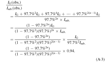
The number of layers in graphene is determined by the intensity ratio (IG(obs.)/Isub.(obs.)) of the peaks observed at the G-band region (1580 cm−1) and the substrate (460 cm−1) in the Raman spectra, assuming that the laser power decreases by 2.3% through the monolayer graphene layer due to the self-absorption effect.27) Then, the IG(obs.)/Isub.(obs.) observed from the monolayer graphene can be described by the following equation
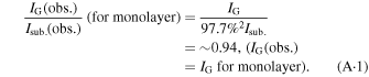
Here IG and Isub. mean the intrinsic peak intensities of the monolayer graphene and the substrate without the absorption effect. The value (∼0.94) of the IG(obs.)/Isub.(obs.) for monolayer can be evaluated from the Raman spectrum in the pristine graphene [lower part in Fig. 2(a)]. We consider that the Isub.(obs.) decreases with increasing the number of graphene layers due to the absorption effect as shown by the following equation

Finally, the IG (obs.)/Isub.(obs.) for the n-layers graphene should be expressed as