

Abstract
A 3D kinetic Monte-Carlo simulator is developed to evaluate the degradation and time-dependent variability of the device subjected to arbitrary bias conditions, which is validated by experimental results. The multi-trap including interface states and bulk traps induced reliability degradation is investigated based on trap behaviors simulation in a unified framework. Utilizing the proposed method, threshold voltage shift (ΔVth) and the variability in the nanosheet nFETs with HfO2 gate dielectric under over the full bias space are simulated. The time evolution of the stress-induced interface/bulk trap number, as well as the respective contribution to the degradation, can be distinguished under different Vg/Vd bias combinations. Simulation results show that hot carrier injection induces more serious ΔVth and suffers more variation due to the dominant contribution of interface states. Moreover, the ΔVth induced by bias temperature instability is more prominent than that under off-state stress at 398 K.
Export citation and abstract BibTeX RIS
1. Introduction
Time-dependent reliability and variability, such as bias temperature instability (BTI), hot carrier injection (HCI), threaten significantly the safe operating window and lifetime of the advanced transistors with ultra-scaled dimensions.1–4) The devices in different application scenarios may undergo a wide range of Vg/Vd bias combinations, especially in analog circuits.5,6) Therefore, the limited set of bias combinations in the measurements or separate simulations of BTI and HCI induced degradation might lead to an insufficient lifetime prediction for the normal operating devices.7,8) Moreover, the quantitative contribution of interface states and bulk traps to the degradation and variability under different bias combinations are difficult to distinguish from measurements.9,10) Multiple reliability issues co-interacting strongly with each other during circuit operation are associated with the multi-trap behaviors in the gate dielectrics.11–17) Hence, the physics-based trap behaviors simulation is essential for comprehending degradation and tracing the corresponding variability stressed by arbitrary Vg/Vd bias combinations.
In this work, the 3D kinetic Monte-Carlo (KMC) simulator including multi-trap microscopic physical mechanisms in a unified system is developed to capture degradation and variability over the full bias space. The developed simulator is verified by experimental results under different stress modes. Utilizing the simulator, the degradation induced by multiple traps under three stress modes are compared. The mapping of threshold voltage degradation (ΔVth) in nanosheet (NS) nFETs with HfO2 gate dielectric is also performed. The extended works compared to the content in Ref. 18 include the detailed descriptions of the reliability modeling, the difference of the temperature dependent degradation between BTI and off-state stress (OSS), as well as the mapping of the interface state contribution to the total degradation. Furthermore, the statistical average impact of a single defect on the ΔVth is identified from the simulation results.
2. Simulation framework and device structure
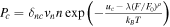
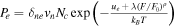
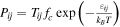
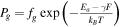
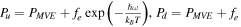
Fully-coupled physical mechanisms for multiple traps are illustrated in Fig. 1. The traps simulated in this work are interface states between the channel and interfacial layer (IL) together with the bulk traps located in the IL, high-k layer (HL) and the IL/HL interface. The defect behaviors in gate dielectrics simulated by the 3D KMC method can be categorized as follows: the charge trapping/detrapping, the generation/recombination of interface/bulk traps and trap interaction. The multi-physical processes are dependent on the electrical field, carrier energy and temperature. The detailed equations used in the 3D KMC simulator are listed in Table I. The trapping and detrapping probabilities obey the nonradiative multi-phonon theory, which can be calculated as Eqs. (1)–(3).19–21) The generation and recombination of bulk traps follow the chemical reaction model using Eqs. (4) and (5).22,23) The breakage and passivation of Si-H bonds are regarded as the generation and recombination of interface states, which are described with the truncated harmonic oscillator model according to Eqs. (6)–(11).24–26) The occurrence of each event is determined by the probabilities during every time step. The integrated simulation flowchart for the evaluation of degradation under arbitrary bias conditions is shown in Fig. 2. For a given device structure and the stress condition, the input of 3D-electric field, potential, carrier density and energy distribution can be obtained from the device simulator. The pre-existing oxide traps are distributed randomly in the gate dielectric on the basis of the initial defect density. Besides, the values of model parameters mainly depending on the atomic nature of defects are set in reasonable ranges according to the theoretical calculations and experimental findings.27–30) The final output results such as threshold voltage shift and its variation are the statistics of charged traps over time. Figure 3 shows the simulation of PBTI effect under different Vg biases, exhibiting excellent agreement with experiments.31) And the simulation of HCI degradation in HfO2 based nFinFETs under Vg/Vd 2.0 V/2.0 V bias also fits well with measured data.32) Therefore, the simulator is capable of evaluating reliability under different degradation modes in the unified framework.
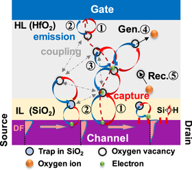
Fig. 1. (Color online) Defect activities including interface traps and bulk traps in the gate dielectric are simulated by the 3D KMC method. (1) Trapping from channel/gate; (2) detrapping to channel/gate; (3) tunneling between two traps, i.e. trap interaction; (4) trap generation; (5) trap recombination.
Download figure:
Standard image High-resolution imageTable I. Modeling equations for reliability prediction over the full bias space.
| Probabilities for trap behaviors in the gate dielectrics | |
|---|---|
|
(1) |
|
(2) |
|
(3) |
|
(4) |
|
(5) |
|
(6) |
|
(7) |
|
(8) |
|
(9) |
|
(10) |
|
(11) |
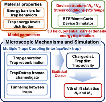
Fig. 2. (Color online) 3D KMC simulation flowchart for the evaluation of trap-induced degradation under arbitrary bias conditions.
Download figure:
Standard image High-resolution image
Fig. 3. (Color online) (a) Comparison of Vth shift under PBTI stress between the 3D KMC simulation and experimental data. (b) Comparison of experimental result and IdVg curve simulated by TCAD (c) HCI degradation simulated by the 3D KMC method compared to experiment under the condition of Vg = Vd = 2 V.
Download figure:
Standard image High-resolution imageThe three-layer stacked NS nFET with 12 nm gate length is simulated in this work, as shown in Fig. 4. In addition, 0.4 nm thickness SiO2 and 3.6 nm thickness HfO2 are applied to the gate-stacks. The initial defect densities in IL, HL and the IL/channel interface are about 1018 cm−3, 5 × 1018 cm−3, and 1011 cm−2, respectively. The following investigation of reliability degradation in the NS nFET under different Vg/Vd bias combinations is carried out on 200 samples using a set of model parameters listed in Table II.

Fig. 4. (Color online) Schematic of three-layer horizontally stacked nanosheet structure used in this work. The gate dielectrics consists of 0.4 nm thickness interfacial layer (IL) and 3.6 nm thickness high-k layer (HL).
Download figure:
Standard image High-resolution imageTable II. Model parameters used in the 3D-KMC simulation.
| Para. | HL | Para. | HL | IL |
|---|---|---|---|---|
| Ea0 | 2.55 eV | uc0 | 0.77 eV | 0.6 eV |
| Er0 | 1.1 eV | ue0 | 0.47 eV | 0.55 eV |
| σEa | 0.36 eV | σc | 0.16 eV | 0.2 eV |
| σEr | 0.2 eV | σe | 0.1 eV | 0.1 eV |
| γ | 0.85 nm | ρ | 1.5 | 1 |
| uc,e | N(uc0,e0, σc,e) | λ | 0.05 eV | 0.04 eV |
| Ea,r | N(Ea0,r0, σEa,Er) | F0 | 102 V cm−1 | 102 V cm−1 |
| Interface |
 ω ω |
p | Eb | fe |
| Para. value | 0.075 eV | 11 | 1.5 eV | 0.1 ps−1 |
3. Results and discussion
The time evolution of trap distributions in the gate dielectric of the NS nFET under the HCI mode is illustrated in Fig. 5. It can be seen that both charged interface states and bulk traps are involved in the degradation. Furthermore, the more charged interface states are generated than bulk traps and mostly located near the drain side due to the larger bond-dissociation probability. Figures 6(a) and 6(b) show the statistical average number of interface states and bulk traps over time under three typical degradation modes, respectively. It can be noted that the number of interface states is maximum in HCI mode (Vg/Vd 1.5 V/1.5V) while bulk traps contribute the most in the degradation induced by BTI stress (Vg/Vd 1.5V/0V). Further statistics of charged traps in Fig. 6(c) show that ΔVth induced by HCI and OSS (Vg/Vd 0 V/1.5 V) are severer than BTI mode even though more bulk traps are generated under BTI stress. Cumulative distributions of ΔVth after 100 s BTI, HCI and OSS are plotted in Fig. 7(a) and the variations of ΔVth are shown in Fig. 7(b). The results indicate that the maximum ΔVth variation appears in HCI mode, and BTI degradation exhibits the smallest ΔVth variation. It also should be noted that the ΔVth variability depends on the dimensional parameters of NS structure. The larger ΔVth variation can be observed in the NS FETs with the reduced gate width or thickness of NS due to the decreased device gate area.33) Particularly, the gate oxide along the width direction plays a dominant role in the reliability of NS FETs with thin thickness because of the higher average oxide electric field and the larger trapping area.
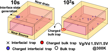
Fig. 5. (Color online) The trap distributions including interface states and bulk traps in the gate dielectric of a layer nanosheet under Vg/Vd 1.5 V/1.5 V stress at 10 s and 100 s, respectively. Time evolution of trap generation and charge are also shown.
Download figure:
Standard image High-resolution image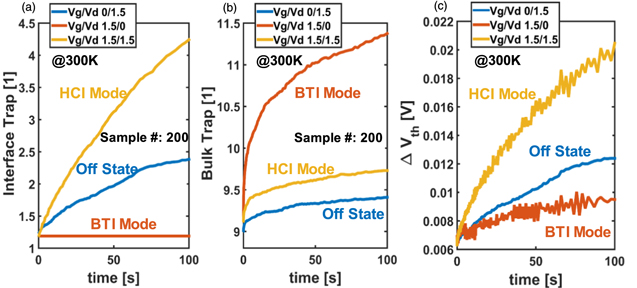
Fig. 6. (Color online) Statistical average: (a) interface trap number and (b) bulk trap number over time under three different stress conditions, (c) Vth shift under three stress modes.
Download figure:
Standard image High-resolution image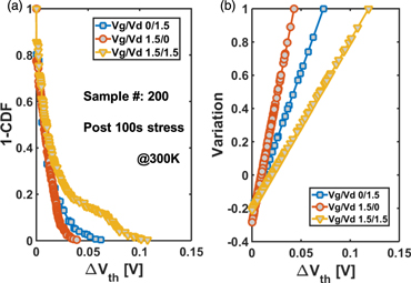
Fig. 7. (Color online) (a) Cumulative distribution and (b) variation of ΔVth after 100 s stress under three degradation modes.
Download figure:
Standard image High-resolution imageTo comprehend the reasons behind the degradation difference under varying bias combinations, the statistical average impact of a single charged trap on the threshold voltage (η) is extracted from simulation results. The parameter η acts as an indicator of the variability and also provides the crucial link between statistical modeling and measurements in the deeply scaled technologies.34) It can be observed in Fig. 8(a) that the peak value of η reaches 4.5 mV under the most serious HCI case (i.e. Vg = Vd = 1.5 V) followed by the OSS mode, whereas η for the BTI mode remains below ∼1.0 mV. A clear increase of η can be seen in the zone where Vd is above ∼0.5 mV due to the increased generation of interface states. What's more, η increases slightly when Vg moves to 1.5 V for the pure BTI condition (Vd = 0 V). The mapping of the interface state contribution also can be obtained from the 3D KMC simulations, as shown in Fig. 8(b). Here, the ratio of interface state induced degradation to the total statistical average degradation ζit is expressed as follows
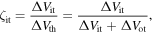
where ΔVit and ΔVot are two components in the ΔVth induced by interface states and bulk traps, respectively. It can be found that the mean contribution of charged interface states to the total ΔVth is up to ∼83% and occurs at Vg = Vd = 1.5 V condition. However, ζit is under 20% for the regimes of weak Vd and pure BTI due to the more bulk traps generated away from the channel/IL interface. Also indicated in Fig. 8, the ζit map shows that the bias condition of the peak is identical to that of η over the full bias space, and the trend of ζit is similar to η above the pinch-off region (Vg − Vth = Vd). Thus, the charged trap locations have the dominant effect on η. Moreover, the larger η indicates that the majority of charged traps are generated near the channel/IL interface. The mappings of ΔVth of NS nFETs after 100 s stress under different temperatures are presented in Figs. 9(a) and 9(b), respectively. The simulated results show that the highest ΔVth is induced by HCI stress for both the temperatures of 300 and 398 K because of the dominant interface state contribution. The worst-case degradations in the ΔVth mappings are equal to 22 mV and 142 mV, respectively. However, high temperature leads to a visible degradation increase under BTI stress compared to that for OSS mode, indicating that ΔVth caused by BTI is severer than that induced by OSS mode at 398 K. The phenomena can be attributed to the different temperature dependence of degradation mechanisms and respective trap components.
Fig. 8. (Color online) Statistical average: (a) the impact of a single charged trap on ΔVth and (b) the contribution of charged interfacial trap to ΔVth over the full bias space after 100 s stress.
Download figure:
Standard image High-resolution image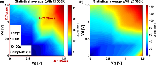
Fig. 9. (Color online) Mapping of Vth degradation in nanosheet nFETs over the full bias space after 100 s stress under (a) 300 K and (b) 398 K conditions.
Download figure:
Standard image High-resolution image
4. Conclusions
The 3D KMC simulator featuring a unified system of multi-trap behaviors in the gate dielectrics is developed for investigating reliability and variability of the device under arbitrary bias conditions. The reliability degradation together with variation in the three-layer stacked NS nFETs are simulated. The time evolution and respective contribution of stress-induced interface states and bulk traps under three typical degradation modes are presented. Moreover, the mapping of statistical average degradation and the single defect impact on the ΔVth are shown. The results indicate that ΔVth and its variation induced by HCI are serious than BTI and OSS due to the fact that the interface states play a dominant role.
Acknowledgments
This work is supported by National High-tech R&D Program (863Program) 2015AA016501 and NSFC 61674008, 61421005.