

Abstract
Resistive switching properties of hafnium oxide and manganese oxide double-layer films sandwiched between Pt bottom electrode and Ag top electrode have been investigated. The devices exhibited bipolar resistive switching. As compared with the devices with hafnium oxide and manganese oxide single layer, the double-layered devices showed better resistive switching behaviors, including forming-free behavior, a high resistance ratio (>105–6), and good retention properties. The forming-free behavior of the bilayer device is very useful for resistive random access memory applications. The high resistance ratio is beneficial to distinguish the storage information. The formation and disruption of Ag conductive filament in the oxide layers led to the resistance changes.
Export citation and abstract BibTeX RIS
1. Introduction
Conductor–insulator/semiconductor–conductor systems, which show resistive switching effects under external stimuli, have been intensively researched owing to their remarkable performance such as simple fabrication process, high packing density, low operation voltage, and high speed.1–4) Generally, the transition metal oxides, such as NiO, TiO2, Ta2O5, ZnO, ZrO2, HfO2 and MnO, have attracted increasing attention for the application in resistive switching random access memory (RRAM).4–11) Hafnium oxide has high band gap, high dielectric constant, long-term retention, and good compatibility with the CMOS technology.8,12–14) A vertical RRAM (V-RRAM) composed of double-layer stacked hafnium oxide exhibited excellent switching performance including low reset current, good endurance, and read disturbance immunity.8) Conductive filament morphology in hafnium oxide layer has been analyzed using scanning transmission electron microscopy (STEM) and electron energy loss spectroscopy.13) Manganese oxide acted as a switching element and presented excellent performance.9,15) Reversible nonpolar resistive switching behaviors with a large resistance ratio were reported in Pt/MnOx/Pt and Pt/MnOx/Al devices.9) Stable and uniform bipolar resistive switching properties have been investigated in Ti/MnO2/Pt devices and the switching effect was attributed to the formation and dissolution of the filaments composed of oxygen vacancies with nonlattice oxygen ions.15)
RRAM based on a double-layered structure is thought to have merits of stable cycling, self-rectifying resistive switching, no electroforming, and self-compliance over single-layered devices.12,16–18) The TiO2/HfO2 resistive switching devices exhibited self-rectification caused by Schottky barrier at the interface between the top electrode and TiO2 layer.12) On the basis of HfO2 and Ta2O5, HfO2 film was the resistive switching layer and Ta2O5 film acted as rectification layer. The high Schottky barrier between the top electrode and Ta2O5 contributed to the rectifying effect.16) The repeatable self-compliance caused by the discontinuity of conduction band at Ta2O5 and MnO interface was investigated in Ta2O5/MnO devices.17) High self-rectifying ratio, little cycling variation, forming-free and self-compliance behaviors were achieved in the TaOx/TiO2 double-layer V-RRAM by homogeneous barrier modulation.18)
In this study, the devices of Ag/MnOx/Pt, Ag/HfOy/Pt, and Ag/MnOx/HfOy/Pt were fabricated to compare their characteristics for resistive switching applications. Ag/MnOx/Pt devices exhibited stable resistive switching behaviors with relatively low resistance ratio (∼103). Ag/HfOy/Pt devices showed high resistance ratio with scattered resistances in high resistance state (HRS). However, those properties were considerably modified in MnOx/HfOy double-layer devices. The Ag/MnOx/HfOy/Pt devices exhibited improved bipolar resistive switching characteristics such as forming-free behavior, high resistance ratio (>105–6), and good retention properties. A large storage window (resistance ratio of the HRS to the low resistance state (LRS)) in MnOx/HfOy double-layer devices is potentially advantageous to distinguish the storage information and restrict the misreading probability in future application of resistive switching memories.19)
2. Experimental
The MnOx/HfOy double-layered resistive switching devices were fabricated on a platinum (Pt) bottom electrode by radio frequency magnetron sputtering with hafnium oxide and manganese oxide targets in Ar ambient at room temperature. Then, silver (Ag) top electrodes were deposited by thermal evaporation using a shadow mask. The diameter of the electrode was ∼100 μm. The thicknesses of the top electrode and bottom electrode were 100 nm and 150 nm, respectively. The thicknesses of MnOx and HfOy films were 16 nm. Moreover, Ag/MnOx/Pt and Ag/HfOy/Pt devices were also fabricated and the thicknesses of the single layers were 32 nm. The schematic illustrations of the devices are depicted in Fig. 1. The structure of Ag/MnOx/HfOy/Pt devices was characterized using high-resolution transmission electron microscopy (JEM-2100F (JEOL)). To further confirm the chemical composition of the double-layer device after SET process, the energy dispersive X-ray spectroscopy (EDX) profiling analysis was measured in STEM mode. The current–voltage (I–V) measurements were performed using an Agilent 4156B semiconductor parameter analyzer with a current range of ±1 pA to ±0.1 A. The voltage was applied at the Ag top electrode while the Pt bottom electrode kept grounded.

Fig. 1. (Color online) Schematic illustration of (a) Ag/MnOx/Pt devices, (b) Ag/HfOy/Pt, and (c) Ag/MnOx/HfOy/Pt devices.
Download figure:
Standard image High-resolution image3. Results and discussion
Figure 2(a) shows the typical I–V properties of the Ag/MnOx/Pt, Ag/HfOy/Pt, and Ag/MnOx/HfOy/Pt devices. Applying a positive voltage on the Ag top electrode, the three devices switched from HRS to LRS. And then, the devices changed from LRS to HRS by applying a negative voltage. The devices exhibited typical bipolar resistive switching characteristics. A high-voltage forming operation is required to activate the switching property across the insulating layers before the reversible switching performed near the electrode/oxide layer interface.20) The following applied voltage is much lower than the forming voltage. As shown in Fig. 2(a), in Ag/MnOx/Pt, Ag/HfOy/Pt and Ag/MnOx/HfOy/Pt devices, the set voltages were 0.95 V, 0.45 V, and 0.65 V, respectively. The low-voltage SET switching processes without forming operations were obtained. No forming process was needed for those devices to induce resistive switching properties. Therefore, the three kinds of devices showed forming-free behaviors which were attributed to the numerous interface states and defects in the oxide layers formed during sputtering process. At the reading voltage of +0.2 V, the resistance ratios of HRS to LRS in Ag/MnOx/Pt, Ag/HfOy/Pt, and Ag/MnOx/HfOy/Pt devices were found to be ∼3.2 × 10³, 8.21 × 10⁴, and 6.91 × 10⁵, respectively. Figure 2(b) shows the switching cycles up to 200 cycles of Ag/MnOx/Pt, Ag/HfOy/Pt, and Ag/MnOx/HfOy/Pt devices. According to this figure, the Ag/MnOx/HfOy/Pt devices exhibited high resistance ratio and stable cycle properties. Compared with Ag/HfOy/Pt devices, the stability of switching cycles was considerably improved in Ag/MnOx/HfOy/Pt devices. Compared with Ag/MnOx/Pt devices, the resistance ratio increased intensively in Ag/MnOx/HfOy/Pt devices. Even though the devices with hafnium oxide single layer have a large average resistance ratio, they presented dispersive resistances in HRS. As shown in Fig. 2(c), the cumulative probability distributions for RHRS, and RLRS were depicted at the reading voltage of +0.2 V. The Ag/MnOx/HfOy/Pt devices showed a quite narrow distribution of HRS and LRS and the distribution of HRS was observed to be within 3 orders of magnitude. The resistance switching performance of the devices with double-layer was remarkably improved compared with those of the single layer based devices. Figure 2(d) shows the typical endurance characteristics of the Ag/MnOx/HfOy/Pt devices at room temperature by electrical pulses. The resistance fluctuated between HRS and LRS by the alternative ac pulses of +3 V and −3 V with a pulse width of 50 ms. Both HRS and LRS were read out at +0.2 V. Stable HRS and LRS were achieved and a high resistance ratio (>104) was obtained. Therefore, the Ag/MnOx/HfOy/Pt devices presented good uniformity and reliability.
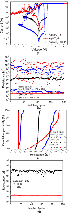
Fig. 2. (Color online) (a) I–V curves of Ag/MnOx/Pt, Ag/HfOy/Pt and Ag/MnOx/HfOy/Pt devices. (b) Resistance of HRS and LRS with respect to the sweeping cycles of Ag/MnOx/Pt, Ag/HfOy/Pt and Ag/MnOx/HfOy/Pt devices. (c) Distribution for HRS and LRS of Ag/MnOx/Pt, Ag/HfOy/Pt and Ag/MnOx/HfOy/Pt devices. (d) Endurance of Ag/MnOx/HfOy/Pt devices. The pulse voltages were ±3 V and the resistance was measured at +0.2 V. The pulse width was 50 ms.
Download figure:
Standard image High-resolution imageUnderstanding the switching mechanism is essential for device optimization.21) In order to reveal the switching behavior of Ag/MnOx/HfOy/Pt devices, the TEM and EDX analyses were performed. After several repetitive switching cycles, the devices were switched to LRS and HRS, respectively. Then the samples for TEM measurements were prepared via focused ion beam. Figure 3(a) shows the TEM image of the cross-sectional structure of the Ag/MnOx/HfOy/Pt device after SET. The thicknesses of both MnOx layer and HfOy layer were approximately 16 nm. A well-distinguishable switching layer structure composed of a crystalline MnOx layer and an amorphous HfOy layer was observed. According to Fig. 3(a), the oxide layers of the single layer devices with structures Ag/MnOx/Pt and Ag/HfOy/Pt showed a crystalline MnOx layer and an amorphous HfOy layer, respectively. However, it seems difficult to search the exact Ag conductive filaments. To further confirm the chemical composition of Ag/MnOx/HfOy/Pt device in LRS and HRS, the EDX profiling analyses were performed in STEM mode [Figs. 3(b) and 3(c)]. Figures 3(d) and 3(e) show the EDX line profile of the device under low resistance and high resistance, respectively. The region of coexistence of manganese, hafnium, and oxygen adjacent to the bottom Pt electrode was caused by the diffusion of MnOx during sputtering process. It was observed that oxygen profile was attracted towards Ag/MnOx side when the device was under low resistance, as shown in Fig. 3(d). It confirmed that the oxygen ions migrated from HfOy layer to Ag/MnOx side when a positive voltage was applied to Ag/MnOx/HfOy/Pt device. Also, some oxygen ions gathered at the Ag/MnOx interface. According to Fig. 3(e), oxygen profile was shifted to Pt bottom electrode when the device switched to HRS. It indicated the oxygen ions extraction from Ag/MnOx side to HfOy layer.22)

Fig. 3. (Color online) (a) TEM image of Ag/MnOx/HfOy/Pt device. (b) STEM image of Ag/MnOx/HfOy/Pt device under low resistance. (c) STEM image of Ag/MnOx/HfOy/Pt device under high resistance. (d) Line profile of the EDX intensity of O, Pt, Hf, Mn, and Ag elements along the white line in (b) from Ag top electrode to Pt bottom electrode. (e) Line profile of the EDX intensity of O, Pt, Hf, Mn, and Ag elements along the white line in (c) from Ag top electrode to Pt bottom electrode.
Download figure:
Standard image High-resolution imageThe resistive switching can be caused by Ag filament or by oxygen vacancies.22–26) In the scenario of oxygen vacancies, the resistive switching was ascribed to the creation and rupture of oxygen-deficient conductive filaments.25,26) However, the Ag filament plays a key role for the resistive switching phenomena in Ag-based devices. The resistive switching phenomena in Ag/MnOx/HfOy/Pt devices were attributed to the formation and annihilation of Ag conductive filament in MnOx/HfOy layers.22–24) When a positive voltage was applied to Ag top electrode, Ag atoms oxidized to Ag ions and migrated toward Pt bottom electrode under the high electric field. Then, Ag ions reduced to metallic Ag leading to the formation of Ag conductive filament. As the filament formed in oxide layers, the conductive path connected from bottom electrode to top electrode. The devices switched to LRS. Under a negative voltage, elemental Ag near Pt electrode oxidized to Ag ions and drift toward the top electrode. Then the Ag filament was dissolved and the conductive path ruptured. The devices switched to HRS. The HfOy layer was amorphous and the conductive filaments were formed and annihilated randomly. Consequently, the Ag/HfOy/Pt devices showed a considerable high variation of resistances in HRS. However, that obstacle was solved with the additional MnOx layer. When a negative voltage was applied to the top electrode, the conductive path directly ruptured. The processes of the formation and rupture of Ag filament in Ag/MnOx/HfOy/Pt devices are illustrated in Fig. 4.

Fig. 4. (Color online) Schematic illustrations of the resistive switching mechanisms in Ag/MnOx/HfOy/Pt devices at (a) SET process and (b) RESET process.
Download figure:
Standard image High-resolution imageIn order to clarify the switching mechanism of Ag/MnOx/HfOy/Pt devices, the conduction mechanisms were analyzed. The work functions of Ag and Pt are 4.64 and 5.40 eV, respectively. 27) The electron affinities for MnO and HfO2 are 1.38 eV and 2.65 eV, respectively.28,29) The currents in the lower voltage regions (<+0.2 V, >−0.24 V) at HRS before SET and after RESET followed a linear dependence on voltage, which was resulted from the thermally generated free carriers at low-voltage.30) And, as shown in Figs. 5(a) and 5(c), linear relations of logI ∝ V0.5 were exhibited in the high-voltage regions (>+0.2 V, <−0.24 V) at HRS. As shown in Fig. 5(a), the conduction mechanism was governed by Schottky emission at HRS in the positive sweep and the electrons obtained enough energy to overcome the energy barrier.31) The barrier height at Ag/MnOx interface is 3.26 eV. According to Fig. 5(b), the linear relation of V ∝ I was presented in LRS and the slopes were close to 1 confirming the ohmic conduction. At HRS in negative sweep, the value of d log(I)/d log(V) was 1.24. In addition, the I–V curve was replotted with the form of logI−V0.5 [Fig. 5(c)]. A linear relation of logI ∝ V0.5 was presented and demonstrated the Schottky emission. The barrier height at HfOy/Pt interface is 2.75 eV. It was thought that SCLC was caused by a large number of defects in oxide layer.32) Additionally, the resistive switching was ascribed to the formation and rupture of the Ag conductive filament. Therefore, the conduction mechanism at HRS in negative sweep was dominated by Schottky emission. The work functions of Ag and Pt are 4.64 and 5.40 eV.27) The electron affinities for MnO and HfO2 are 1.38 eV and 2.65 eV.28,29) Therefore, the barrier heights at Ag/MnOx and Ag/HfOy interfaces are 3.26 eV and 1.99 eV, respectively. As shown in Figs. 5(d) and 5(e), the current at HRS before SET in Ag/MnOx/Pt devices followed a linear relation of logI ∝ V0.5, which was governed by Schottky emission and the electrons obtained enough energy to overcome the energy barrier. The current in the voltage region at HRS before SET followed a linear dependence on voltage and the value of d log(I)/d log(V) was 0.70, which could be attributed to the thermally generated free carriers at low-voltage. Therefore, the barrier height at Ag/oxide layer interface can affect the conduction.
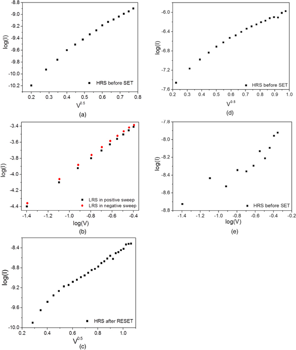
Fig. 5. (Color online) (a) Replots of I–V curves of Ag/MnOx/HfOy/Pt device with the form of log (I)−V0.5 at HRS before SET. (b) Log–log scale I–V plots of Ag/MnOx/HfOy/Pt device at LRS in positive sweep and in negative sweep. (c) Replots of I–V curves of Ag/MnOx/HfOy/Pt device with the form of log (I)–V0.5 at HRS after RESET. (d) Replots of I–V curves of Ag/MnOx/Pt device with the form of log (I)−V0.5 at HRS before SET. (e) Log–log scale I–V plots of Ag/HfOy/Pt device at HRS before SET.
Download figure:
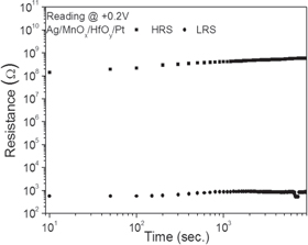
Standard image High-resolution imageFigure 6 presents the retention properties of the fabricated devices at room temperature. The resistances at HRS and LRS were measured at a reading voltage of +0.2 V with the time of up to 9000 s. The resistance ratio of HRS to LRS was well maintained in Ag/MnOx/HfOy/Pt devices. The remarkable retention ability with high resistance ratio in Ag/MnOx/HfOy/Pt devices is necessary to detect the stored information. The Ag/MnOx/HfOy/Pt devices in this study exhibited improved characteristics including low switching voltages, a high resistance ratio, and good retention properties. These confirm the potential application of the MnOx/HfOy double-layer to resistive switching memory devices.
Fig. 6. Retention properties of Ag/MnOx/HfOy/Pt devices.
Download figure:
Standard image High-resolution image
4. Conclusion
Resistive switching properties of hafnium oxide and manganese oxide double-layer films have been investigated. Compared with single layer devices, the Ag/MnOx/HfOy/Pt devices exhibited improved performances such as high resistance ratio and good retention properties. The bipolar resistive switching characteristics were attributed to the formation and disruption of Ag conductive filament in the oxide layers.
Acknowledgments
This research was supported by Myongji University's 2018 Research Fund.