

Abstract
We have demonstrated and experimentally verified the advantages of the In–Zn–O (InZnO) channel compared with the In–Ga–Zn–O (InGaZnO) channel for a high-performance oxide semiconductor channel field-effect transistor (FET) with both ultralow off-state leakage current and high on-current. Compared with the InGaZnO FET, high mobility (>30 cm2 V−1 s−1) and a reduction of source/drain (S/D) parasitic resistance by 75% were achieved by the InZnO FET. Analysis of the Schottky barrier height at the S/D contact and the band offset between the oxide semiconductor channel and gate insulator SiO2 revealed that the reduction of S/D parasitic resistance originates from the lowering of the conduction band minimum by the InZnO channel. Moreover, ultralow (<10−20 A μm−1) off-state leakage current characteristics including not only S/D leakage current but also gate leakage current were confirmed to be maintained even with a thin gate insulator with an equivalent oxide thickness of 6.2 nm.
Export citation and abstract BibTeX RIS
1. Introduction
Recently, oxide semiconductor channel field-effect transistors (FETs) in the Si complementary metal-oxide-semiconductor (CMOS) back end of line (BEOL) process have been intensively investigated.1–12) The most widely investigated oxide semiconductor material is In–Ga–Zn–O (InGaZnO). InGaZnO FETs can be fabricated by a low-temperature process as low as 400 °C in a Cu interconnection layer without thermal damage to the Si front end of line FET.3,4,11,12) Moreover, thanks to a large bandgap energy of 3.1 eV, the InGaZnO FET has unique features such as ultralow off-state leakage current characteristics (<10−22 A μm−1).8–10) By taking advantage of these features that are difficult to realize with Si MOSFETs, applications of normally-off central processing units (CPUs) and embedded memories with InGaZnO FETs in BEOL have been proposed.8–10) Thus, InGaZnO channel BEOL FETs can be expected to provide new functions as a CMOS extension.
In order to expand the applications of oxide semiconductor channel FETs to BEOL FETs, realization of both the ultralow off-state leakage current (Ioff) and high on-current (Ion) is key. However, there is an issue of low Ion in InGaZnO FETs. The mobility of a typical InGaZnO FET is around 10 cm2 V−1 s−1,1) which limits BEOL FET applications. In order to improve Ion, not only high mobility but also low source/drain (S/D) parasitic resistances are necessary, since Ion is represented as shown in Fig. 1(a) by the following equation:13)


where Vd, Rch, Rpara, μ, L, W, Cox and Vg−Vth are the channel resistance, S/D parasitic resistance, mobility, channel length, channel width, gate capacitance per unit and gate overdrive voltage, respectively. Although there are some reports on high-mobility oxide semiconductor channels such as In–Zn–O (InZnO) and In–Sn–Zn–O, parasitic resistances of those FETs have not been fully investigated.14–23) Moreover, equivalent-oxide-thickness (EOT) scaling is also effective to improve Ion. However, the impacts of the increase of gate leakage current by EOT scaling (∼nm) on ultralow Ioff characteristics are not clear.

Fig. 1. (Color online) (a) Concept of Ion improvement and (b) proposed high-performance OS Tr. with high Ion and ultralow Ioff using InZnO channel with thin EOT.
Download figure:
Standard image High-resolution imageFigure 1(b) shows our concept of the high-performance oxide semiconductor channel BEOL FET with both high Ion and ultralow Ioff. To overcome the above issues, we have demonstrated and experimentally verified the advantages of the InZnO channel compared with the InGaZnO channel in mobility and S/D parasitic resistance. In addition to the higher mobility (> 30 cm2 V−1 s−1), the InZnO FET achieved a lower parasitic resistance and a suppression of gate leakage current in the on-state. Moreover, ultralow (<10−20 A μm−1) off-state current characteristics were maintained even at a thin EOT of 6.2 nm.24) In this paper, the evaluation method of ultralow off-state leakage current characteristics is also explained in detail, and the characteristic behaviors originating from subthreshold leakage current and gate leakage current are discussed.
2. Experimental methods
Figure 2(a) shows a cross-sectional transmission electron microscope (TEM) image of the fabricated FETs. Bottom-gated and top-contact FETs were fabricated. The channel length (L) is defined as the distance between the S/D contact holes.
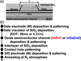
Fig. 2. (Color online) (a) Cross-sectional TEM image of fabricated oxide semiconductor and (b) fabrication process.
Download figure:
Standard image High-resolution imageFigure 2(b) shows the device fabrication process. Tungsten film was deposited on a thermally grown SiO2 layer on Si substrate using a sputtering method for the gate electrode and was patterned by photolithography. As a gate insulator, we prepared SiO2 film with an EOT of 39 nm by plasma-enhanced chemical vapor deposition (PECVD) and SiO2 film with an EOT of 6.2 nm by atomic layer deposition. Next, the oxide semiconductor channel with a thickness of 15 nm was deposited and patterned by photolithography. InZnO and InGaZnO channels were prepared for comparison. Both oxide semiconductor films were confirmed to be amorphous by TEM images. After an interlayer of SiO2 film with a thickness of 150 nm was deposited by PECVD, S/D contact holes were opened. Then tungsten film was deposited by sputtering and patterned to make S/D electrodes. The maximum process temperature during the fabrication process was lower than 400 °C.
After the fabrication, devices were annealed at 320 °C in a N2 atmosphere for 30 min and the electrical characteristics were evaluated at room temperature by a semiconductor parametric analyzer.
3. Results and discussion
3.1. Mobility improvement and S/D parasitic resistance reduction
Figure 3 shows the mobility characteristics of the fabricated InZnO FET and InGaZnO FET with an EOT of 39 nm. Each mobility was extracted by the split C−V method using FETs with an L/W of 100 μm/100 μm, where L, W is the channel length and the channel width, respectively. As shown in Fig. 3(a), the mobility of the InZnO FET was 33 cm2 V−1 s−1 at the surface carrier concentration (Ns) of 1013 cm−2, which is about twice as high as that of a typical InGaZnO FET. Figure 3(b) shows the indium (In) composition ratio dependence of the mobility of the InGaZnO FET at an Ns of 8 × 1012 cm−2. An increase of the In composition ratio is effective to improve the mobility of the InGaZnO FET.25,26) It was found that compared at the same In composition ratio of 0.56, the InZnO FET showed a higher mobility than the InGaZnO FET. This suggests that Ga acts as a carrier scattering source in InGaZnO.26,27)
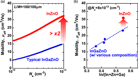
Fig. 3. (Color online) (a) Comparison of mobility characteristics between InZnO FET and InGaZnO FET and (b) In composition ratio dependence of mobility.
Download figure:
Standard image High-resolution imageNext, in order to compare S/D parasitic resistance between the InZnO FET and InGaZnO FET, we performed an Ron−L plot with FETs of different channel lengths. Figure 4(a) shows the Ron−L plot with the gate overdrive voltages from 4 V to 16 V. The value of parasitic resistance at each gate overdrive voltage was estimated from the vertical intersection point in the Ron−L plot. As shown in Fig. 4(a), the S/D parasitic resistance decreased as the gate voltage increased. This gate voltage dependence of parasitic resistance can be explained by the potential modulation of the oxide semiconductor at the S/D contact by the gate voltage due to the gate−S/D overlapped structure.28) As illustrated in Fig. 4(b), the Schottky barrier becomes narrower as the gate voltage increases, which results in the increase of tunneling in addition to thermionic field emission. Figure 5 shows a comparison of gate overdrive voltage dependence of S/D parasitic resistance between the InZnO FET and InGaZnO FET. It was found that the S/D parasitic resistance of the InZnO FET was reduced to 3.6 kΩ μm at a gate overdrive voltage of 16 V, which was about 75% smaller than that of the InGaZnO FET.
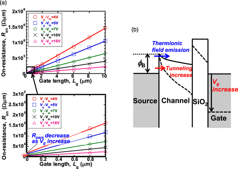
Fig. 4. (Color online) (a) Extraction method of parasitic resistance from Ron−L plot and (b) schematic illustration of gate voltage dependence of S/D parasitic resistance.
Download figure:
Standard image High-resolution image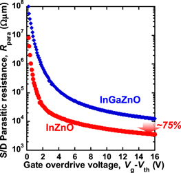
Fig. 5. (Color online) Comparison of S/D parasitic resistance between InZnO FET and InGaZnO FET.
Download figure:
Standard image High-resolution imageIn order to investigate the origin of the S/D parasitic resistance reduction by the InZnO FET, the Schottky barrier height (SBH) was extracted. Assuming that the S/D parasitic resistance at the small gate overdrive voltage is mainly dominated by thermionic field emission at the S/D contact as shown in Fig. 4(b), we fitted the S/D parasitic resistance behavior at the small gate overdrive voltage region (Vg−Vth < 1 V) with the following extended equation of the thermionic emission model:29)

where q, k, T and ϕB are the electronic charge, Boltzmann's constant, temperature and SBH, respectively. We introduced the gate bias voltage modulation factor α in this model in order to represent the gate voltage dependence of the S/D parasitic resistance by thermionic field emission and used ∼0.1 as α and 41 A cm−2 K−2 as Richardson's constant (A*).30) As shown in Fig. 6, the SBH of the InZnO FET was estimated to be 0.37 eV, while that of the InGaZnO FET was 0.46 eV. The SBH of InZnO was found to be smaller by 0.09 eV than that of InGaZnO. This indicates that the reduction of S/D parasitic resistance by the InZnO channel results from a lowering of the conduction band minimum (Ec).

Fig. 6. (Color online) Extraction of SBH from S/D parasitic resistance in small Vg−Vth region.
Download figure:
Standard image High-resolution imageSince the InZnO FET achieved a lower parasitic resistance in addition to a higher mobility than the InGaZnO FET, as shown in Fig. 3 and Fig. 5, the InZnO FET can be expected to show a higher Ion by proper channel length scaling. Figure 7 shows the Ion improvement with channel length scaling. The solid circles and squares are experimental data, and the dashed lines were calculated from each extracted mobility and parasitic resistance using Eqs. (1) and (2). The InZnO FET can be expected to have an Ion three times higher at the channel length of 10 nm than the InGaZnO FET.

Fig. 7. (Color online) Ion improvement by channel length scaling calculated from extracted mobility and S/D parasitic resistance.
Download figure:
Standard image High-resolution image3.2. Characteristics of thin EOT devices
Figure 8(a) shows a cross-sectional TEM image of the fabricated InZnO FET with thin EOT. The EOT was estimated to be 6.2 nm by C−V measurement as shown in Fig. 8(b). Figure 8(c) shows typical Id−Vg and Ig−Vg characteristics of the InZnO FET with an EOT of 6.2 nm and L/W of 1 μm/1.4 μm. The InZnO FET showed normally-off characteristics and off-state gate leakage current was not observed in the conventional DC measurement since the detection limit was about 0.1 pA.
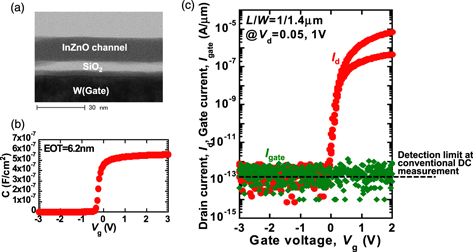
Fig. 8. (Color online) (a) Cross-sectional TEM image, (b) C−V characteristics, (c) Id−Vg and Ig−Vg characteristics of InZnO FET with EOT of 6.2 nm.
Download figure:
Standard image High-resolution imageFigure 9(a) shows a comparison of Ig−Vg characteristics in the on-state between the InZnO FET and InGaZnO FET with an L/W of 10 μm/4.4 μm. Compared with the InGaZnO FET, the Ig−Vg curve of the InZnO FET shifted positively by 0.2 V and the on-state gate leakage current was found to be suppressed by the InZnO channel. Figure 9(b) shows a Fowler−Nordheim plot of the obtained data. The on-state gate leakage current characteristics were confirmed to agree well with the Fowler−Nordheim tunneling model. This indicates that the on-state gate leakage current in the InZnO FET and InGaZnO FET with an EOT of 6.2 nm is dominated by the tunneling electron injection from the conduction band of the oxide semiconductor channel to the conduction band of the SiO2 gate insulator. The conduction band offset between the oxide semiconductor channel and the SiO2 gate insulator was estimated using the following equations of Fowler−Nordheim tunneling current (JFN):31)


where A, Eox, ϕox, m*, q and h are a constant, the oxide electric field, the band offset, the effective mass, the electronic charge and Plank's constant, respectively. Assuming that the effective mass (m*) is 0.34,32) the conduction band offsets between the oxide semiconductor channel and the SiO2 gate insulator were estimated to be 1.58 eV and 1.45 eV for the InZnO/SiO2 and InGaZnO/SiO2 interface by using the following equation, respectively. The conduction band offset of InZnO/SiO2 was found to be 0.13 eV larger than that of InGaZnO/SiO2.
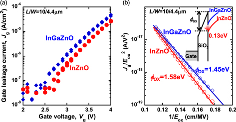
Fig. 9. (Color online) (a) Ig−Vg characteristics of InZnO FET and InGaZnO FET in on-state and (b) Fowler−Nordheim plot.
Download figure:
Standard image High-resolution imageFigure 10 shows a comparison of the extracted band diagram of InGaZnO and InZnO. Here, the bandgap energy was estimated using reflection electron energy loss spectroscopy. As shown in Fig. 5 and Fig. 9, the InZnO FET showed a reduction of S/D parasitic resistance and suppression of on-state gate leakage current. The difference of the extracted SBH values of InZnO and InGaZnO at the S/D contact was 0.1 eV, which is consistent with the difference in the extracted band offset values between the oxide semiconductor channel and SiO2 gate insulator. These results suggest that the advantages of the reduction of parasitic resistance and on-state gate leakage current in InZnO both originated from a lowering of Ec by the InZnO channel compared with the InGaZnO channel.

Fig. 10. (Color online) Schematic band diagram of InGaZnO and InZnO. The Ec of InZnO was estimated to be lower than that of InGaZnO, which may contribute to the decreases of S/D parasitic resistance and on-state gate leakage current.
Download figure:
Standard image High-resolution image3.3. Evaluation of ultralow off-state leakage current characteristics
Figure 11 shows an evaluation method of ultralow off-state leakage current characteristics.33) As shown in Fig. 11(a), we fabricated a simple circuit with the device under test (DUT), a source follower amplifier and a capacitor. The DUT and the amplifier FET of the source follower consisted of InZnO FET or InGaZnO FET, and a capacitor was monolithically fabricated on Si substrate, while an external constant current source was used as a load in the source follower amplifier. A thick SiO2 film with a thickness of 150 nm was used as an interlayer in the capacitor so that leakage current through the capacitor was negligible. Figure 11(b) shows a timing chart for evaluating the ultralow off-state leakage current characteristics. After a signal voltage (Vsig) of 1.2 V was written to the capacitor (drain of DUT), the gate voltage of DUT (Vgate) was changed to be low-level (Vg) and then Vsig was changed to be 0 V so that the potential difference between the S/D electrodes of the DUT occurred. The time dependence of the source follower amplifier's output voltage (Vdetect) was monitored and the time dependence of the floating node voltage (VFN) could be estimated by using the input−output characteristics of the source follower amplifier. Assuming that the voltage drop of the floating node is caused by leakage current via the DUT, the off-state leakage current (Ileak) can be estimated by using the following equation:

where the capacitance (CFN) of the floating node was 20 fF and each measurement time was 1000 s. This measurement was repeated with different Vg values in the off-state to obtain a gate voltage dependence of the ultralow off-state leakage current.
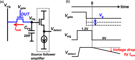
Fig. 11. (Color online) (a) Circuit diagram and (b) timing chart for evaluating ultralow off-state leakage current characteristics.
Download figure:
Standard image High-resolution imageFigure 12(a) shows the time dependences of VFN at Vg from 0 to −0.4 V. VFN at each time was calculated from the measured Vdetect by using the input−output characteristics of the source follower amplifier measured in advance. In this region, it was observed that the falling speed of VFN decreased as Vg was set more negatively, and VFN no longer decreased at Vg of −0.4 V. Moreover, as shown in the time dependences of VFN at Vg of 0 V and −0.2 V in Fig. 12(a), VFN dropped to 0 V at constant speed. This means that the magnitude of the leakage current observed in this region does not depend on the potential difference between the source and drain of the DUT. Since the subthreshold leakage current of FETs is determined by electron diffusion with thermal energy, not by the potential difference between the source and drain, the constant leakage current observed in Fig. 12(a) is consistent with the characteristics of the subthreshold leakage current. Figure 12(b) shows the transfer characteristics with the extracted leakage current values using Eq. (6). The extracted ultralow off-state leakage current values showed almost the same trend as the subthreshold characteristics obtained by conventional DC measurements. It was also confirmed that the subthreshold characteristics were maintained below 10−20 A μm−1, which is a detection limit of this method.

Fig. 12. (Color online) (a) Time dependence of VFN at the gate voltage from 0 V to −0.4 V and (b) transfer characteristics with extracted leakage current values.
Download figure:
Standard image High-resolution imageFigure 13(a) shows the time dependences of VFN at Vg less than −2 V. In this region, as Vg decreases negatively, VFN drops dramatically. Unlike the constant leakage current observed in Fig. 12(a), the leakage current showed time dependence and the time derivatives were decreased as the drain voltage of the DUT was reduced due to the leakage current from the floating node. This behavior of VFN dropping is consistent with the characteristics of gate leakage current between the drain and gate of the DUT. Figure 13(b) shows the transfer characteristics with the extracted leakage current values. Since the gate leakage current was reduced as the drain voltage of the DUT was decreased, the initial time derivative of VFN was used to estimate a leakage current value at each gate voltage. It was confirmed that gate leakage current over 10−20 A μm−1 was not observed in the range of ∣Vg∣ < 1.5 V even at a thin EOT of 6.2 nm.
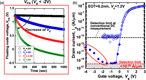
Fig. 13. (Color online) (a) Time dependence of VFN at a gate voltage less than −2 V and (b) transfer characteristics with extracted leakage current values.
Download figure:
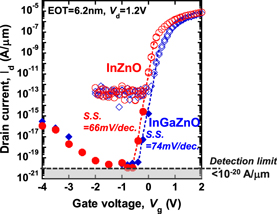
Standard image High-resolution imageFinally we compared ultralow off-state leakage current characteristics between InZnO FET and InGaZnO FET extracted from the above evaluation method (Fig. 14). Ultralow off-state leakage current values of the InZnO FET and InGaZnO FET agreed well with the trends of the subthreshold characteristics of the InZnO FET and InGaZnO FET by conventional DC measurements, respectively. The subthreshold slope (S.S.) values maintained below 10−20 A μm−1 were 66 mV dec−1 and 74 mV dec−1 for the InZnO FET and InGaZnO FET, respectively. It was found that off-state gate leakage current characteristics were comparable between the InZnO and InGaZnO FET. The InZnO FET with an EOT of 6.2 nm exhibited ultralow off-state leakage current characteristics (<10−20 A μm−1) as well as the InGaZnO FET in the range of ∣Vg∣ < 1.5 V.
Fig. 14. (Color online) Comparison of ultralow off-state leakage current characteristics between the InZnO FET and InGaZnO FET with an EOT of 6.2 nm.
Download figure:
Standard image High-resolution image
4. Conclusions
We have demonstrated and verified the advantages of the InZnO channel compared to InGaZnO. The InZnO FET achieved a mobility as high as 33 cm2 V−1 s−1 along with a drastic decrease of parasitic resistance up to 75% compared with the InGaZnO FET. Comprehensive investigation of the SBH at the S/D contact and the band offset at the oxide semiconductor/SiO2 revealed that the parasitic resistance reduction by the InZnO channel originates from a lowering of Ec. Ultralow off-state leakage current characteristics (<10−20 A μm−1) can be maintained even at a thin EOT of 6.2 nm. Thus the InZnO FET is highly promising as a high-performance oxide semiconductor BEOL transistor with both ultralow Ioff and high Ion.