

Abstract
Although ferroelectric random access memory (FRAM) has superior electric properties, its downside is that it has a relatively larger cell area in comparison other non-volatile memories. We tried to apply TiOx, and AlOx to an underlying layer (TiOx-UL, AlOx-UL) instead of our previously used Ti underlying layer (Ti-UL) for the La-doped lead zirconate titanate (PLZT) capacitor to obtain a high polarization value aiming to a lowering cell area. The failed bit ratio of the FRAM with TiOx-UL was found to be higher than that with AlOx-UL even though polarization values of the PLZT capacitor with both underlying layers are almost the same and much higher than that with Ti-UL. It is strongly suggested that the imprint induced in PLZT by charged defect is a main cause of bit failure by fail-bit analysis. X-ray diffraction and atomic force microscopy observations shows that charged defect density in PLZT over TiOx-UL is possibly higher than that in PLZT over AlOx-UL due to surface roughness of underlying layers.
1. Introduction
Internet of Things (IoT) have gained ground on our life for years. From smart devices for private use including smart phones and smart watches to edge devices for business use such as routers, integrated access devices (IADs), and multiplexers,1) various kinds of devices have connected to the Internet. In those devices, non-volatile memory (NVM) plays an important role not only to hold memories even without outer electric power but also to hold system security and authentication.2) Some devices, such as wearable devices, power meters and drive recorders, need high writing speed, high rewriting endurance and low power consumption. Although FLASH memory is a typical NVM widely used in various devices, it is not suitable for the above-mentioned devices because of its long-time rewriting as well as a small rewriting limit of about 105.3, 4) There have been attempts to apply some emerging NVMs to devices using IoT by taking advantage of their low stand-by current and high memory density,4) this includes: spin-torque transfer magnetoresistive memory (STT-MRAM), this has been reportedly promising due to its high writing speed, good rewriting endurance and high memory density. However, it has not yet been able to decrease the probability of disturbance error during reading and lower power consumption during accessing.5) Phase change random access memory (PRAM) is also a promising NVM with high memory density with a cross-bar structure. It has a drawback of high current density during switching "set" and "reset" states resulting in high energy consumption.6) Resistive random access memory (ReRAM) is another emerging NVM with high memory density and low energy consumption. However, it has struggled with its large sneak current and low rewriting endurance.7)
Since ferroelectric random access memory (FRAM) is the first commercialized emerging NVM, it has been studied for a long time8–10) and has been proven to have superior properties corresponding to the above-mentioned demands for devices using in IoT.2,11) We have mass-produced FRAM since 1999 and improved its performance including the device reliability though our over 19-year production experiences.11,12) However, it has relatively larger cell area or unit memory area than other conventional and emerging NVNs mainly due to large ferroelectric capacitor footprint. We tried to reduce the FRAM-cell area by optimizing materials used in ferroelectric capacitors.13,14) The bottom electrode (BE) of the ferroelectric capacitor plays an important role to determine the crystalline quality and electric properties of ferroelectrics, especially for the ferroelectrics deposited by sputter-deposition and solid-solution deposition (SSD) methods, which need post deposition annealing (PDA).15–24) Because PDA for crystallizing oxide ferroelectrics is generally carried out at high temperatures, generally over 600 °C, in oxygen (O2) atmosphere, noble metals, such as Pt ant Ir, are employed as a BE. For example, Pt is typically used as a BE for lead zirconate titanate (PZT) and its related ferroelectrics with an Ti-adhesion layer (Pt/Ti BE).15–18) It was reported that Pt/Ti BE had some problems such as hillocks appearing on the Pt surface and a cause of low rewriting endurance (fatigue).18) Although, many types of conductive oxides as an alternative BE material have been proposed, these materials are not easily handled in FRAM fabrication process because of the difficulty in keeping the stoichiometry of their composed elements. On the other hand, it has also been reported that some oxide materials, such as TiO2,19,20) Al2O3,21) RuO2,22,23) and LaNiO3,24) as an underlying layer of Pt-BE led to good electric properties of PZT capacitors. Although these underlying materials were studied in the early stages of FRAM development from 1990s to early 2000s, those were mainly developed to focus only on the crystalline quality of the ferroelectrics and its electric properties. However, material choice of the underlying layer of the Pt BE is presently an important issue to determine FRAM mass producibility, especially its production yield. Although we try to reduce the footprint of the ferroelectric capacitor by employing a TiOx underlying layer (TiOx-UL) of Pt BE instead of our previously used Ti underlying layer (Ti-UL)12) because we found that polarization of the La-doped lead zirconate titanate (PLZT) capacitor with TiOx-UL was larger than that of Ti-UL in our experiments. The number of the failed bit in FRAM comprising the PLZT capacitor with TiOx-UL was found to be larger than that of FRAM with ferroelectric capacitor using Ti-UL. In our FRAM production using conventional silicon (Si) mass production, it is important to choose materials for the ferroelectric capacitor that includes BE without cross-contamination and being easily patterned or etched by conventional equipment. Upon further investigation, we found that the AlOx underlying layer (AlOx-UL) could achieve both high polarization and a good FRAM production yield. In this paper, we describe the relationship among the crystalline quality of ferroelectric material, its electric property, and FRAM production yield using Ti-UL, TiOx-UL, and AlOx-UL for Pt BE, and discuss about the reason why the PLZT capacitor with an AlOx-UL revealed good electric performance and production yield.
2. Experimental methods
In our FRAM fabrication process, the ferroelectric capacitor fabrication process is inserted between transistor fabrication on a Si substrate and metallization. In the ferroelectric capacitor fabrication process in this experiment, we prepared 20-nm thick Ti-UL, or AlOx-UL by sputtering on a SiO2-coated Si substrate in which transistors were fabricated in advance. A Ti-UL was oxidized by rapid thermal annealing (RTA) at 700 °C in 1%-O2 mixed Ar atmosphere to obtain a TiOx-UL with a thickness of about 30 nm. Table I shows the fabrication conditions of each underlying layer. After depositing a 150 nm-thick {111}-oriented Pt BE on the underlying layer at 350 °C and annealing it at 650 °C in Ar atmosphere, we deposited a 150 nm thick PLZT layer by radio-frequency (RF) sputtering under 1.0-Pa Ar-pressure at room temperature. Atomic concentration of La and the Zr/Ti ratio are 2.0 mol% and 0.4/0.6, respectively. Specimens were annealed (PDA) at 600 °C in 1.25%-O2 mixed Ar by RTA following by deposition of a 200-nm thick IrOx layer as a top electrode (TE) on the PLZT by reactive sputtering in the Ar + O2 atmosphere using an Ir target. Crystalline qualities of the Pt BE and PLZT were characterized by X-ray diffraction (XRD) using Huber goniometer equipped with a two-dimensional pixel detector PILATUS-100 K (DECTRIS) at undulator beamline BL16XU of SPring-8. We measured the polarization properties using a Sawyer-Tower circuit consisting of a pulse generator (Keysight 81110A or 33250A) and a digitizing oscilloscope (Keysight 54845A). Since the conventional polarization versus electric field (P-E) hysteresis loop does not necessarily reflect the real operation of the FRAM device, switching charge is measured using a 4-pulse sequence (PUND) approach that mimics the actual FRAM operation.25–27) We explored the atomic inter-diffusion from the PLZT to the underlying layer through the Pt BE and vice versa using secondary ion mass spectroscopy (SIMS). The SIMS measurements were performed by CAMECA 4550. We selected mass filtered Cs+ ions at an energy of 5 keV as the primary beam and monitored Pb+, Pt+, Ir+ and CsM+ (M = O, Si, Ti and Al) secondary ions. Impacted angle of the Cs+ ion was 45° with the normal to the sample surface. Surface roughness of the underlying layers was measured by a Nanoscope III Dimension 5000 (Digital Instruments) atomic force microscopy (AFM) with a standard Si tip in the tapping mode. After FRAM fabrication, we finally evaluated the production yield by probing 256-Kb FRAM test circuits after baking them over 150 °C.
Table I. Underlying layers we tried in this experiment with their deposition and annealing (only TiOx-UL) conditions.
| Sample name | Ti-UL | TiOx-UL | AlOx-UL |
|---|---|---|---|
| Material | Ti | TiOx | AlOx |
| Target material | Ti | Ti | AlOx |
| Sputtering Current | DC | DC | AC |
| Sputtering Gas | Ar | Ar | Ar |
| Sputtering Pressure (Pa) | 0.2–0.4 | 0.2–0.4 | 0.8–1.2 |
| Deposition Temperature (°C) | 150 | 150 | 20 |
| Sputtering Power (W cm−2) | 3.68 | 3.68 | 2.83 |
| Sputtering Time (s) | 11 | 11 | 40 |
| RTA Gas | — | Ar/O2 | — |
| RTA Temperature (°C) | — | 700 | — |
| Thickness (nm) | 20 | ∼30 | 20 |
3. Results and discussion
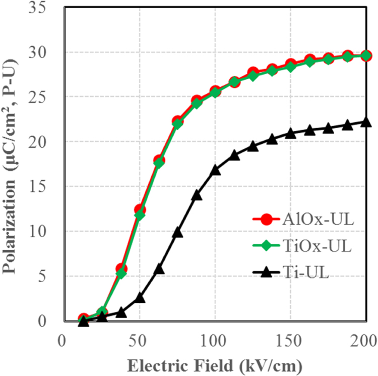
We investigate the relationship between the applied electric field and polarization of the PLZT capacitors with Ti-UL, TiOx-UL, or AlOx-UL as shown in Fig. 1, where polarization means the values obtained by subtracting the U-term value from P-term values. It is clear that polarization values of the capacitors with TiOx-UL and AlOx-UL are almost the same at every applied field, whereas the polarization values of the capacitor with Ti-UL are much lower than those with the other two underlying layers. We also investigated inter-diffusion of PLZT and SiO2 interlayers across the Pt BE by SIMS, as show in Fig. 2. It is observed that much larger amount of Pb diffused across the Pt BE/Ti than those across the Pt BE/TiOx and Pt BE/AlOx. S-H. Kim et al.21) reported that Al2O3 underlying layer, as a diffusion barrier between the silicon substrate and the Pt BE, suppressed interface reactions between the film and the substrate, and prevented the inter-diffusion of Pb and Si elements resulting in good electric properties of the PZT capacitor. Although, the authors employed sol-gel derived PZT for the ferroelectric capacitor in their study, our PLZT growth processes is similar to their growth process that PZT in amorphous phase was crystallized on the Pt BE by PDA. PbO inter-diffusion possibly occurred in the PLZT capacitor with Ti-UL because of large Pb and O signal intensities of SIMS in the Pt BE region,28) as shown in Figs. 2(a) and 2(b). However, Fig. 2(c) shows that Si diffusion is larger in the PLZT capacitors with AlOx-UL and Ti-UL than that in the PLZT capacitor with TiOx-UL, which is slightly different from their conclusions. In our experiments, Si inter-diffusion does not appear to affect the polarization-voltage behavior, as shown in Fig. 1. It is possible that the quality of their Al2O3, which was obtained by sol-gel coating and 750 °C PDA, is different from our AlOx-UL. Therefore, higher polarization obtained by PLZT capacitor with TiOx-UL and AlOx-UL than that with Ti-UL should be owing to prevention of Pb inter-diffusion across Pt BE by TiOx-UL and AlOx-UL. It should be noted that slight shift of O and Si profiles for the specimen with TiOx-UL to the right side, as shown in Figs. 1(b) and 1(c), should be due to TiOx-UL being thicker than Ti-UL and AlOx-UL.

Fig. 1. (Color online) Electric field dependence of the polarization defined by the difference between P term and U term21–23) for the ferroelectric capacitors with the Ti-UL, TiOx-UL, and AlOx-UL.
Download figure:
Standard image High-resolution image
Fig. 2. (Color online) Depth profiles of (a) Pb, (b) Si, and (c) O of ferroelectric capacitor with the Ti-UL, TiOx-UL, and AlOx-UL measure by SIMS.
Download figure:
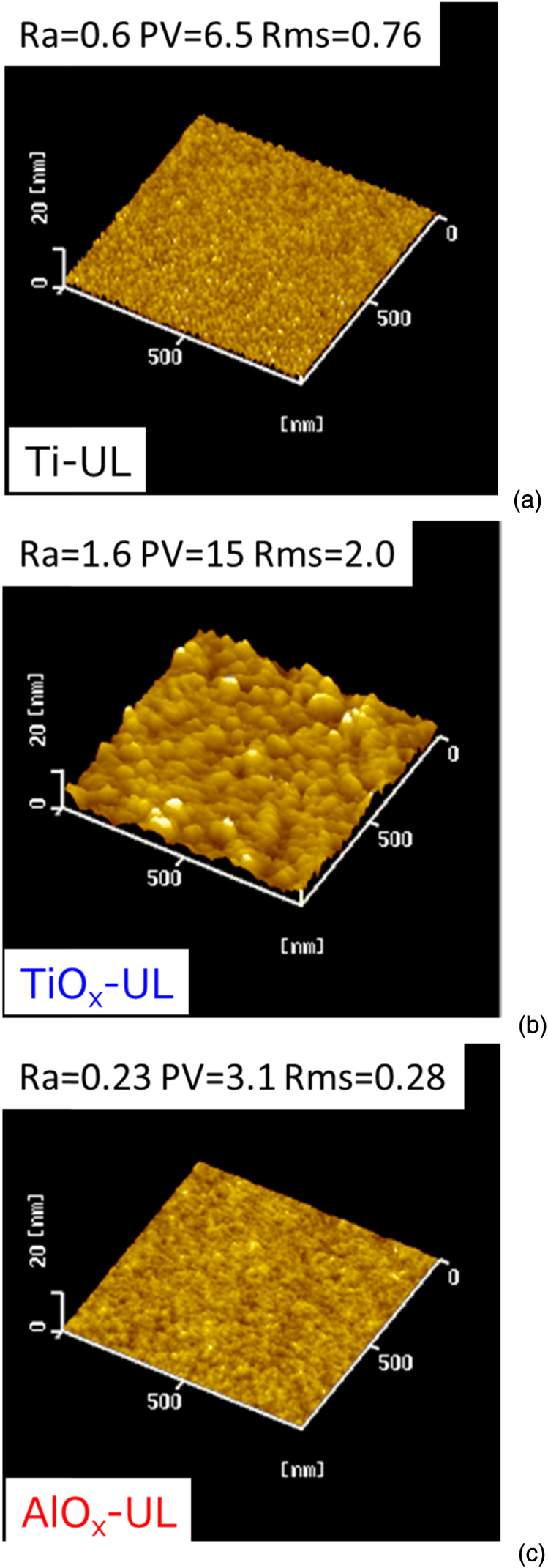
Standard image High-resolution imageOn the other hand, the number of failed bit of FRAM comprising the PLZT capacitor with TiOx-UL is much higher than those of FRAM with Ti-UL and AlOx-UL as shown in Fig. 3. Thus, we tried to investigate the surface morphology and crystalline quality of each underlying layer by AFM and XRD, respectively. Figure 4 shows the surface images of three underlying layers obtained by scanning an area of 1-μm2 where Ra, Rms, and PV indicate calculated average roughness, root mean square roughness, and peak-to-valley roughness, respectively. Those AFM images reveal that TiOx-UL has a rougher surface than Ti-UL and AlOx-UL. XRD measurements of TiOx-UL and AlOx-UL shows that TiOx-UL are crystallized after PDA whereas AlOx is not crystallized enough or in amorphous phase, as shown in Fig. 5. Those crystalline states (well crystalized or amorphous) supposedly influence in the surface roughness of AlOx-UL and TiOx-UL. We also evaluated full-width at half maximum (FWHM) of the {111}-Pt and {111}-PLZT XRD peaks, as shown in Fig. 6, by rocking-curve measurement to investigate the crystalline orientation of the Pt and PLZT layers. Unstable behavior of the XRD curve obtained by the PLZT layer over TiOx-UL is due to a low signal-noise ratio. It is clear that FWHM both of the {111}-Pt and {111}-PLZT XRD peaks from the PLZT and Pt layers over the TiOx-UL are much larger than those from the PZT and Pt layers over both Ti-UL and AlOx-UL. FWHM of the {111}-Pt and {111}-PLZT peaks from the PLZT on Ti-UL slightly larger than those from the PLZT on AlOx-UL. Those results indicate that the Pt and PLZT layers on AlOx-UL has higher {111}-crystalline orientation than the Pt and PLZT layers over both TiOx-UL and Ti-UL. Surface roughness of underlying layers apparently influences in the crystalline quality of the Pt and PLZT layers as shown in Fig. 7 and furthermore, the number of failed bit in FRAM nonlinearly increases with the increase in surface roughness of the underlying layer, as shown in Fig. 8. In reality, the FRAM comprising the PLZT capacitor with AlOx-UL significantly decreases the failed bit ratio by 63% in comparison with the previous FRAM comprising the PLZT capacitor with TiOx-UL as shown in Fig. 3. We infer that PLZT with lower crystalline orientation of PLZT should have more crystalline defects near the grain boundary than the PLZT with higher orientation. These defects were possibly charged29) causing fatigue and imprint28,30–34) of the PLZT capacitor, eventually resulting in lowering FRAM production yield, even though the PLZT capacitor has enough polarization values as in the case of TiO2-UL. Thus, we directly measured polarization-voltage (P-V) hysteresis of the PLZT capacitor with TiOx-UL for several failed and normal bits by AFM. Figure 9 shows typical P-V hysteresis curves of a failed and a normal bit. P-V hysteresis of all failed bits are found to shift toward to the positive-voltage direction, whereas P-V hysteresis of the normal bits keeps in normal position, which indicates that imprint induced by charged defects in the PLZT over TiOx-UL is a main cause of a bit failure of FRAM. It is strongly suggested that high density of charged defects induced in PLZT of capacitor with TiOx-UL should lower the FRAM production yield. Finally, it should be noted for the case of Ti-UL, alloyed Pt and Ti by PDA possibly does not largely affect the crystalline orientation of Pt and PLZT eventually resulting in relatively high FRAM production yield.

Fig. 3. (Color online) Number of fail bits for the 256 Kb FRAM comprising PLZT capacitors with Ti-UL (black), TIOx-UL (green), and AlOx-UL (red).
Download figure:
Standard image High-resolution image
Fig. 4. (Color online) Surface images of the (a) Ti-UL, (b) TiOx-UL, and (c) AlOx-UL, obtained by AFM. Ra, Rms, and PV indicate calculated average roughness, root mean square roughness, and peak-to-valley roughness, respectively.
Download figure:
Standard image High-resolution image
Fig. 5. (Color online) XRD patterns of (a) TiOx-UL and (b) AlOx-UL obtained by 2θ-θ measurement.
Download figure:
Standard image High-resolution image
Fig. 6. (Color online) (a) {111}-Pt and (b) {111}-PLZT XRD patterns obtained by rocking curve measurement.
Download figure:
Standard image High-resolution image
Fig. 7. (Color online) Relationship between (a) FWHM of {111}-Pt XRD peak and surface roughness (root mean square) of underlying layer, and (b) FWHM of {111}-PLZT XRD peak and surface roughness (root mean square) of underlying layer.
Download figure:
Standard image High-resolution image
Fig. 8 (Color online) Relationship between number of fail-bit for 256-Kb FRAM test chip and surface roughness (root mean square) of underlying layer.
Download figure:
Standard image High-resolution image
Fig. 9 (Color online) Polarization-voltage hysteresis curves of the PLZT capacitor with TiOx-UL for a failed (red circle) and a normal bit (green cross) measured by AFM.
Download figure:
Standard image High-resolution image
4. Conclusions
We tried to apply TiOx and AlOx underlying layers (TiOx-UL, AlOx-UL) of the Pt bottom electrode (BE) for La-doped Pb(Ar, Ti)O3 (PLZT) capacitor comprised in ferroelectric random access memory (FRAM) instead of our previously used Ti underlying layer (Ti-UL), aiming to enlarge memory density by increasing the polarization value of the PLZT capacitor. We have succeeded to obtain higher polarization values of PLZT capacitor with TiOx-UL and AlOx-UL than that with Ti-UL, owing to the prevention of Pb inter-diffusion across the Pt BE by TiOx-UL and AlOx-UL. However, the production yield of the FRAM with TiOx-UL is found to be lower than that of AlOx-UL. X-ray diffraction (XRD) measurement shows that crystalline orientation of the PLZT and Pt layers on AlOx-UL is higher than those on TiOx-UL, and also that AlOx-UL is amorphous whereas TiOx is crystallized. Atomic force microscopy (AFM) reveals that the surface roughness of TiOx is higher that of the AlOx underlying layer which possibly affects the crystalline orientation of Pt and PLZT layers. We infer that charged defect density of the high crystalline quality PLZT should be lower than that of low crystalline quality PLZT. Charged defects in ferroelectric material are known to degrade the ferroelectric capacitor as phenomena of fatigue and imprint. We found imprinted polarization-voltage hysteresis of a PLZT capacitor with a TiOx underlying layer of failed bit in FRAM by direct AFM measurement. Thus, it is strongly suggested that imprint in PLZT induced by charged defect is a main cause of bit failure in FRAM. Because PLZT on Pt BE with TiOx-UL probably has a higher charged defect density than PLZT with AlOx-UL, production yield of FRAM with AlOx-UL is possibly higher than that of FRAM with TiOx-UL. Therefore, we conclude AlOx is more suitable for the underlying layer of Pt BE than TiOx-UL.