
Abstract
We report on an approach to produce single photon emitters at the SiO2/SiC interface. We form a high-quality SiO2/SiC interface by high-temperature oxidation and subsequently perform oxidation at lower temperatures (200 °C–1000 °C) to generate the emitters. After reoxidation at 800 °C, we confirmed the formation of emitters with a bright luminescence (>50 kcps). Through Hambury-Brown and Twiss measurements, single photon characteristics were confirmed. Thus, the proposed approach is effective in generating highly bright single photon emitters at the SiO2/SiC interface.

Content from this work may be used under the terms of the Creative Commons Attribution 4.0 license. Any further distribution of this work must maintain attribution to the author(s) and the title of the work, journal citation and DOI.
Single photon emitters (SPEs) that can emit non-classical light at arbitrary timing are fundamental elements in future quantum applications including communication 1) and computing. 2) In particular, point defects in wide bandgap semiconductors may serve as SPEs; single photons could be emitted through the transition between the defect levels. In this context, the best-studied defect is the negatively charged nitrogen-vacancy (NV) center in diamond. Quantum interference between indistinguishable photons from remote NV centers has been demonstrated. 3)
Silicon carbide (SiC) is a wide bandgap material attractive for quantum applications. Its well-established crystal growth, conductivity control, and process technologies make this material appealing as a host for quantum defects. At present, point defects in SiC such as silicon vacancy (VSi), 4–7) divacancy (VC VSi) 8,9) and nitrogen-vacancy (NC VSi) 10–12) defects were reported to act as SPEs with defect spins. Previous experimental studies also pointed out emitters without optically detected magnetic resonance including the carbon antisite-vacancy (CSi VC), 13) TS, 14) and DI 15) centers. The interface of silicon dioxide (SiO2) and SiC is also of interest. A high density of defects is present at the SiO2/SiC interface, which is the major cause of mobility degradation in SiC MOSFETs. 16) The plausible origin of the defects is carbon-related complexes 17–20) generated during the thermal oxidation process of SiC. A part of these interface defects is known to behave as an SPE with bright emissions. 21–25) Furthermore, interface defects can be readily implemented in electrical devices, enabling control over their luminescence via electrical current/voltage. 21,23,26) However, emitter density control at the SiO2/SiC interface is not straightforward. For a SiO2/SiC interface formed by oxidation at a typical temperature (1200 °C), the defects are not necessarily isolated. In such a case, individual defects may not serve as SPEs due to luminescence overlap. 27,28) To develop quantum applications, it is crucial to have control over the density of defects. So far, density control has been achieved by changing the conditions of oxidation and annealing. For example, post-oxidation annealing in nitric oxide (NO) 29,30) is effective in reducing the density of luminescent defects. 24) More recent studies have achieved density control of defects and the formation of SPEs via post-oxidation annealing in carbon dioxide (CO2) 27) or oxidation followed by cooling in nitrogen (N2) ambient. 28)
Most of the aforementioned studies focused on the reduction in defects via the optimization of the oxide formation process. In this study, we report on an alternative approach; we first prepare a SiO2/SiC interface with low defect density and produce the defects in the following processing steps. Specifically, we form a high-quality SiO2/SiC interface by high-temperature oxidation (HTO) at 1600 °C 31) and subsequently perform oxidation at temperatures below 1000 °C. Unlike the previous study where oxidation of a SiC surface was examined in detail, 22) we investigated defect formation at a SiO2/SiC interface. This enables us to evaluate the interface defects both electrically and optically and to discuss their correlation. Our aim is to control the defect density over a wide range and establish a process to form SPEs.
Figure 1(a) shows the flow of sample preparation and measurements. We used 4H-SiC(0001) samples with 5 μm thick n-type epilayers (donor density: 1.0 × 1016 cm−3). The samples were cleaned with acetone, piranha, SC1, SC2, and 10% hydrofluoric acid and then rinsed with ultrapure water. After that, a SiO2 layer was formed by HTO at 1600 °C for 4.5 min in low oxygen partial pressure conditions [0.3% O2/argon(Ar)]. 31) After cooling the samples to room temperature, reoxidation was performed at lower temperatures ranging from 200 to 1000 °C for 10 min in 100% O2. The resulting SiO2 thickness was about 30–40 nm. The samples were labeled on the basis of the oxidation conditions, e.g. "HTO", "HTO + Ox. 200 °C", and "HTO + Ox. 400 °C". An as-cleaned sample without oxidation was also prepared for comparison: sample "SiC w/o Oxide". Figure 1(b) describes the concept of sample preparation. We first form a high-quality SiO2/SiC interface by HTO and then generate SPEs at the interface by subsequent low-temperature reoxidation. Optical measurements were performed on these SiO2/SiC samples. In the measurements, a green laser (wavelength: 532 nm) was used for defect excitation. Then, luminescence above 550 or 600 nm was collected through an objective lens (NA = 0.9) and detected either by a spectrometer or single photon counting modules based on a silicon avalanche photodiode. Specific optical setups are described in Ref. 27. In the present study, confocal photoluminescence (PL) mapping, PL spectroscopy, and Hanbury-Brown and Twiss (HBT) measurements 32,33) were carried out. Excitation laser power was set to 0.5 mW for all the optical measurements. The instruments for optical measurements are controlled using MAHOS software. 34) For electrical measurements, aluminum (Al) gate electrodes (diameter: 100 μm) and back contacts were formed by vacuum evaporation to fabricate MOS capacitors. Then, capacitance–voltage (C–V) measurements were performed to evaluate the interface properties. All measurements were carried out at room temperature.

Fig. 1. (a) Flow of sample preparation and measurements. (b) Schematic illustration describing the concept of sample preparation in this study.
Download figure:
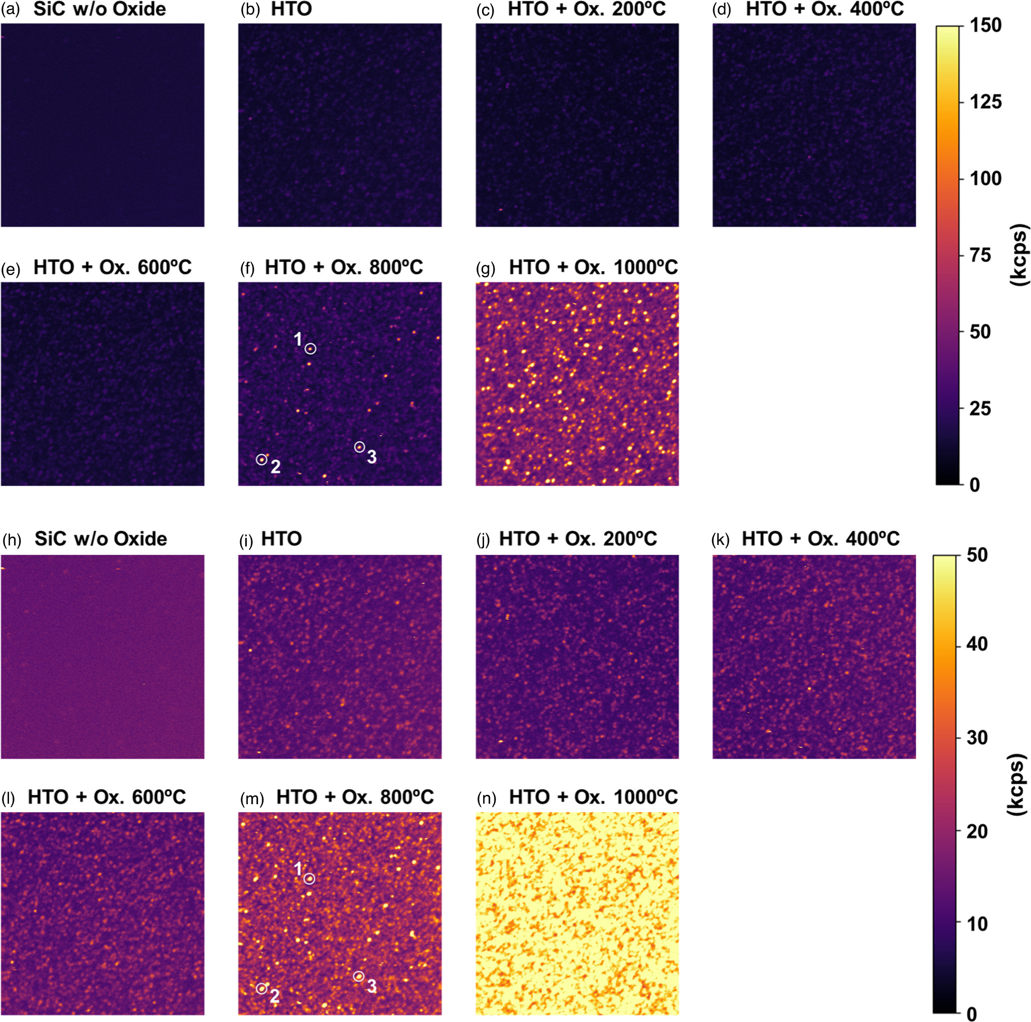
Standard image High-resolution imageFigure 2 shows the confocal PL mapping images taken from SiC and SiO2/SiC samples; different scale bars are applied for Figs. 2(a)–2(g) and 2(g)–2(n). The scan area was 30 × 30 μm2. First, the sample formed by HTO exhibited negligible bright spots in the image [Fig. 2(b)]; the density of color centers which exhibited count rates above 50 kcps was 4.4 × 105 cm−2 (lower detection limit: 1.1 × 105 cm−2), sufficiently low compared to a sample formed by 1200 °C oxidation (5.2 × 107 cm−2) measured with the same optical setup. 27) When looking closely at the interface [Fig. 2(i)], the generation of dim spots can be confirmed after HTO. However, their luminescence is rather weak and the averaged intensity within the scanning area is ∼14 kcps, comparable to that of the sample without oxidation (∼15 kcps). Therefore, HTO is effective in suppressing the defects with bright luminescence as well as electrical defects. 31) From this starting point, we perform additional oxidation at lower temperatures to generate the defects. We can see that the high-quality interface with less luminescent defects is maintained up to an oxidation temperature of 600 °C. This suggests that oxidation does not proceed in this temperature regime. Note that the situation differs from Ref. 22, where the oxidation of SiC starts to proceed at 550 °C. While oxidation of a bare SiC surface is investigated in Ref. 22, the SiC surface is covered by a SiO2 layer (30–40 nm) formed by HTO in our case. This likely results in the difference in the boundary temperature at which the oxidation proceeds. After oxidation at 800 °C, distinguishable spots with bright luminescence (>50 kcps) were clearly confirmed [Fig. 2(f)]. The areal density of these bright spots was estimated as 8.1 × 106 cm−2 through image processing. When the temperature was further increased to 1000 °C, the bright luminescent spots covered the entire surface of the sample [Figs. 2(g) and 2(n)]. By manually counting the spots, the color center density was determined as 4.6 × 107 cm−2. To summarize, we demonstrated the density control of the color centers with bright luminescence (>50 kcps) within a range of 105–107 cm−2.

Fig. 2. Confocal photoluminescence mapping images of SiC and SiO2/SiC structures. Different scale bars are applied for (a)–(g) and (h)–(n). The mapping area was 30 × 30 μm2.
Download figure:
Standard image High-resolution imageFigure 3(a) is a close-up PL mapping image for three typical spots for the 800 °C-reoxidized sample. The labeled numbers correspond to those in Fig. 2(f) and 2(m). We found that bright spots were formed after oxidation at 800 °C. We then evaluated the second-order correlation function, g2(τ) through HBT measurements to investigate the single photon characteristics of the defects. Figure 3(b) shows the g2(τ) as a function of delay time for the three spots shown in Fig. 3(a). As shown in these typical examples, the g2(0) values were below 0.5, indicating that all the spots serve as SPEs. We investigated 20 stable bright spots in total with all serving as SPEs. Therefore, the approach to form a high-quality interface as the first step and to generate the defects by reoxidation is effective in forming SPEs. In contrast, we note that only 4 out of 6 spots showed g2(0) below 0.5 after oxidation at 1000 °C. This clearly indicates the importance of forming separated emitters; when the luminescence from several emitters overlaps within the resolution of the setup, individual defects no longer serve as SPEs. Note that our claim is not that 800 °C is the optimum temperature to generate the emitters. Although the g2(0) values were below 0.5 for the investigated spots, one may notice that the optimum oxidation temperature lies between 600 °C–800 °C to make the emitters spatially well isolated. The significance is rather the strategy to form a high-quality interface as the first step and to generate the emitters in the following processing steps. Figure 3(c) shows the PL spectra for the three spots in Fig. 3(a). Despite the high emission rate from the spots (>50 kcps), broad PL spectra varying from one another were observed as in previous reports. 21,22,27,28)

Fig. 3. (a) PL mapping image (mapping area: 3 × 3 μm2), (b) results of HBT measurements, and (c) PL spectra for three typical color centers in the sample HTO + Ox. 800 °C. In (b), blue dashed lines indicate g2(τ) = 0.5. In (c), note that the two sharp peaks located above 2.2 eV are the transverse and longitudinal optical Raman signals of 4H-SiC crystal, respectively. 21,38,39)
Download figure:
Standard image High-resolution imageWe then evaluated the C–V characteristics of SiC MOS capacitors to investigate the electrical properties. Figure 4 shows the normalized C–V curves of SiC MOS capacitors formed by HTO and additional oxidation at 200 °C–1000 °C. The C–V measurements were conducted by sweeping the gate voltage from depletion (−10 V) to accumulation (+12 V) at a measurement frequency of 1 MHz. First, steep C–V characteristics were obtained for the sample formed by HTO. This indicates low interface defect density, in accordance with Ref. 31. We then look into the effects of additional oxidation. When the oxidation temperature was below 600 °C, little change in the characteristics was observed. This means that the high-quality interface formed by HTO is maintained up to an oxidation temperature of 600 °C. This coincides with the observation of optical measurements (Fig. 2) where the luminescent spots were hardly generated by oxidation in this temperature regime. In contrast, after oxidation at or above 800 °C, a significant positive shift in the C–V characteristics was observed. This clearly indicates the increase in the electrically active defects. With the further increase in the oxidation temperature to 1000 °C, the defect formation was even pronounced and the interface properties were severely deteriorated.

Fig. 4. Normalized C–V characteristics of SiC MOS capacitors: samples HTO and HTO + Ox. 200 °C–1000 °C (measurement frequency: 1 MHz).
Download figure:
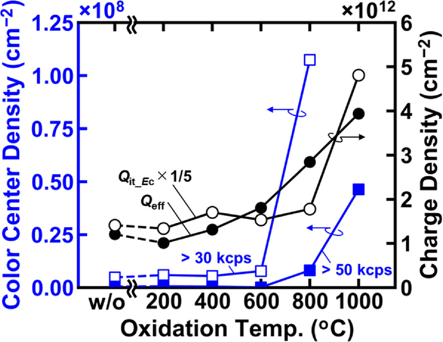
Standard image High-resolution imageTo show the correlation between the optically and electrically active defects more clearly, we plotted both the color center density and interface charge density as a function of process condition. Figure 5 shows the color center density with count rates greater than 30 or 50 kcps, the effective fixed charge density (Qeff) at the interface, and the interface defect density near the conduction band edge (Qit_Ec) as a function of reoxidation temperature. For samples reoxidized at temperatures below 800 °C, the color centers were counted through image processing. For the sample oxidized at 1000 °C, the color centers were manually counted. Qeff was estimated from the shift in the flatband voltage (ΔVFB) from its ideal position using the following formula:

where COX is the oxide capacitance per unit area calculated from the measured accumulation capacitance and e is the elementary charge. VFB was determined as the gate voltage where the capacitance equals the theoretical flatband capacitance (CFB). In the case of SiC MOS structures with relatively high defect density, Qeff generally represents the total amount of acceptor-type interface defects including the contribution of deep traps. Qit_Ec was estimated by integrating the interface state density near the conduction band edge (i.e. Ec–E = 0.2–0.6 eV) obtained by a high(1 MHz)-low method. As a result, a certain correlation was found between the color center density and the Qeff; a rapid increase was observed at reoxidation temperatures above 800 °C. In contrast, the Qit_Ec significantly increased at 1000 °C. This suggests that the color centers generated at the SiO2/SiC interface by the reoxidation originate from deep electron traps rather than shallow ones.
Fig. 5. Color center density and charge density at a SiO2/SiC interface as a function of reoxidation temperature. "w/o" corresponds to the sample HTO.
Download figure:
Standard image High-resolution image
Here we discuss the possible origin of emitters created during the oxidation process of SiC. First, we found that HTO is effective in reducing the density of emitters [Fig. 2(b)]. As stated in the introduction, carbon-related defects are regarded as the most prominent candidate for defects found at the SiO2/SiC interface. On the basis of energetics or thermodynamic considerations, oxidation at high temperatures seems effective in reducing the carbon-related defects at/near the interface. 20,31,35) Incidentally, a study based on electrically-detected magnetic resonance (EDMR) spectroscopy showed that HTO suppresses the signal originating from the carbon dangling-bond defect (PbC center) at the SiO2/SiC interface. 36) In contrast, a high density of carbon-related defects should be formed at the interface when oxidation is performed at moderate temperatures (about 800 °C–1000 °C). Since the emitters were generated during the reoxidation process in this study, carbon-related defects are plausible candidates for the emitters. A recent theoretical study discussed carbon cluster defects in SiC as a possible candidate for SPEs found at the SiO2/SiC interface. 37) Further experiments including low-temperature PL measurements and theoretical considerations are required to identify the origin of SPEs found at the SiO2/SiC interface.
In conclusion, we investigated the generation process of color centers at the SiO2/SiC interface by changing the oxidation conditions. Starting from a high-quality SiO2/SiC interface formed by HTO, reoxidation was performed at lower temperatures (200 °C–1000 °C) to produce the color centers in a controlled manner. After reoxidation at 800 °C, the generation of color centers with a high count rate (>50 kcps) was clearly observed. Furthermore, all the investigated stable color centers indicated single photon emission. Thus, the proposed approach is effective in generating SPEs at the SiO2/SiC interface.
Acknowledgments
This work was partly supported by JST, PRESTO (Grant No. JPMJPR22B5).