
Abstract
This letter reports the demonstration of Aluminum nitride (AIN) Schottky barrier diodes on bulk AlN substrates by metalorganic chemical vapor phase deposition with breakdown voltages exceeding 3 kV. The devices exhibited good rectifying characteristics with ON/OFF ratios of 106–108 and excellent thermal stability from 298 to 623 K. The device Schottky barrier height increased from 0.89 to 1.85 eV, and the ideality factor decreased from 4.29 to 1.95 with increasing temperature, ascribed to the inhomogeneous metal/AlN interface. This work demonstrates the potential of AlN as an ultra-wide bandgap semiconductor for developing multi-kV AlN high-voltage and high-power devices.
Export citation and abstract BibTeX RIS

Content from this work may be used under the terms of the Creative Commons Attribution 4.0 license. Any further distribution of this work must maintain attribution to the author(s) and the title of the work, journal citation and DOI.
Aluminum nitride (AlN) is a promising ultra-wide bandgap (UWBG) semiconductor for next-generation power electronics due to its remarkable material attributes, including the largest bandgap of 6.2 eV in the UWBG semiconductor family, high breakdown field of ∼12–15 MV cm−1, and superior thermal conductivity of 340 W m−1·K−. 1–5) Baliga's figure of merit (BFOM) is a metric to evaluate the performance of semiconductor material in power electronics. 6) In terms of BFOM, AlN outperforms wide bandgap SiC and GaN by several orders of magnitude. 7) In AlGaN/GaN high electron mobility transistors, AlN can be used as a barrier layer to reduce alloy scattering 8) and increase the density of two-dimensional electron gas. 9) In recent years, AlN Schottky barrier diodes (SBDs) 10–13) and MESFETs 7,14) have already shown decent progress with 1 kV breakdown voltages (BVs) and high-temperature stability. Irokawa et al. 10) demonstrated lateral AlN SBDs on unintentional n-doped bulk AlN substrates with high-temperature stability up to 573 K. However, these devices showed a large ideality factor of 11.7, indicating the electron transport mechanism deviating from the well-known thermionic emission (TE) model. Kinoshita et al. 11) developed vertical AlN SBDs by removing the seed layer used to grow hydride vapor phase epitaxy AlN epilayers. These diodes were able to achieve BV between 550 and 770 V with an improved ideality factor of ∼8. However, due to the lack of conductive AlN substrates, the substrate removal process used to fabricate vertical AlN SBDs could induce device damage. Fu et al. 12) reported lateral AlN SBDs with over 1 kV BV, showcasing the potential of AlN-based power electronics. Maeda et al. 13) recently showed MBE grown AlN SBDs with an AlGaN current spreading layer, and the devices exhibited good thermal stability and inhomogeneous apparent Schottky barrier. It was found that both forward and reverse current transports were dominated by defects in the AlN epilayers. Okumura et al. 7) demonstrated a Si-ion implanted AlN MESFET with a three-terminal BV of 2.4 kV. Hiroki et al. 14) demonstrated a high-temperature performance AlN MESFETs with AlGaN-graded Ohmic contacts. The key to improving AlN device performance is to reduce defects in the material by reducing the threading dislocation using homoepitaxy. 5) Recently, HexaTech Inc. and Crytal IS have commercialized physical vapor transport (PVT) grown bulk AlN substrates with low dislocation densities on the order of 103–104 cm–2. 13,15) This enables the growth of high-quality AlN epilayers by MBE and metalorganic chemical vapor phase deposition (MOCVD), where the latter is the industrial standard tool for mass production. Moreover, there are still open challenges in controllable n-type doping 16–18) and the formation of good Ohmic contacts. 14,19,20) At low doping levels, CN and dislocations are the main compensators in AlN, which makes the free electron concentration independent from Si doping. 16) In contrast, at higher Si doping levels, VAl + nSiAl complexes restrict the free electron concentration, 18) resulting in a "knee" behavior in Si doping and free electron concentration in AlN films. To address this, one strategy involves elevating the temperature to diminish CN and dislocations. However, at high temperatures, the formation of VAl + nSiAl is more likely, making the films more resistive. Consequently, a trade-off emerges between minimizing CN and dislocations while reducing VAl + nSiAl. Recently, Bagheri et al. 16) demonstrated a high degree of control in Si doping by point and extended defect management. Furthermore, there have not been appropriate Ohmic contacts established for AlN due to the large Schottky barrier between AlN and most metals for contact fabrication. Nevertheless, the exploration of diverse metal stacks, combined with optimized annealing 19) and ion implantation techniques, 7,17) presents a promising future for addressing this issue. Due to these challenges, the demonstration of power devices using AlN is still scarce.
In this work, we demonstrated the first 3 kV AlN SBDs on bulk AlN substrates by MOCVD with excellent high-temperature performance. The devices showed good rectifying behaviors with ON/OFF ratios of 106–108 from 298 to 623 K and good thermal stability. The device Schottky barrier height increased from 0.89 to 1.85 eV, and the ideality factor decreased from 4.29 to 1.95 with increasing temperature due to the inhomogeneous metal/AlN interface. This work can serve as a reference for the development of multi-kV AlN high-voltage high-power devices.
AlN epilayers were grown using MOCVD on  bulk PVT AlN substrates. Trimethylaluminum (TMAl) and ammonia (NH3) were used as the Al and N sources, respectively, whereas N2 diluted silane (SiH4) was used as the n-type dopant Si.
16,21) The device structure, as illustrated in Fig. 1(a), consisted of a 1 μm thick unintentionally doped (UID) AlN layer as a resistive buffer, a 200 nm highly Si-doped n-AlN layer, and a 2 nm UID GaN capping layer. The GaN capping layer was used to prevent oxidation of the underlying AlN epilayers upon exposure to air, which could degrade device performance.
22) The Si doping concentration in the n-AlN layer was 1 × 1019 cm–3. To study the crystal quality of the MOCVD-grown AlN sample, high-resolution X-ray diffraction (HRXRD) measurements were conducted using the Rigaku SmartLab X-ray diffractometer system. Figures 2(a) and 2(b) depict the
bulk PVT AlN substrates. Trimethylaluminum (TMAl) and ammonia (NH3) were used as the Al and N sources, respectively, whereas N2 diluted silane (SiH4) was used as the n-type dopant Si.
16,21) The device structure, as illustrated in Fig. 1(a), consisted of a 1 μm thick unintentionally doped (UID) AlN layer as a resistive buffer, a 200 nm highly Si-doped n-AlN layer, and a 2 nm UID GaN capping layer. The GaN capping layer was used to prevent oxidation of the underlying AlN epilayers upon exposure to air, which could degrade device performance.
22) The Si doping concentration in the n-AlN layer was 1 × 1019 cm–3. To study the crystal quality of the MOCVD-grown AlN sample, high-resolution X-ray diffraction (HRXRD) measurements were conducted using the Rigaku SmartLab X-ray diffractometer system. Figures 2(a) and 2(b) depict the  symmetric and
  asymmetric rocking curves (RCs) for the AlN sample, with a full-width half maximum (FWHM) of 17.6 arcsec for
  and 19.08 arcsec for
  The dislocation density was estimated to be in the range of 104−105 cm−2 using the equations in Ref. 23, which is three orders of magnitude lower in defect density than AlN on sapphire.
12) Furthermore, the surface morphology of the AlN sample was assessed using Bruker MultiMode 8 atomic force microscope (AFM), revealing a RMS roughness of ∼0.2 nm over a 2 × 2 μm2 scanning area [Fig. 2(c)]. These HRXRD and AFM results indicate that the MOCVD-grown AlN epilayers possessed a low dislocation density and a smooth surface. The as-grown sample underwent a cleaning process involving acetone, isopropyl alcohol, and deionized water aided by ultrasonication. Subsequently, it was immersed in a hydrochloric acid (HCl) solution with a 1:2 (HCl:H2O) ratio. The fabrication of AlN SBDs was performed using conventional optical photolithography and lift-off processes. Ohmic contacts were formed using Ti/Al/Ni/Au (25/100/25/50 nm) metal stacks deposited via electron beam deposition, followed by rapid thermal annealing at 1000 °C in N2 for 1 min. The circular Ohmic contact had a width of 100 μm [Fig. 1(b)]. For Schottky contacts, Pt/Au (30/120 nm) metal stacks were deposited via electron beam evaporation. The distance between the anode and cathode contacts d, was varied between 50 and 350 μm. No field plate, passivation, or edge termination structures were implemented on the devices. Electrical measurements were performed on a probe station equipped with a Keithly 4200 SCS semiconductor analyzer and a thermal chuck. Reverse I–V characteristics were measured using Keysight B1505A Power Device Analyzer/Curve Tracer, and reverse breakdown measurements were conducted in insulating Fluorinert liquid FC-70 at RT.
The dislocation density was estimated to be in the range of 104−105 cm−2 using the equations in Ref. 23, which is three orders of magnitude lower in defect density than AlN on sapphire.
12) Furthermore, the surface morphology of the AlN sample was assessed using Bruker MultiMode 8 atomic force microscope (AFM), revealing a RMS roughness of ∼0.2 nm over a 2 × 2 μm2 scanning area [Fig. 2(c)]. These HRXRD and AFM results indicate that the MOCVD-grown AlN epilayers possessed a low dislocation density and a smooth surface. The as-grown sample underwent a cleaning process involving acetone, isopropyl alcohol, and deionized water aided by ultrasonication. Subsequently, it was immersed in a hydrochloric acid (HCl) solution with a 1:2 (HCl:H2O) ratio. The fabrication of AlN SBDs was performed using conventional optical photolithography and lift-off processes. Ohmic contacts were formed using Ti/Al/Ni/Au (25/100/25/50 nm) metal stacks deposited via electron beam deposition, followed by rapid thermal annealing at 1000 °C in N2 for 1 min. The circular Ohmic contact had a width of 100 μm [Fig. 1(b)]. For Schottky contacts, Pt/Au (30/120 nm) metal stacks were deposited via electron beam evaporation. The distance between the anode and cathode contacts d, was varied between 50 and 350 μm. No field plate, passivation, or edge termination structures were implemented on the devices. Electrical measurements were performed on a probe station equipped with a Keithly 4200 SCS semiconductor analyzer and a thermal chuck. Reverse I–V characteristics were measured using Keysight B1505A Power Device Analyzer/Curve Tracer, and reverse breakdown measurements were conducted in insulating Fluorinert liquid FC-70 at RT.
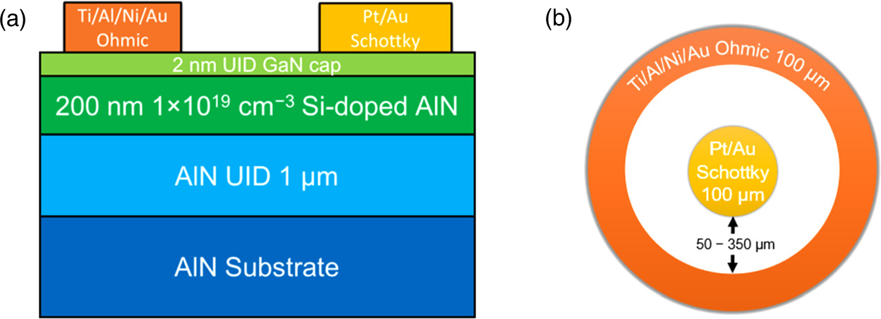
Fig. 1. (a) Schematic of fabricated AlN SBDs on bulk AlN by MOCVD with Ti/Al/Ni/Au Ohmic contact and Pt/Au Schottky contact. (b) Top view of devices.
Download figure:
Standard image High-resolution image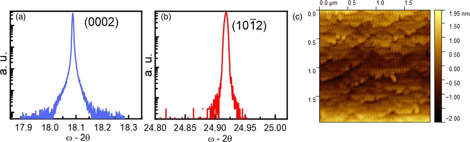
Fig. 2. (a) RCs of  and (b) (
 ) peaks of AlN epilayers by HRXRD. (c) AFM image of the AlN epilayers.
Download figure:
Standard image High-resolution imageFigure 3(a) shows the forward I–V characteristics of the AlN SBDs. The devices showed ON/OFF ratios on the order of 105–106 and turn-on voltage of ∼2.5 V, which are comparable to those of previously reported AlN SBDs. 10–13) The general diode equation for an SBD can be written as 24)


where  is the current density,
  is the saturation current density,
  is the Richardson constant,
  is the temperature in Kelvin,
  is the electron charge,
  is the Schottky barrier height,
  is the ideality factor, and
  is the Boltzmann constant. The Richardson constant used in the calculation was 57.7 Acm−2K−2 using the effective electron mass of 0.48
 11) where
  is the free electron mass. Based on Eqs. (1), and (2), similar Schottky barrier height (
 ) of ∼0.9 eV was obtained for the devices with contact distances of 50, 200, and 350 μm. However, the ideality factor
  varied with increasing distance between Ohmic and Schottky contacts. The minimum value of 4.29 was obtained for the devices with d = 50 μm, which is comparable to previously obtained
  for AlN devices.
12,13) However, other devices with larger contact distances exhibited a slightly larger
for AlN devices.
12,13) However, other devices with larger contact distances exhibited a slightly larger  (6.11 and 7.52 for d = 200 and 350 μm devices, respectively). This indicates that the current transport mechanism is likely to be influenced by surface states and/or resistance of the AlN epilayers due to relatively low carrier concentration. The widely accepted electron affinity of AlN is (χ) 1.9 eV,
25) whereas the work function (
(6.11 and 7.52 for d = 200 and 350 μm devices, respectively). This indicates that the current transport mechanism is likely to be influenced by surface states and/or resistance of the AlN epilayers due to relatively low carrier concentration. The widely accepted electron affinity of AlN is (χ) 1.9 eV,
25) whereas the work function ( ) of Pt is 5.65 eV.
26) The experimental Schottky barrier height obtained in this work deviates from the Schottky–Mott rule,
) of Pt is 5.65 eV.
26) The experimental Schottky barrier height obtained in this work deviates from the Schottky–Mott rule,  owing to Fermi level pinning caused by surface states at the metal/AlN interface.
27) Figure 3(b) shows the I–V curves of AlN SBDs at different temperatures. The devices showed good temperature stability from 298 up to 623 K, and the device ON/OFF ratio increased from 106 to 108 as more carriers contributed to the current transport at higher temperatures.
owing to Fermi level pinning caused by surface states at the metal/AlN interface.
27) Figure 3(b) shows the I–V curves of AlN SBDs at different temperatures. The devices showed good temperature stability from 298 up to 623 K, and the device ON/OFF ratio increased from 106 to 108 as more carriers contributed to the current transport at higher temperatures.
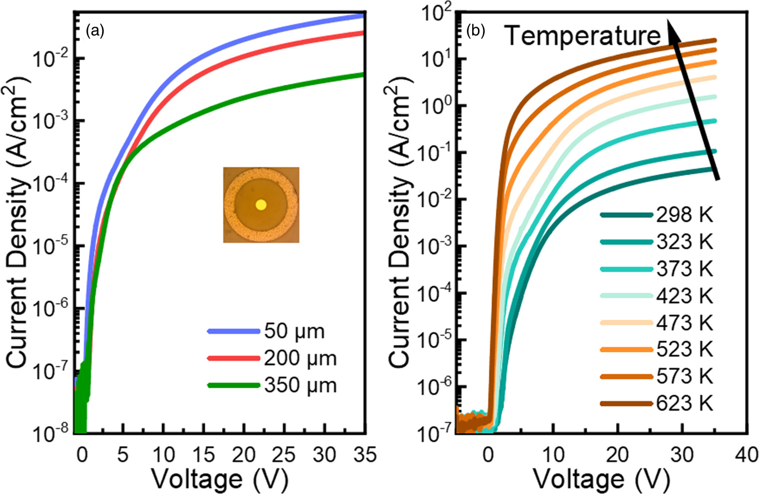
Fig. 3. (a) Forward I–V characteristics of the AlN SBDs with different contact distances on a log scale. Inset: An optical image of fabricated AlN device. (b) Temperature-dependent forward I–V characteristic of the AlN SBDs with a contact distance of 50 μm.
Download figure:
Standard image High-resolution imageFigure 4(a) shows the temperature-dependent  and
and  of the AlN SBD (d = 50 μm). The
  increased from 0.89 to 1.85 eV, and
  decreased from 4.29 to 1.95 with increasing temperature. Figure 4(b) shows a linear relationship between
  and
and  of the devices. This can be ascribed as an inhomogeneous metal/semiconductor interface with distributed low and high Schottky barrier regions.
28,29) In the metal/AlN interface, there are low and high Schottky barrier regions with a Gaussian distribution,
30) originating from non-uniformities under the Schottky metal contact. As a result, at lower temperatures, electrons are limited to passing through regions with lower Schottky barriers. As temperatures increase, electrons gain the energy needed to overcome higher Schottky barrier regions, leading to an increase in the effective
of the devices. This can be ascribed as an inhomogeneous metal/semiconductor interface with distributed low and high Schottky barrier regions.
28,29) In the metal/AlN interface, there are low and high Schottky barrier regions with a Gaussian distribution,
30) originating from non-uniformities under the Schottky metal contact. As a result, at lower temperatures, electrons are limited to passing through regions with lower Schottky barriers. As temperatures increase, electrons gain the energy needed to overcome higher Schottky barrier regions, leading to an increase in the effective  with increasing temperature. This behavior has also been commonly observed in previous reports.
12,13,30) In addition, the devices exhibited behaviors that are more closely aligned with the TE model with increasing temperature, as evidenced by the decreasing
with increasing temperature. This behavior has also been commonly observed in previous reports.
12,13,30) In addition, the devices exhibited behaviors that are more closely aligned with the TE model with increasing temperature, as evidenced by the decreasing  13) This is mainly attributed to the fact that at elevated temperatures more electrons are excited and improved ohmic contacts compared to the RT.
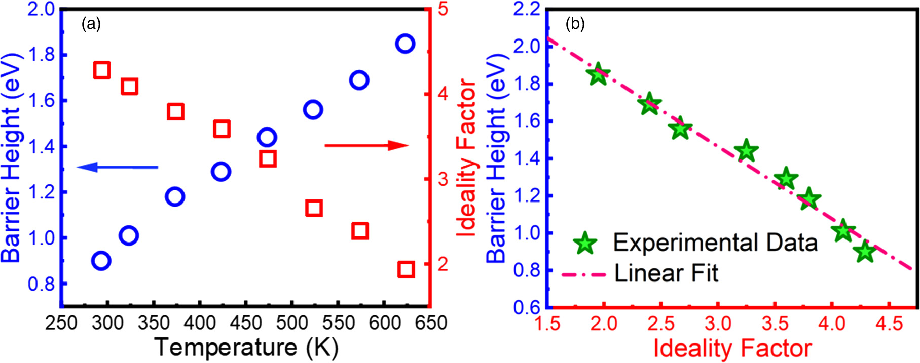
Fig. 4. (a) Ideality factor and Schottky barrier height of the AlN SBDs as a function of temperature. (b) Schottky barrier height versus ideality factor.
Download figure:
Standard image High-resolution image
Fig. 5. (a) C–V plot and 1/C2–V plot at RT for the AlN SBDs. (b) Carrier concertation versus temperature plot. Inset: temperature-dependent C–V measurement of the devices.
Download figure:
Standard image High-resolution imageFurthermore, C–V measurements can be used to extract the carrier concentration of the AlN epilayers using the following equations 24)


where  is the built-in voltage,
  is the permittivity of the vacuum, and
  is the relative permittivity of AlN (
 = 9.2).
31) Figure 5(a) shows the C–V and 1/C2–V plots of the device. C–V measurements of the devices were performed at 10 kHz. The 1/C2–V plot had two regions, corresponding to the AlN UID layer and n-doped AlN, respectively. The extracted carrier concentration of the UID layer was 2.3 × 1016 cm–3, whereas the n-doped region has a carrier concentration of 5.7 × 1017 cm–3, which is much smaller than the Si doping concentration due to dopant compensation
16,18,32,33) and high Si donor ionization energy in AlN (∼250 meV).
16,17,34,35) To better understand the device behavior, temperature-dependent C–V measurements were performed. Figure 5(b) shows temperature-dependent carrier concentration extracted from temperature-dependent C–V measurements of the devices as shown in the inset. As the temperature increased, the carrier concentration varied between 5.7 × 10¹⁷ and 1.6 × 1018 cm–3 from 298 to 623 K. With increasing temperature, more carriers are excited and contribute to the additional capacitance observed.
= 9.2).
31) Figure 5(a) shows the C–V and 1/C2–V plots of the device. C–V measurements of the devices were performed at 10 kHz. The 1/C2–V plot had two regions, corresponding to the AlN UID layer and n-doped AlN, respectively. The extracted carrier concentration of the UID layer was 2.3 × 1016 cm–3, whereas the n-doped region has a carrier concentration of 5.7 × 1017 cm–3, which is much smaller than the Si doping concentration due to dopant compensation
16,18,32,33) and high Si donor ionization energy in AlN (∼250 meV).
16,17,34,35) To better understand the device behavior, temperature-dependent C–V measurements were performed. Figure 5(b) shows temperature-dependent carrier concentration extracted from temperature-dependent C–V measurements of the devices as shown in the inset. As the temperature increased, the carrier concentration varied between 5.7 × 10¹⁷ and 1.6 × 1018 cm–3 from 298 to 623 K. With increasing temperature, more carriers are excited and contribute to the additional capacitance observed.
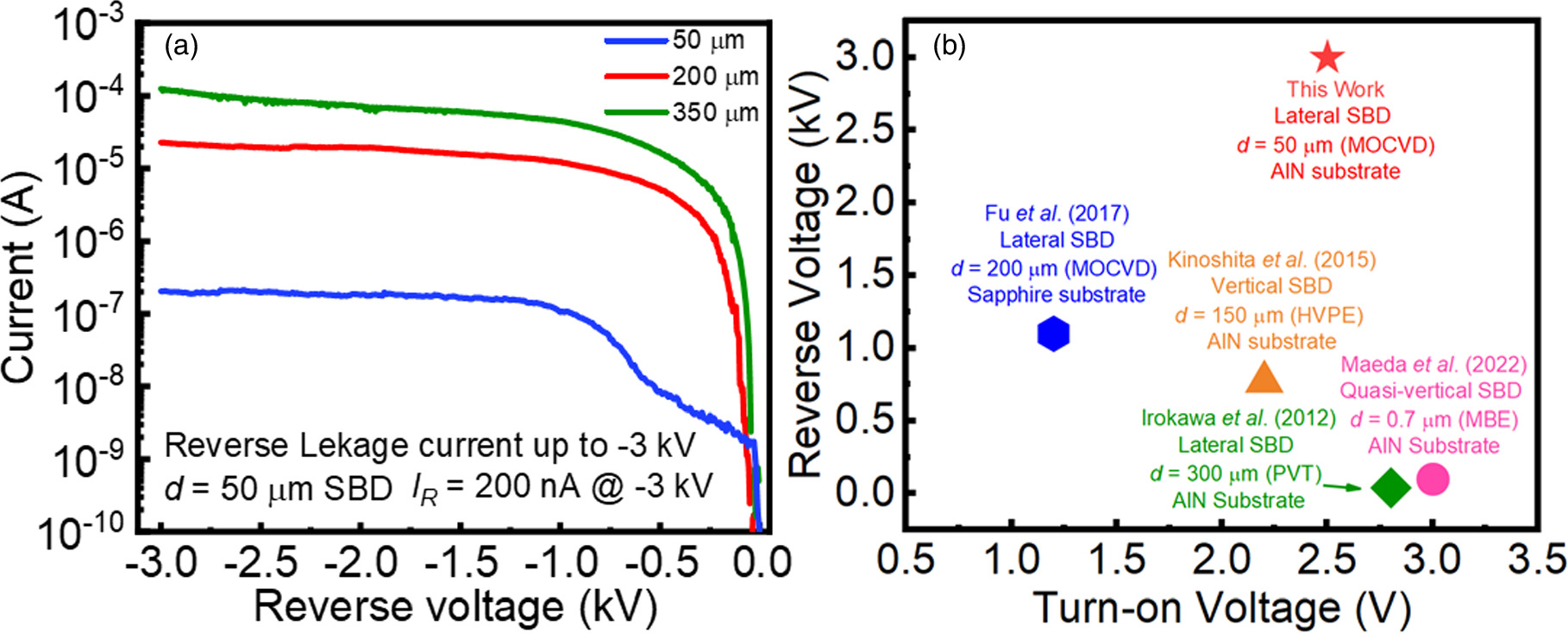
Figure 6(a) shows the reverse I–V characteristics of the AlN SBDs with different contact distances up to −3 kV. All the devices exhibited BV of over 3 kV. It should be noted that no destructive breakdown of the devices was observed up to –3 kV (the limit of the current setup). The reverse leakage current increased with increasing contact distance, and the dominant reverse leakage mechanism warrants further investigation. Reverse leakage can be effectively mitigated through the implementation of passivation and edge termination, which will be explored in future work. Figure 6(b) compares the BV and turn-on voltages of reported AlN SBDs. 10–13) Our work showed record-high BV of over 3 kV with the smallest contact distance and comparable turn-on voltages. The use of AlN bulk substrates in our work resulted in a substantial reduction in defects, paving the way for enhanced device performance compared with our prior work on sapphire substrate. 12)
Fig. 6. (a) Reverse leakage of AlN SBDs. (b) Comparison of the breakdown and turn-on voltages of reported AlN SBDs with the pad distance and growth method.
Download figure:
Standard image High-resolution image
In summary, lateral 3 kV AlN SBDs were grown and fabricated on bulk AlN substrates by MOCVD. The devices showed excellent rectifying behaviors with ON/OFF ratios of 106–108 from 298 to 623 K and good thermal stability. With increasing temperature,  increased from 0.89 to 1.85 eV, while
  decreased from 4.29 to 1.95. These results show the great potential of AlN and serve as an important reference for the future development of multi-kV AlN power electronics.
Acknowledgments
This research is supported as part of ULTRA, an Energy Frontier Research Center funded by the U.S. Department of Energy (DOE), Office of Science, Basic Energy Sciences (BES), under Award # DE-SC0021230. This work is also partially supported by the National Science Foundation (NSF) under Award # 2302696. The authors gratefully acknowledge the use of facilities within the Eyring Center for Solid State Science and ASU NanoFab at Arizona State University.