
Abstract
The magnetization process of a soft magnetic CoFeB-SiO2 thin film was imaged using diamond quantum sensors with perfectly aligned nitrogen-vacancy centers along the [111] direction formed by CVD. Around the film edge, the easy and hard axes directions exhibited different responses to the external magnetic field, consistent with ones observed by magneto-optical Kerr effect microscopy. Moreover, quantum diamond imaging could observe discontinuous magnetization along domain walls as non-uniform magnetic charges (MCs). Quantum diamond imaging would help in visualization through MCs, such as irregularity in the material and relative orientation of magnetizations in neighboring domains.
Export citation and abstract BibTeX RIS

Content from this work may be used under the terms of the Creative Commons Attribution 4.0 license. Any further distribution of this work must maintain attribution to the author(s) and the title of the work, journal citation and DOI.
Soft magnetic thin films are applied to thin-film inductors and tunnel magnetoresistance devices. 1–4) The magnetization–magnetic field (M–H) characteristic, closely related to magnetic anisotropy, permeability, and hysteresis loss, is a key property in all applications. 5) Particularly, unraveling the magnetization process, including local factors such as domain walls and material inhomogeneities, contributes to developing high-performance soft magnetic thin films. The imaging of the magnetization process is performed using magneto-optical Kerr effect (MOKE) microscopy, which is excellent for observing the location of domain walls. 6,7)
Stray field imaging is a superior approach for observing phenomena that can be visualized through magnetic charges (MCs), such as non-uniformity in the material and relative orientation of magnetizations in the neighboring domains. We applied diamond quantum sensors, using nitrogen-vacancy (NV) centers in diamond 8–12) to image the magnetization process with high sensitivity (34 nT·Hz−1/2·μm3/2 is achieved so far). 13–20)
In this study, we demonstrated the imaging of the magnetization process and distribution of MCs in soft magnetic CoFeB-SiO2-thin films. The CoFeB-SiO2 thin film has been developed for HF inductors owing to their low conductivity derived from the structure of nanomagnetic columns dispersed in an insulator matrix. 3) We used perfectly aligned NV centers to image the stray field as a function of the external magnetic field: with unaligned ones, optically detected magnetic resonance (ODMR) dips from multiple crystal axes are concatenated and choosing the best from several candidates of the magnetic field is complicated. We observed the magnetization process along the easy and hard axis, which was consistent with ones observed by MOKE. Moreover, we observed a non-uniform distribution of MC along the domain wall, which is difficult to observe using MOKE.
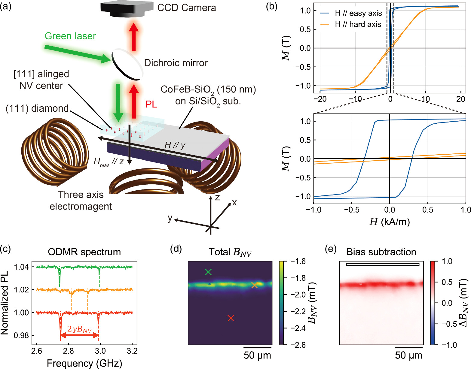
Stray field B from the CoFeB-SiO2 thin film was imaged using NV center-based wide-field diamond sensors as a function of an external magnetic field H [Fig. 1(a)]. The CoFeB-SiO2 thin film was deposited on thermally oxidized silicon substrates with a thickness of 150 nm by facing target sputtering. Detailed fabrication process is described in Ref. 3. Before the NV-based measurement, a macroscopic M–H characteristic was evaluated using a vibrating sample magnetometer (VSM) [Fig. 1(b)]. A high saturation magnetization of approximately 1 T and strong in-plane uniaxial anisotropy was observed. Subsequently, we imaged the magnetization processes for H//the easy axis and H//the hard axis using two rectangular-shaped CoFeB-SiO2 thin films cut out in different directions from one substrate. The direction of the easy (hard) axis was parallel to the y-axis in the lab frame [indicated by arrows in Fig. 1(a)] during the easy (hard) axis measurement. The electromagnet applied a variable magnetic field in the y-direction to drive the magnetization in the film and a fixed magnetic field of approximately 4 mT in the z-direction to resolve the degeneracy of the NV centers. The stray field from the film was imaged based on the ODMR of the NV centers directly glued on the film. Here, the photoluminescence (PL) of the NV centers when a green laser with a wavelength of 532 nm was irradiated was imaged using a CCD camera (Andor iXon3 860). The microwave was applied via a coplanar waveguide resonator with a hole in the middle, which enables uniform and strong microwave irradiation without disturbing the optical path. The distribution of the Rabi frequency was 7.1 ± 0.05 MHz in the resonance condition.

Fig. 1. (a) Overview of the experimental setup. The stray field from soft magnetic CoFeB-SiO2 thin film is imaged by [111] perfectly aligned NV centers while varying the magnetic field controlled by a three-axis electromagnet (bias field//z-axis and variable field//y-axis). The PL from the NV centers when a green laser having a wavelength of 532 nm was irradiated was imaged using a CCD camera. Two types of measurement, H//easy axis or H//hard axis, were performed using CoFeB-SiO2 thin films that were cut out in different directions from one substrate. (b) M–H characteristics of CoFeB-SiO2 evaluated by VSM. The blue and orange lines indicate the in-plane easy axis and in-plane hard axis directions, respectively. (c) ODMR spectra. The selected locations are shown as crosshairs in (d). In most locations, only two dips were observed. The decay of the ODMR contrast at the sample edge can be attributed to a large transverse magnetic field. (d) Magnetic field image before bias subtraction when H = 2300 A m−1 in the hard axis measurement. (e) Magnetic field image after bias subtraction. The black square indicates the reference region. Scales bars are 50 μm in all images.
Download figure:
Standard image High-resolution imageTo effectively observe the stray field from the thin film, the field-of-view (FOV) of the magnetic field imaging was designed to include the magnetic film edge: the edge hosts large MCs and outpours much magnetic flux. The FOV was 158 μm square, and each pixel was 1.2  1.2 μm2 in real space. The spatial resolution was limited by the thickness of the NV layer (1 μm for the easy axis measurement and 5 μm for the hard axis measurement) and the standoff distance between the NV center and the soft magnetic material (expected to be several μm).
We used [111] perfectly aligned NV centers,
21–23) which were deposited by chemical vapor deposition on an Ib (111) substrate, to image the magnetic field. The symmetry axis of the NV center is perfectly aligned perpendicular to the diamond surface. Therefore, only two ODMR dips corresponding to mS = 0 to ±1 transitions were observed throughout the FOV, as shown in Figs. 1(c) and 1(d). The magnetic field  was calculated by dividing the split width of two ODMR dips
  by twice the magnetic rotation ratio
  i.e.
i.e.  Here,
Here,  was calculated by fitting ODMR dips with two Lorentzian functions. Pixels with ill-fitting, where R2 scores less than 0.15, were eliminated [shown as black pixels in Figs. 2 and 3]. On the other hand, the magnetic field calculation would be complicated if we used NV centers with several crystal axes: it is necessary to take correspondence between multiple ODMR dips and the crystal axes of the NV centers, which can change complexly depending on the external and stray fields. Particularly, in the case of degeneracy, taking the correspondence is complicated.
We calculated the stray field by subtracting the bias field from the total magnetic field. The reference region for the bias field was the upper part of the FOV, which is the area outside the magnetic material [Fig. 1(e)].
The magnetization process of the CoFeB-SiO2 thin film along the easy and hard axis was imaged [Fig. 2]. In the easy axis measurement, the external magnetic field was swept from −890 to 700 A m−1, then back to −890 A m−1. We calculated the averaged stray field in the FOV as a function of the external field, equivalent to the M–H characteristic [Fig. 2(a)]. A hysteresis characteristic was observed with a coercive field of ∼±250 A m−1 and a squareness ratio of ∼1, consistent with that measured by VSM [Fig. 1(b)]. Then, we discuss the magnetization process in detail [Fig. 2(c)]. When the magnetization was saturated, the positive MC was concentrated at the edge of the film. The slight distribution of MC was probably caused by the uneven film edges, creating areas where MC tends to concentrate and those where it does not. When the magnetic field was weakened, MCs were distributed in several sharp lines from the edge, and the lines gradually became longer (H = 203 to −95 A m−1). As the magnetic field was further decreased, negative MCs appeared at the edge and inside the film (H < −145 A m−1); only the sharp lines with negative MCs were visible (H = −294 A m−1), and the thin film gradually approached negative magnetic saturation (H < −493 A m−1).
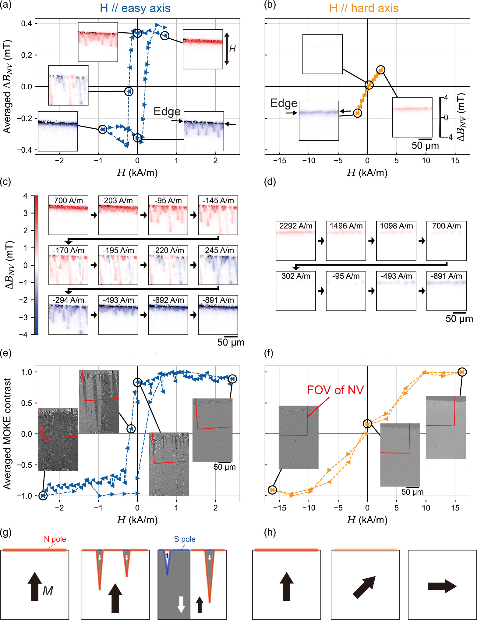
Fig. 2. (a), (b) M–H characteristics in the easy and hard axes, respectively, imaged using wide-field diamond quantum sensors. The horizontal axis represents the external magnetic field. The vertical axis represents the averaged value of the magnetic field in the FOV. The inset shows magnetic field images at several points. (c), (d) Magnetic field images in (a) and (b) when the external field is swept from positive to negative. (e), (f) M–H characteristics along easy and hard axes, respectively, imaged by MOKE. The contrast denotes the longitudinal projection component of the magnetization, normalized to ±1. (g), (h) Estimated mechanism of magnetization process and distribution of MC in the easy and hard axes, respectively. Scales bars are 50 μm in all images.
Download figure:
Standard image High-resolution imageThe hard axis direction exhibited different characteristics from the easy axis [Figs. 2(b) and 2(d)]. The external magnetic field was swept from 2300 to −1700 A m−1, and then back to 2300 A m−1. The M–H characteristic exhibited no apparent hysteresis. The MC was concentrated at the edges for all external field conditions. The non-uniformity of the MCs at the edge of the film was attributed to the unevenness of the film edge, as was the case for the easy axis.
We performed similar measurements using MOKE imaging to ensure the results of the NV centers. Figures 2(e) and 2(f) show the magnetization process along the easy and hard axis, respectively, imaged by longitudinal MOKE imaging. The FOV of the MOKE imaging was almost the same as the NV measurement [red squares in Figs. 2(e) and 2(f)]. Note that this MOKE image was taken independently from the NV images with the diamond removed from the CoFeB-SiO2 film. The contrast denotes the longitudinal projection component of the magnetization. The results of the MOKE support those of the NV centers. M–H characteristics in the easy axis direction demonstrated hysteresis. When the magnetic field was high, the thin film was a single-domain magnet. As the magnetic field decreased, sharp inverse magnetic domains were formed from the edge, the inverse domains expanded through domain wall motion, and the magnetization was entirely reversed. The M–H characteristic in the hard axis showed almost no hysteresis and was almost linear up to approximately ±10 kA m−1. During the magnetization process, no magnetic domains were observed in the FOV of the MOKE imaging.
Considering the NV centers and MOKE results, we discuss the mechanism of the magnetization process and MC distribution in each magnetizing step. In the case of the easy axis direction, the dominant mechanisms in the magnetization process were the formation of inverse magnetic domains at the edges and domain wall motion [Fig. 2(g)]. When the external magnetic field was high, magnetization was positively saturated, and the N-pole MC was concentrated at the edge of the film, where a strong stray field was observed. When the magnetic field decreased slightly, a spike-shaped reverse magnetic domain was formed at the edge of the film. N-pole MCs appeared at the domain wall of the reverse domain, while S-pole MCs appeared at the root of the reverse domain. When the magnetic field decreased further, the reverse magnetic domains grew owing to the domain wall motion, and the spike with the N-pole at the edge appeared. Not all domain walls host MCs: an MC appears if a magnetization next to the domain wall has a perpendicular component to the domain wall. No MC appears if a magnetization is parallel to the domain wall.
In the case of the hard axis direction, the dominant mechanism in the magnetization process is the coherent rotation of magnetization [Fig. 2(h)]. When the external magnetic field is high, magnetization is saturated. When the magnetic field decreases, the magnetization rotates toward the easy axis. The weaker the magnetic field, the fewer MCs the edge hosts. This is because the MC at the edge is proportional to the component of the magnetization perpendicular to the edge. When the external magnetic field is zero, the magnetization turns toward the easy axis, and the MC at the edge becomes zero.
A detailed comparison of results from diamond sensors and MOKE is discussed. 20) To explore the same magnetic field conditions, we plotted M–H characteristics along the easy axis obtained by the NV and MOKE measurements [Fig. 3(a)]. H = −95 A m−1 in the NV and H = −75 A m−1 in the MOKE measurements were selected [circles in Fig. 3(a)]. Both the NV and MOKE measurements indicated that the sharp triangular-shaped reverse magnetic domains were formed from the edge [Fig. 3(b)]. A part of the domain wall of the reverse magnetic domain estimated by the eye is drawn in the NV and MOKE images as dashed lines. The NV image indicates that the MCs are non-uniform along domain walls and form dots, that is, neighboring magnetizations are discontinuous. Moreover, domain walls on the left side of the triangular-shaped domain have larger MCs than those on the right side; magnetizations are asymmetric. These features are difficult to conclude from the MOKE measurement.

Fig. 3. Comparison of the NV and MOKE images. (a) Figs. 2(a) and 2(e) are plotted into one figure to determine the same magnetic field condition. Circular dots are the points selected in (b). (b) NV and MOKE images at almost the same external magnetic field conditions. The dashed lines in the images indicate the domain wall of the reverse magnetic domain estimated by the eye. Scales bars are 50 μm in all images.
Download figure:
Standard image High-resolution image
One of the possible origins for the discontinuous magnetization is scratches on the film surface or strain concentration. One for asymmetric magnetization is the asymmetry of the CoFeB-SiO2 thin film or a misalignment between the CoFeB-SiO2 thin film and the wide-field imaging system. These should be elucidated by observation of the surface morphology using atomic force microscopy, scanning electron microscopy, or nanoscale magnetic imaging using scanning diamond nanoprobes. 24)
In conclusion, we imaged the magnetization process of the CoFeB-SiO2 thin film using wide-field diamond quantum sensors. Discontinuous magnetization along domain walls was detected as a non-uniform MC, which is challenging to observe in the MOKE measurement. Diamond quantum imaging helps evaluate material properties that can be visualized through MCs, such as non-uniformity in the material and relative orientation of magnetizations in neighboring domains. Using both NV measurements, which are effective in estimating the location and amount of MC, and MOKE measurements, which are effective in estimating the location of domain walls, will enable a more comprehensive characterization of materials.
Acknowledgments
This study was supported by the MEXT Quantum Leap Flagship Program (MEXT Q-LEAP) Grant No. JPMXS0118067395 and JST SPRING Grant No. JPMJSP2106.