 01), (001), and (010) crystal orientations
Abstract
NiOx/β-Ga2O3p-n heterojunctions fabricated on 
 and
and  β-Ga2O3 substrates show distinctly anisotropic electrical properties. All three devices exhibited excellent rectification ≥109, and turn-on voltages >2.0 V. The
  device showed very different turn-on voltage, specific on-resistance, and reverse recovery time compared with
  and
and  devices. Moreover, it is calculated that the interface trap state densities for
 and
and  plane devices are 4.3 × 10¹⁰, 7.4 × 10¹⁰, and 1.6 × 10¹¹ eV–1cm–2, respectively. These differences in the NiOx/β-Ga2O3 heterojunctions are attributed to the different atomic configurations, the density of dangling bonds, and interface trap state densities.
Export citation and abstract BibTeX RIS
There has been substantial recent interest in ultra-wide bandgap (UWBG) semiconductors, such as gallium oxide (β-Ga2O3), 1) aluminum nitride, 2) diamond, 3) and boron nitride 4) for power electronics due to their large bandgaps and high critical field. These properties can result in higher operating voltages, larger currents, increased efficiencies, and smaller device footprint compared to devices based on traditional semiconductors such as silicon and wide bandgap semiconductors such as silicon carbide and gallium nitride. 5) As an emerging UWBG material, β-Ga2O3 has attracted much attention for electronic and photonic device applications. 1) However, a significant challenge for β-Ga2O3 is its lack of p-type conductivity. Theoretical predictions indicate a difficulty in obtaining holes due to the high activation energy (>1 eV) of acceptors for β-Ga2O3. 6) Moreover, due to the flat valence band maximum, the heavy hole effective mass leads to low hole mobility 7) while holes tend to be localized in β-Ga2O3 as polarons due to lattice distortion. 8) Thus, most reported β-Ga2O3 devices, such as field effect transistors 9) and Schottky barrier diodes, 10) are unipolar. The demonstration of p-n junctions in β-Ga2O3 is critical for the development of bipolar devices and advanced Ga2O3-based electronic devices.
Recently, p-NiOx has emerged as a popular choice for the formation of β-Ga2O3 p-n heterojunctions due to its easy deposition and extensive use as a hole contact in high-efficiency solar cells. 11,12) Kokubun et al. 13) demonstrated the first NiOx /β-Ga2O3 p-n heterojunction with Li-doped NiOx epitaxial layer. Several NiOx /β-Ga2O3 heterojunctions, including p-n diodes 14–16) and junction barrier Schottky diodes 17–19) have been demonstrated with excellent electrical characteristics, such as low on-resistance, high on/off ratio, and large reverse blocking voltage. Moreover, NiOx /β-Ga2O3 heterojunctions are versatile with a wide range of applications, including edge terminations in β-Ga2O3 power diodes 20) and all-oxide-based UV photodetectors. 21)
The low crystal symmetry of monoclinic β-Ga2O3 results in highly anisotropic material with a direct impact on several key physical and electronic properties, such as dielectric constant,
22) thermal conductivity,
23) and electron mobility
24) which are different along different crystallographic directions. This anisotropy poses challenges for device fabrication and results in discrepancies in device performance. Fu et al.
24) compared Schottky contacts on  and
and  β-Ga2O3 planes and observed that the
  orientation had higher barrier height and lower reverse leakage. Sasaki et al.
25) reported that the rate of epitaxial growth on the
orientation had higher barrier height and lower reverse leakage. Sasaki et al.
25) reported that the rate of epitaxial growth on the  plane was slower compared to the
  plane due to the low adhesion energy on
  terraces. Jang et al.
26) found that the etch rate and ability to form Ohmic contacts on
terraces. Jang et al.
26) found that the etch rate and ability to form Ohmic contacts on  plane was higher compared to
  plane owing to the higher density of oxygen dangling bonds. However, the anisotropic properties of the widely used NiOx
/β-Ga2O3 heterojunctions are not well understood. In this work, a systematic comparative analysis of NiOx
/β-Ga2O3
p-n heterojunctions with
plane owing to the higher density of oxygen dangling bonds. However, the anisotropic properties of the widely used NiOx
/β-Ga2O3 heterojunctions are not well understood. In this work, a systematic comparative analysis of NiOx
/β-Ga2O3
p-n heterojunctions with 
 and
and  substrate orientations has been carried out. Temperature-dependent electrical measurements, reverse recovery characteristics, and capacitance–frequency (C–f) measurements, were performed to provide a better understanding of the anisotropic nature of NiOx
/β-Ga2O3
p-n heterojunctions.
substrate orientations has been carried out. Temperature-dependent electrical measurements, reverse recovery characteristics, and capacitance–frequency (C–f) measurements, were performed to provide a better understanding of the anisotropic nature of NiOx
/β-Ga2O3
p-n heterojunctions.
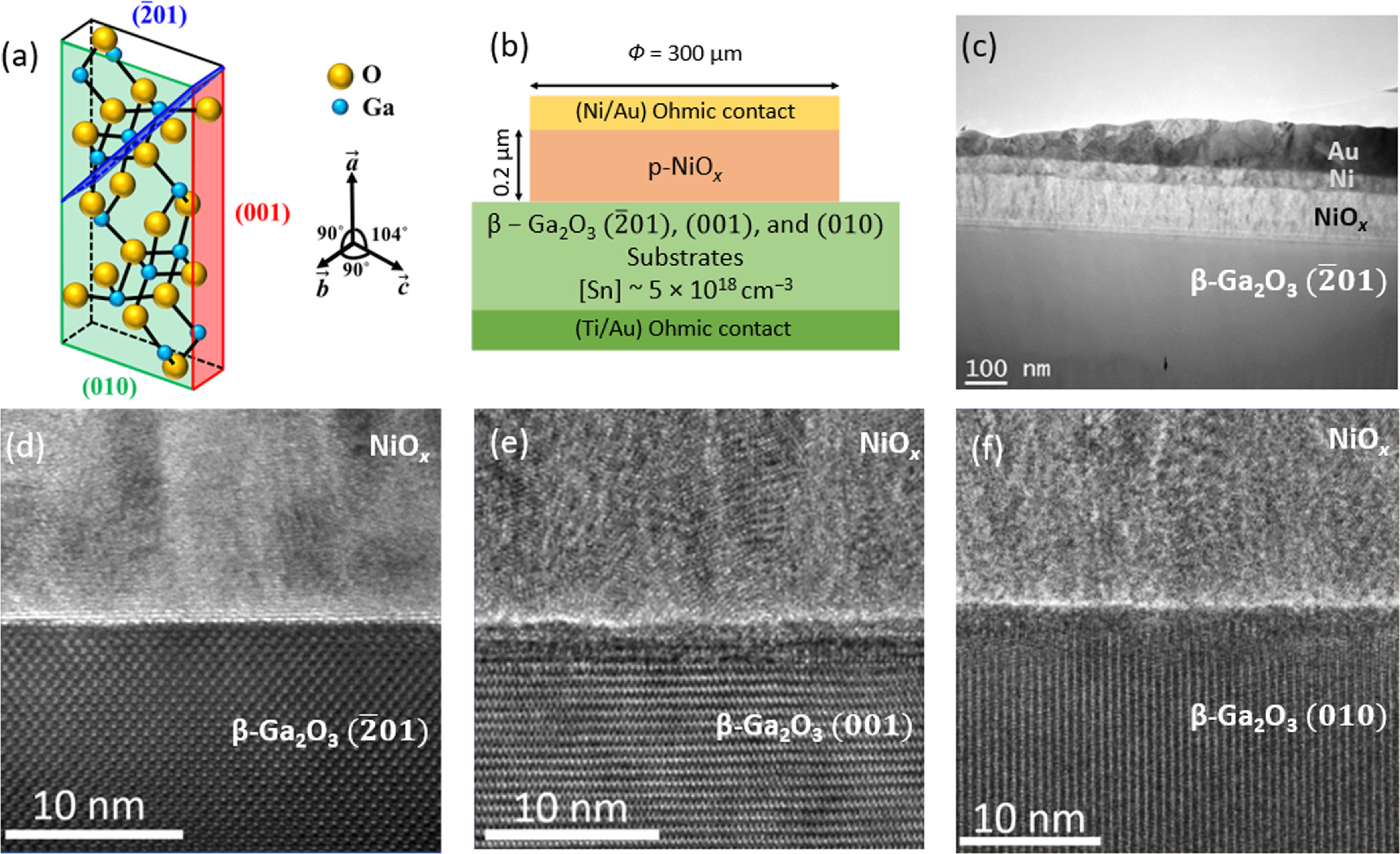
Figure 1(a) shows the crystal structure of β-Ga2O3 and the corresponding planes used as substrates for this study. These β-Ga2O3 planes are widely used for β-Ga2O3 devices. Previous literature has shown clear differences between  [or
[or  ] and
] and  plane dangling bond densities, which were calculated to be 2.68 × 10¹⁵ [or 2.69 × 10¹⁵] and 1.74 × 1015 cm–2, respectively.
27) Edge-defined film-fed grown
plane dangling bond densities, which were calculated to be 2.68 × 10¹⁵ [or 2.69 × 10¹⁵] and 1.74 × 1015 cm–2, respectively.
27) Edge-defined film-fed grown 
 and
and  β-Ga2O3 substrates from Novel Crystal Technology were used for this study.
28) The substrates had similar n-type [Sn] doping concentrations of ∼5 × 1018 cm−3, similar thickness, and good crystalline quality, as verified by XRD measurements. To prepare the substrates, a standard cleaning procedure was implemented, which included cleaning with acetone, isopropyl alcohol, and deionized water, aided by sonication. The back contacts of Ti/Au (20/130 nm) were deposited using electron beam (E-beam) evaporation. followed by rapid thermal annealing at 500 °C in an N2 environment. All back contacts showed very low contact resistance of <0.01 mΩcm2. Standard photolithography was then performed to define circular patterns for the deposition of NiOx
and the anode (diameter of 300 μm). 200 nm NiOx
and the anode Ni/Au (20/130 nm) were deposited using E-beam evaporation, followed by a lift-off process. The fabricated device structure and device dimensions are shown in Fig. 1(b). The anode, cathode, and NiOx
layers were deposited simultaneously for all samples to avoid any inconsistencies in fabrication. All NiOx
layers were highly doped with a similar hole density of >2 × 18 cm–3, and the Ohmic contacts to NiOx
layers had a similar contact resistance of ∼0.3 mΩcm2. After device fabrication, all samples were annealed at 350 °C in N2 ambient for 1 min. This annealing step was expected to improve the device performance by forming an Ohmic contact between the Ni/NiOx
interface and reducing the number of interface states at the NiOx
/β-Ga2O3 heterojunction.
29)
β-Ga2O3 substrates from Novel Crystal Technology were used for this study.
28) The substrates had similar n-type [Sn] doping concentrations of ∼5 × 1018 cm−3, similar thickness, and good crystalline quality, as verified by XRD measurements. To prepare the substrates, a standard cleaning procedure was implemented, which included cleaning with acetone, isopropyl alcohol, and deionized water, aided by sonication. The back contacts of Ti/Au (20/130 nm) were deposited using electron beam (E-beam) evaporation. followed by rapid thermal annealing at 500 °C in an N2 environment. All back contacts showed very low contact resistance of <0.01 mΩcm2. Standard photolithography was then performed to define circular patterns for the deposition of NiOx
and the anode (diameter of 300 μm). 200 nm NiOx
and the anode Ni/Au (20/130 nm) were deposited using E-beam evaporation, followed by a lift-off process. The fabricated device structure and device dimensions are shown in Fig. 1(b). The anode, cathode, and NiOx
layers were deposited simultaneously for all samples to avoid any inconsistencies in fabrication. All NiOx
layers were highly doped with a similar hole density of >2 × 18 cm–3, and the Ohmic contacts to NiOx
layers had a similar contact resistance of ∼0.3 mΩcm2. After device fabrication, all samples were annealed at 350 °C in N2 ambient for 1 min. This annealing step was expected to improve the device performance by forming an Ohmic contact between the Ni/NiOx
interface and reducing the number of interface states at the NiOx
/β-Ga2O3 heterojunction.
29)

Fig. 1. (a) Monoclinic crystal structure of β-Ga2O3 with crystal planes of 
 and
and  labeled. (b) Schematic of fabricated NiOx
/β-Ga2O3
p-n heterojunctions. (c) TEM image of the interfaces of NiOx
/β-Ga2O3 heterojunctions fabricated on
labeled. (b) Schematic of fabricated NiOx
/β-Ga2O3
p-n heterojunctions. (c) TEM image of the interfaces of NiOx
/β-Ga2O3 heterojunctions fabricated on  plane. HRTEM images of the NiOx
/β-Ga2O3 interface of (d)
plane. HRTEM images of the NiOx
/β-Ga2O3 interface of (d)  (e)
(e)  and (f)
  devices.
Download figure:
Standard image High-resolution imageElectrical characterization was conducted using a probe station equipped with a controllable thermal chuck, Keithley 4200-SCS parameter analyzer, and ultra-fast pulse measurement units. Cross-sectional transmission electron microscope (XTEM) images were taken for all samples. The TEM samples were prepared using a Thermo Fisher Helios 5UX Dualbeam system with final thinning in a Gatan precision ion-polishing system. The milling started with a Ga-focused ion beam at 30 keV, followed by thinning at 5 and 2 keV, and subsequent Ar-ion thinning at 2 and 1 keV. Devices with 
 and
and  β-Ga2O3 substrate normals were imaged along their respective [010], [100] and [001] zone axes. High-resolution TEM (HRTEM) images were taken using a Philips CM 200 operated at 200 kV and an image-corrected FEI Titan 80–300 operated at 300 kV. Figure 1(c) shows an XTEM image of the full diode structure consisting of the top electrode (Au, Ni), NiOx, and β-Ga2O3 substrate. Figures 1(d)–1(f) show HRTEM images of the NiOx
/β-Ga2O3 interface for samples grown on
β-Ga2O3 substrate normals were imaged along their respective [010], [100] and [001] zone axes. High-resolution TEM (HRTEM) images were taken using a Philips CM 200 operated at 200 kV and an image-corrected FEI Titan 80–300 operated at 300 kV. Figure 1(c) shows an XTEM image of the full diode structure consisting of the top electrode (Au, Ni), NiOx, and β-Ga2O3 substrate. Figures 1(d)–1(f) show HRTEM images of the NiOx
/β-Ga2O3 interface for samples grown on 
 and
and  substrates, respectively. The polycrystalline nature of NiOx
layers was evident in HRTEM images, and abrupt NiOx
/β-Ga2O3 interfaces were clearly visible.
substrates, respectively. The polycrystalline nature of NiOx
layers was evident in HRTEM images, and abrupt NiOx
/β-Ga2O3 interfaces were clearly visible.
Figure 2(a) shows I–V curves for the three NiOx
/β-Ga2O3
p-n diodes, where the turn-on voltages were 2.09, 2.22, and 2.50 V for 
 and
and  substrates, respectively. Devices on
  and
and  planes had excellent rectification ratios of ∼1010 at ±3.75 V. However,
  devices showed a smaller on/off ratio of about ∼109 at ±3.75 V. Furthermore, devices on
  and
and  planes exhibited specific on-resistances of 2.92 and 1.55 mΩcm2, while the
  device showed a specific on-resistance of 6.50 mΩcm2. Ideality factors were 1.95, 2.03, and 2.13 for
 and
and  planes, respectively. These large ideality factors indicate that the current recombination in the heterojunction is dominant compared to diffusion currents.
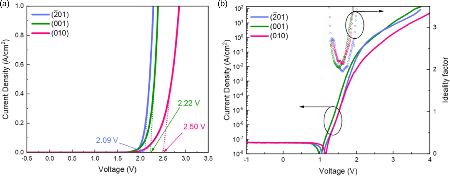
Fig. 2. I–V characteristics of NiOx /β-Ga2O3 p-n heterojunctions on three crystallographic orientations: (a) linear scale and (b) semi-log scale.
Download figure:
Standard image High-resolution imageThe C–V measurements were performed at a frequency of 100 kHz [Fig. 3(a)], and the devices showed built-in potentials of 2.72, 2.74, and 2.63 V on 
 and
and  devices, respectively [Fig. 3(b)]. The built-in voltages were comparable in all three devices since there is no current transport through the devices in C–V measurements. The built-in voltages determined by I–V and C–V measurements showed some discrepancies. In general, C–V measurements are mainly affected by the doping concentration of NiOx
and β-Ga2O3, as well as the charges from the interface states. However, they do not provide information about the current conduction through the interface. Conversely, extraction of built-in voltage through I–V measurements is influenced by the crystal anisotropy and interface states. The effective carrier concentration (
devices, respectively [Fig. 3(b)]. The built-in voltages were comparable in all three devices since there is no current transport through the devices in C–V measurements. The built-in voltages determined by I–V and C–V measurements showed some discrepancies. In general, C–V measurements are mainly affected by the doping concentration of NiOx
and β-Ga2O3, as well as the charges from the interface states. However, they do not provide information about the current conduction through the interface. Conversely, extraction of built-in voltage through I–V measurements is influenced by the crystal anisotropy and interface states. The effective carrier concentration ( )
30) calculated from the C–V measurements was 4.7 × 10¹⁸, 4.5 × 10¹⁸, 1.6 × 1018 cm–3 for
)
30) calculated from the C–V measurements was 4.7 × 10¹⁸, 4.5 × 10¹⁸, 1.6 × 1018 cm–3 for 
 and
and  devices, respectively, where
  is the ionized donor concentration,
  is the ionized acceptor concentration, and
  is the equivalent charge concentration of traps. Since the β-Ga2O3 and NiOx
film in the three samples had similar carrier concentrations, the observed variation in the effective carrier concentrations is likely related to the different NiOx
/β-Ga2O3 heterojunction interfaces caused by the crystal anisotropy, which is verified by C–f measurements.
is the equivalent charge concentration of traps. Since the β-Ga2O3 and NiOx
film in the three samples had similar carrier concentrations, the observed variation in the effective carrier concentrations is likely related to the different NiOx
/β-Ga2O3 heterojunction interfaces caused by the crystal anisotropy, which is verified by C–f measurements.

Fig. 3. (a) C–V measurements, and (b) 1/C2
–V plots of NiOx
/β-Ga2O3
p-n heterojunctions for three crystallographic orientations. The C–f characteristics with corresponding fitting curves for devices on (c)  (d)
(d)  and (e)
  planes.
Download figure:
Standard image High-resolution imageFigures 3(c)–3(e) show C–f measurements for the devices on 
 and
and  substrates to evaluate the interface trap state density (
 ). The C–f measurements are fitted using the equations below, assuming the interface states are distributed in two energy levels.
31,32)
). The C–f measurements are fitted using the equations below, assuming the interface states are distributed in two energy levels.
31,32)


where  is the capacitance of the space charge region, and
  (
( ) is the capacitance of the first state (second state) with their corresponding relaxation time
  (
( ).
).  represents an energy level that corresponds to interface states closer to the conduction band with a smaller relaxation time, and
  represents a deep energy level with a considerably larger relaxation time. A similar
  of ∼2 × 10⁻¹² F was observed with a relaxation time of about ∼8 μs for all devices. This may represent deep-level states (e.g., vacancies) with relaxation time much larger than the interface states. However,
  varied significantly for devices on different crystal orientations. The relaxation time for
  was 0.64, 0.43, and 0.34 μs for
 and
and  devices, respectively, which are consistent with previous reports.
31,32)
devices, respectively, which are consistent with previous reports.
31,32)
 changed with crystal orientation, while
  remained relatively constant. It should be noted that the exact nature of the defect states in NiOx
/β-Ga2O3 diodes is still unclear and demands further investigation. The extracted interface trap densities (
remained relatively constant. It should be noted that the exact nature of the defect states in NiOx
/β-Ga2O3 diodes is still unclear and demands further investigation. The extracted interface trap densities ( ) from
  were 4.3 × 10¹⁰, 7.4 × 10¹⁰, and 1.6 × 10¹¹ eV–1cm–2 for
 and
and  devices, respectively.
29,31,32) The interface states derived from
devices, respectively.
29,31,32) The interface states derived from  are much closer to the conduction band, and thus may play an important role in the device performance. Table I summarizes all the parameters extracted through C–f curve fitting.
Table I. Interface state parameters extracted from C–f curve fitting.
| Orientation |
 (F) (F) |
 (F) (F) |
 (s) (s) |
 (s) (s) |
 (eV–1cm–2) (eV–1cm–2) |
 (eV–1cm–2) (eV–1cm–2) |
|---|---|---|---|---|---|---|

| 4.80 × 10⁻¹² | 2.50 × 10⁻¹² | 0.64 × 10⁻⁶ | 8.69 × 10⁻⁶ | 4.3 × 10¹⁰ | 2.2 × 10¹⁰ |

| 8.36 × 10⁻¹² | 2.27 × 10⁻¹² | 0.43 × 10⁻⁶ | 8.57 × 10⁻⁶ | 7.4 × 10¹⁰ | 2.0 × 10¹⁰ |

| 1.79 × 10⁻¹¹ | 1.62 × 10⁻¹² | 0.34 × 10⁻⁶ | 8.02 × 10⁻⁶ | 1.6 × 10¹¹ | 1.4 × 10¹⁰ |
The differences in electrical properties of NiOx
/β-Ga2O3
p-n heterojunctions can be attributed to several factors. First, the difference in interface states may be significantly promoted by the density of dangling bonds. If the number of dangling bonds is high, then the adhesion of the NiOx
layer is promoted, exhibiting fewer interface states. Due to the higher dangling bond density in  and
and  plane, it is easier to form better-quality NiOx
/β-Ga2O3 heterojunction with high surface energy.
27) This is analogous to the fact that forming Ohmic contacts on
plane, it is easier to form better-quality NiOx
/β-Ga2O3 heterojunction with high surface energy.
27) This is analogous to the fact that forming Ohmic contacts on  and
and  planes is easier than on
  plane.
26) Second, different doping concentrations can be induced in the heterojunction due to interface states. The interface states can have a big impact on net charge density. It is likely that there are lower compensating trap states in
plane.
26) Second, different doping concentrations can be induced in the heterojunction due to interface states. The interface states can have a big impact on net charge density. It is likely that there are lower compensating trap states in  and
and  NiOx
/β-Ga2O3
p-n heterojunctions as indicated by the C–f measurement, contributing larger net charge densities. This is further evidenced by the different gradients in the 1/C2
–V plot. The observed differences are primarily influenced by the presence of interface states, considering three NiOx
and β-Ga2O3 in the three samples had similar carrier concentrations. As discussed later, a difference in reverse recovery time (
NiOx
/β-Ga2O3
p-n heterojunctions as indicated by the C–f measurement, contributing larger net charge densities. This is further evidenced by the different gradients in the 1/C2
–V plot. The observed differences are primarily influenced by the presence of interface states, considering three NiOx
and β-Ga2O3 in the three samples had similar carrier concentrations. As discussed later, a difference in reverse recovery time ( ) of the devices was observed, indicating that carrier recombination on different planes is affected by the crystal anisotropy.
The temperature-dependent forward characteristics of three NiOx
/β-Ga2O3
p-n diodes are presented in Figs. 4(a)–4(c). The observed temperature-dependent behavior was stable and reproducible, and the initial I–V curves were retained even after heating and cooling down, indicating excellent thermal stability of the heterojunction.
16,29) The device ideality factor and turn-on voltage were extracted as a function of temperature, as shown in Figs. 4(d)–4(f). The turn-on voltage decreased linearly with the temperature, which can be attributed to the reduction of depletion width facilitating diffusion of holes.
33) The ideality factor varied between 1.95–3.77, 2.03–2.95, and 2.13–4.47 in 
 and
and  devices, respectively. This behavior of turn-on voltage and ideality factor is consistent with previous reports.
29,33) The ideality factor of
devices, respectively. This behavior of turn-on voltage and ideality factor is consistent with previous reports.
29,33) The ideality factor of  and
and  devices remained almost constant under high temperatures. However, the ideality factor in
  devices first increased and then decreased. This behavior can be attributed to the fact that there are 10 times more interface trap states in
  heterojunction compared to
  and
and  heterojunctions. With increasing temperature, the carrier emission from interface traps is enhanced, affecting the ideality factor.

Fig. 4. Temperature-dependent I–V curves for the devices on (a)  (b)
(b)  and (c)
  . Variation of turn-on voltage and ideality factor of corresponding I–V curves are shown in (d), (e), and (f).
Download figure:
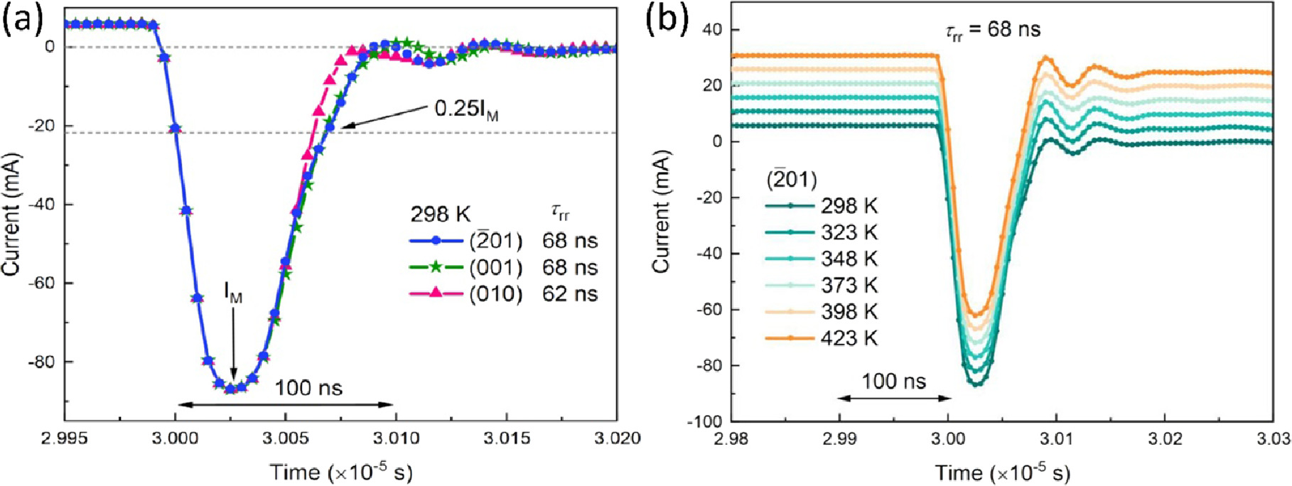
Standard image High-resolution imageThe  of the diode is defined as the time it takes to reach 0.25
 after switching off, where
  is the maximum current during the reverse recovery period. The
  of the diodes is affected by several factors, including the doping concentration, the width of the depletion region, crystal anisotropy, and the applied voltage. In this work, all three samples were subject to voltages of ±5 V to observe the reverse recovery of the diode. The
  and
and  devices had a
  of 68 ns, while (010) devices took 62 ns to recover [Fig. 5(a)]. The shorter reverse recovery time for
  is likely due to larger interface defect densities that promote electron/hole recombination with a faster recovery time and mobility variation along different crystal orientations. All devices had a peak current of about 86 mA and showed temperature independence
33) in reverse recovery time, as shown in Fig. 5(b), where the y-axis is offset for clarity. This indicates that the junction capacitance and stored charges in the depletion region are independent of temperature. The forward current during the reverse recovery test was ∼6 mA. Additionally, the
is likely due to larger interface defect densities that promote electron/hole recombination with a faster recovery time and mobility variation along different crystal orientations. All devices had a peak current of about 86 mA and showed temperature independence
33) in reverse recovery time, as shown in Fig. 5(b), where the y-axis is offset for clarity. This indicates that the junction capacitance and stored charges in the depletion region are independent of temperature. The forward current during the reverse recovery test was ∼6 mA. Additionally, the  of three samples for the reverse recovery characteristics was 3.95 A μs−1, which is comparable to previously reported values.
33) The reverse recovery charge was 4.47, 4.54, and 4.26 nC for
of three samples for the reverse recovery characteristics was 3.95 A μs−1, which is comparable to previously reported values.
33) The reverse recovery charge was 4.47, 4.54, and 4.26 nC for 
 and
and  devices, respectively. The different
  in different crystal orientations indicate carrier recombination is influenced by the interface states. Table II summarizes the device parameters of the three NiOx
/β-Ga2O3
p-n heterojunctions, where
in different crystal orientations indicate carrier recombination is influenced by the interface states. Table II summarizes the device parameters of the three NiOx
/β-Ga2O3
p-n heterojunctions, where  of the devices is based on the dominant
  values.
Fig 5. (a) Reverse recovery of NiOx
/β-Ga2O3
p-n heterojunctions on three crystallographic orientations. (b) Temperature-dependent reverse recovery of p-n diodes on  plane.
Download figure:
Standard image High-resolution image
Table II. Electrical properties of the NiOx
/β-Ga2O3
p-n diode heterojunctions grown on 
 and
and  substrates.
| Orientation | Von(I–V) (V) | Vbi(C–V) (V) | Rsp-on(mΩcm2) | on/off ratio | η |
 (ns) (ns) |
 (eV–1cm–2) (eV–1cm–2) |
|---|---|---|---|---|---|---|---|

| 2.09 | 2.74 | 2.92 | 1010 | 1.95 | 68 | 4.3 × 10¹⁰ |

| 2.22 | 2.72 | 1.55 | 1010 | 2.03 | 68 | 7.4 × 10¹⁰ |

| 2.50 | 2.63 | 6.50 | 109 | 2.13 | 62 | 1.6 × 10¹¹ |
In conclusion, NiOx
/β-Ga2O3
p-n heterojunctions fabricated on 
 and
and  substrates showed considerable differences in electrical properties in terms of turn-on voltages, ideality factor, on-resistance, and reverse recovery time. The (010) device exhibited the highest turn-on voltage of 2.50 V, the highest ideality factor of 2.13, the largest on-resistance of 6.50 mΩcm2, and the lowest recovery time of 62 ns. The C–f measurements indicate an interface trap density of 4.3 × 10¹⁰, 7.4 × 10¹⁰, and 1.6 × 10¹¹ eV–1cm–2 for
 and
and  plane devices, respectively. All devices were fabricated simultaneously and exhibited excellent rectifying behaviors with a high on/off ratio of ≥109 and high-quality interfaces between NiOx
and β-Ga2O3, as confirmed by HRTEM. These differences in device electrical properties are attributed to the different atomic configurations, the density of dangling bonds, and interface trap state densities. These results indicate the anisotropic nature of β-Ga2O3 in heterojunction-based p-n diodes and should serve as a valuable reference for future development of Ga2O3 heterojunction bipolar devices.
plane devices, respectively. All devices were fabricated simultaneously and exhibited excellent rectifying behaviors with a high on/off ratio of ≥109 and high-quality interfaces between NiOx
and β-Ga2O3, as confirmed by HRTEM. These differences in device electrical properties are attributed to the different atomic configurations, the density of dangling bonds, and interface trap state densities. These results indicate the anisotropic nature of β-Ga2O3 in heterojunction-based p-n diodes and should serve as a valuable reference for future development of Ga2O3 heterojunction bipolar devices.
Acknowledgments
This research is supported as part of ULTRA, an Energy Frontier Research Center funded by the U.S. Department of Energy (DOE), Office of Science, Basic Energy Sciences (BES), under Award # DE-SC0021230. This work is also partially supported by the National Science Foundation (NSF) under Award # 2302696. The authors also acknowledge the use of facilities within the John M. Cowley Center for High Resolution Electron Microscopy at Arizona State University, supported in part by NSF grant ECCS-2025490.