

Abstract
In the manufacture of power devices, ion implantation into gallium nitride (GaN) to a depth of several microns is a challenge because the activation of such devices is disturbed by the damage caused by implantation. To reduce this damage, a channeled implantation technique was applied to implant magnesium (Mg) ions into GaN (0001). Compared with random implantation, channeled implantation showed implantation and activation of ions in regions up to an order of magnitude deeper. Channeled ion simulation code developed herein successfully reproduced the experimental values, thus enabling the application of this technology to process a power device using GaN.
Export citation and abstract BibTeX RIS
Vertical gallium nitride (GaN) power devices are highly efficient for power conversion systems. 1–12) However, they rely on complicated etching and regrowth processes. Preferably, a simple planar process based on ion implantation, as used in silicon and silicon carbide devices, could be developed for GaN device fabrication. 13) The fabrication of vertical power devices using ion implantation requires doping to a deep layer with little damage. Attempts were made until around 2002 to create p-type GaN through ion implantation but were unsuccessful. 14) To the best of our knowledge, there has been only one attempt at channeled implantation, but its activation results were not reported. 15) Since 2014, improvements in GaN substrate quality and annealing techniques have led to renewed attempts to fabricate p-type GaN through ion implantation. 16,17) The ultrahigh-pressure-annealing (UHPA) method, which can anneal at temperatures of 1300 °C or higher using pressurized nitrogen gas, has been devised and confirmed as a method for producing p-type films meeting the same requirements as epitaxial films. 18) It has also been reported that the UHPA method can be used to activate the material even after prolonged annealing at 1200 °C. 19) Annealing at such a high temperature is necessary to repair the many point defects introduced into the implantation layer under random implantation conditions. 20) In our previous work, we attempted channeled implantation of Mg ions into GaN in hopes of reducing the number o.f defects and activating the material at temperatures below 1200 °C. 21) Channeled implantation was found to reduce the number of defects by reducing the likelihood that incident ions collide with atoms in the sample. In addition, since the incident ions pass through the hexagonal channel centers, they are less likely to lose energy and thus should implant into relatively deep layers. Our results showed that Mg ions could be implanted into deep layers of GaN under channeled implantation conditions, and a clear donor–acceptor pair signal, which is one indicator of activation, was observed even from deep layers at annealing temperatures below 1200 °C.
To apply this technology to device fabrication, it is necessary to be able to reproduce the implantation distribution via simulation. For this purpose, we have developed code (scatGUI), posted at 〈https://www.hosei.ac.jp/ionbeam_e/software/scatgui/〉, simulating ion trajectories passing through a crystal lattice. In this paper, we show that the code can reproduce the implantation distribution across a range of doses. In particular, for high-dose implantation, we show that defects generated during implantation affect the implantation distribution. We further show that the implantation distribution for high doses can be reproduced by incorporating the effect of defect generation into the simulation.
Implantation simulation has been performed in many studies over many years, and many code modules have been developed. 22–25) For example, SRIM 22) is used to calculate random implantation distributions, and Crystal-TRIM, 23) MARLOWE, 24) and Sentaurus MD 25) are used to calculate implantation distributions for crystals. Simulations of implantation to GaN using the MARLOWE code have also been performed. 26) The code developed herein is a modified version of a code module used for ion scattering analysis. 27) A graphical user interface was also developed and released as a program for easily setting the parameters for channeled implantation of ions into GaN. 28) The calculation method is based on the two-body collision approximation as is typical in the code modules described above. The target is assumed to be a thermally vibrating atom in a crystal, and the calculation is based on a Monte Carlo simulation in which the trajectories of tens of thousands of incident ions are calculated until they stop. (In the present calculation, each ion is judged to have stopped when its energy drops below 3 eV.)
Our simulation's main differentiators and features are as follows. (A) The standard stopping power value is based on Ziegler et al.
22,29) and can be set by magnification if necessary. (B) We use the following equation for impact-parameter-dependent electronic stopping power, based on Oen and Robinson's stopping power:
30)
 where Se,Ziegler (E) (eV cm−2) is the Ziegler's electronic stopping power, b (cm) is the impact parameter, am is the Molière's screening radius,
30) and β is a coefficient whose original value of 0.3
31) can be changed. Another feature of our program is an optional function that reduces the electronic energy loss below a certain ion energy α ( a few keV/u, u: unified atomic mass unit) to zero.
where Se,Ziegler (E) (eV cm−2) is the Ziegler's electronic stopping power, b (cm) is the impact parameter, am is the Molière's screening radius,
30) and β is a coefficient whose original value of 0.3
31) can be changed. Another feature of our program is an optional function that reduces the electronic energy loss below a certain ion energy α ( a few keV/u, u: unified atomic mass unit) to zero.
Mg ion implantation was performed on n-type (carrier density = 3 × 1018 cm−3) freestanding hydride vapor-phase epitaxial growth GaN (0001) substrates. 32,33) Mg ions had energies of 50, 80, 120, and 180 keV under the 〈0001〉 channeled implantation condition and 180 keV under the random implantation condition. Given the wafer's own angular fabric, the incident angle was adjusted using the tilt angle of the implanter until the 〈0001〉 axis coincided with the incident direction of the beam. The dosage was 1 × 10¹⁴–1 × 10¹⁵ ions cm−2 (dose rate = 0.5–1.5 × 10¹² ions cm−2 s−1). For the random implantation condition, the sample was tilted 7° and rotated 15° from the m-axis. The implanters used for the implantations were manufactured by Nissin Ion Equipment Co., (Japan) (EXCEED 2300) and TEL-varian Co., (Japan) (200SJ with a modified end-station).
Figure 1 shows the experimental (blue and purple dots) and simulated (red and pink lines) Mg depth distributions for random and channeled ion implantation of 180 keV Mg. The Mg distribution of the random condition was well reproduced as shown by the red line in Fig. 1. However, the simulation of channeled implantation with standard impact-parameter-dependent stopping power (i.e. no electronic energy loss limit: α = 0 keV/u) could not reproduce the distribution of Mg. As shown by the light blue line in Fig. 1, simulated Mg ions did not reach the deep layer. This phenomenon appeared not only in the simulation of 180 keV but also in those of incident energies of 50, 80, and 120 keV. It is believed that this problem may be due to the excessively large standard stopping power in the energy region below a few keV/u. When the target is a wide-bandgap material, the minimum excitation energy and other factors may affect the electronic stopping power. Therefore, we solved this problem by assuming that ions with energies below α = a few keV/u do not suffer any electronic energy loss in our simulation. As shown by the pink line in Fig. 1, the resulting channeled ion simulation reproduced the experimental data well.
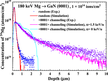
Fig. 1. (Color online) Depth profiles of 180 keV Mg implanted into GaN (0001) under channeled and random implantation conditions. The blue and purple dots show the experimental depth profiles obtained by SIMS in the case of random and channeled implantation conditions, respectively. The red line shows the simulated depth profile for random implantation. The pink and light blue lines show the simulated depth profiles for channeled ion simulations with different values of the parameters (α) involved in limiting the electronic stopping power.
Download figure:
Standard image High-resolution imageIn this calculation, the electronic energy loss was 1.2 times the Ziegler's value to reproduce the experimental value for random implantation shown in blue dots in Fig. 1. The Ga and N atoms in the GaN crystal were assigned 1-D thermal vibration amplitudes of 0.059 and 0.063 A, respectively. These values were averaged over the thermal vibration amplitudes calculated by Schowalter et al. 34) based on the experimental Debye–Waller factor results from X-ray diffraction by Xiong and Moss. 35) In this paper, 1.5 keV/u was used for α in both random and channeling simulations, and a value of 0.3 was used for the β coefficient. The simulation was performed assuming that the angular spread of the incident beam had a Gaussian distribution with a standard deviation of 0.7°. Figure 1 shows that the experimental Mg distributions of random and channeled implantations were well reproduced by the above parameters.
Figure 2 shows the depth profile of Mg concentration after channeled implantation of Mg with energies ranging from 50 to 180 keV. The open markers are SIMS analysis results, whereas the solid lines are simulation results. The parameters used in the simulation are the same as those for 180 keV except for the beam divergence angle, which was 1.3°, 1.0°, and 0.8° for 50, 80, and 120 keV, respectively. The simulated values reproduce the experimental values well for a wide range of energies.
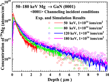
Fig. 2. (Color online) SIMS results (open markers) and simulation results (solid lines) for Mg distribution in GaN (0001) samples implanted with Mg ions with energies of 50–180 keV along the 〈0001〉 channeling axis.
Download figure:
Standard image High-resolution imageNext, we investigated the dose dependence of the Mg depth profile for an incident energy of 180 keV. Figure 3 shows the experimental and simulation results for doses differing by an order of magnitude. The increase in the peak Mg concentration was >20 times larger at the higher dose, whereas the increase at deeper levels was <10 times larger. These results suggest that at high doses, ion trajectories in the channeled condition were disturbed by defects produced during implantation. This effect was well reproduced by the simulation.
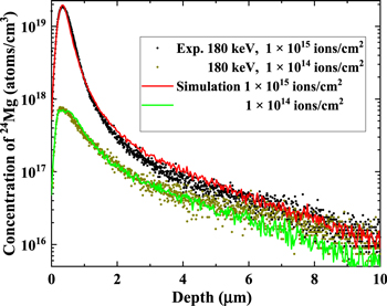
Fig. 3. (Color online) Depth profile of Mg implanted with 180 keV. The gray and black dots show the SIMS profiles for samples implanted with 1 × 10¹⁴ and 1 × 10¹⁵ ions cm−2, respectively. The green and red lines show the simulated depth profiles.
Download figure:
Standard image High-resolution imageTo quantitatively evaluate crystal defects during implantation, the percentage of Ga atoms displaced from their lattice positions was estimated by channeling Rutherford backscattering spectroscopy (RBS/C) analysis. Figure 4 shows the RBS/C spectra of the samples shown in Fig. 3 and an un-implanted sample. The green dots represent the random spectrum. In contrast, the orange, light blue, and blue dots show the channeling spectra of the un-implanted sample and of samples implanted with 1 × 10¹⁴ and 1 × 10¹⁵ ions cm−2, respectively. The red line is the result of fitting the channeling spectrum of the sample implanted with 1 × 10¹⁵ ions cm−2 using the RBS/C analysis tool. 36) The depth at maximum concentration estimated from Fig. 3 is approximately 0.25 μm. The ratio of the channeling yield of 1 × 10¹⁵ ions cm−2 to the random yield at that depth in Fig. 4 is approximately 4.9% (35/720 = 0.049). Since the yield fraction of the un-implanted spectrum is approximately 1.5% (11/720 = 0.015), it can be estimated that the ion implantation of 1 × 10¹⁵ ions cm−2 produced 3%–4% of the total disorder of Ga atoms at a depth of 0.25 μm.
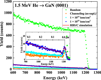
Fig. 4. (Color online) Channeling Rutherford backscattering spectroscopy (RBS/C) spectra of samples before and after ion implantation. The inset shows an enlarged view near the surface. The green and orange dots show the random and channeling spectra, respectively, prior to implantation. The light blue and blue dots show the RBS/C spectra of the samples after implantation with 1 × 10¹⁴ and 1 × 10¹⁵ ions cm−2, respectively, of 180 keV Mg under channeled implantation conditions. The red line shows the result of fitting analysis for the RBS/C spectrum. The scale in the inset shows the corresponding depth.
Download figure:
Standard image High-resolution imageThe Kinchin–Pease model, which uses the displacement energy (Ed) of atoms, and the NRT model, which is a modification of the Kinchin–Pease model, are often used to calculate the numbers of crystal defects created during implantation.
37,38) In scatGUI, the number of defects was calculated using the following equation with a correction factor (kNRT) added to the NRT model: defect count  where T is the recoil energy due to elastic scattering in a two-body collision. Ed values were calculated by Xiao et al. using first-principles calculations,
39) with defect calculations using 73.2 and 32.4 eV for Ga and N, respectively. In the calculations for each element, the energy T is distributed according to the compositional ratio, since recoil particles form a cascade of defects almost randomly. Defect generation and subsequent defect accumulation were calculated as follows. In the first trajectories simulation, the depth profile of the number of defects was obtained according to the above equation. In the second and subsequent simulations, it was assumed that some of the target atoms could exhibit large displacements (Gaussian distribution with standard deviation of 1 Å) in a Monte Carlo manner according to the simulated depth profile of the defects.
where T is the recoil energy due to elastic scattering in a two-body collision. Ed values were calculated by Xiao et al. using first-principles calculations,
39) with defect calculations using 73.2 and 32.4 eV for Ga and N, respectively. In the calculations for each element, the energy T is distributed according to the compositional ratio, since recoil particles form a cascade of defects almost randomly. Defect generation and subsequent defect accumulation were calculated as follows. In the first trajectories simulation, the depth profile of the number of defects was obtained according to the above equation. In the second and subsequent simulations, it was assumed that some of the target atoms could exhibit large displacements (Gaussian distribution with standard deviation of 1 Å) in a Monte Carlo manner according to the simulated depth profile of the defects.
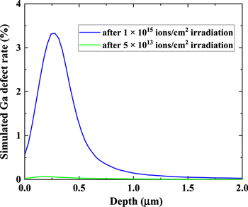
Figure 5 shows the depth profile of the calculated Ga defects. In the case of the 1 × 10¹⁵ ions cm−2, 20 calculations of 5 × 10¹³ ions cm−2 were performed to evaluate the defect accumulation. The number of defects (3%–4%) obtained by RBS/C analysis was reproduced assuming a kNRT value of 0.4 for Ga and N, respectively. The simulated depth distributions of Ga defects in the cases of samples implanted with 5 × 10¹³ and 1 × 10¹⁵ ions cm−2 are shown by the green and blue lines, respectively. The implantation profile calculation was also performed using a value of kNRT = 0.4, and the results reproduced the experimental values extremely well, as shown by the red line in Fig. 3.
Fig. 5. (Color online) Depth profile of Ga defects calculated with a defect formation correction factor of kNRT = 0.4. The green and blue lines show the calculated results after implantation with 5 × 10¹³ and 1 × 10¹⁵ ions cm−2, respectively.
Download figure:
Standard image High-resolution image
In summary, we demonstrated the advantages of implanting Mg ions into GaN under 〈0001〉 channeling conditions and developed simulation code (scatGUI) for this purpose. We showed the distributions of ion-implanted Mg across a range of doses and showed that the simulation can reproduce the Mg distributions by assuming defects during implantation in the high-concentration region. Channeling ion implantation is expected to be an essential process technology for GaN power devices. We believe that this code will facilitate the creation of devices using GaN in the future.
Acknowledgments
This work was partly supported by the Ministry of Education, Culture, Sports, Science and Technology (MEXT) "Program for research and development of next-generation semiconductor to realize energy-saving society" (Grant No. JPJ005357). The authors would like to thank Professor T. Mishima for valuable discussions and Enago for English language review.