

Abstract
We propose a novel method to generate p-type conduction and low resistivity in wide- and ultrawide-bandgap III-nitride semiconductors via doping of a magnetic element. This method is based on the energetic competition between the covalency of the magnetic element and the ligand nitrogen atoms and the exchange-correlation energy of the magnetic impurity. Using magnetic elements with large exchange-correlation energy, we can obtain p-type wide- and ultrawide-bandgap semiconductors, which are basically difficult to synthesize due to the unipolarity.
Export citation and abstract BibTeX RIS
Recently, much attention has been devoted to gallium nitride and aluminum nitride semiconductors for their potential application in high-power electronics. Wide- and ultrawide-bandgap semiconductors such as GaN and AlN exhibit high breakdown voltage, high saturation drift velocity, and high thermal conductivity; the bandgaps of GaN and AlN in wurtzite structure are 3.51 eV and 6.25 eV, respectively. 1) However, wide- and ultrawide-bandgap nitride semiconductors like GaN and AlN rarely show low-resistance p-type properties due to their unipolarity, charge compensation effect, and deep acceptor levels. By contrast, these materials tend to become n-type semiconductors when using the existing crystal growth methods. This presents an obstacle for their implementation in industrial applications.
The first p-type GaN samples were grown by Akasaki et al. 2) In these samples, p-type conduction was realized by doping GaN with Mg using a low-energy electron-beam irradiation treatment after crystal growth. Nakamura et al. found that GaN samples become n-type semiconductors, as Mg acceptors are compensated by H donors. 3) The low carrier concentration in these materials is due to the deep Mg acceptor level and H compensation, which are caused by the small permittivity of wide-bandgap semiconductors. Nakamura et al. obtained GaN with p-type semiconducting properties through the removal of H donors via heat annealing. 3) Moreover, Akasaki et al. fabricated blue LEDs using InGaN, 4) and blue and green laser devices were fabricated using low-resistance p-type InGaN. 5) In the 2000s, Nishikawa et al. succeeded in fabricating red LEDs using Eu-doped GaN. 6) This report made us expect the realization of monolithic fullcolor LEDs. These Eu-doped GaN LEDs were realized by introducing an n-type Eu-doped GaN layer between n-type and p-type GaN layers. This means probably that p-type Eu-doped GaN fabrication is basically difficult. O'donnell et al. reported that the p-n junction in Eu-doped GaN is made by GaN:Eu and GaN:Eu, Mg samples, where the p-type sample is also fabricated following the procedures of Akasaki's and Nakamura's groups. 7,8)
Yamamoto et al. proposed another codoping method for valence-electron control, which is simultaneous doping of n- and p-type dopants in thermal nonequilibrium conditions via molecular beam epitaxy. 9–11) The difficulty in the fabrication of low-resistance p-type wide-bandgap semiconductors is caused by the charge compensation effect due to the low solubility and low carrier activity, which are a consequence of the deep acceptor levels. If excessive pairs of acceptor and donor are introduced into semiconductors under inhomogeneous conditions, band modulations occur due to spinodal nano-decomposition. As a result, the activation energy of the deep acceptors decreases regardless of the band modulations, and then the carrier activity increases. The codoping method proposed by Yamamoto et al. has been successfully employed to obtain valence-electron control in wide-bandgap semiconductors. 10,12)
In this letter, we propose a novel method to generate p-type conduction in wide- and ultrawide-bandgap semiconductors via doping with a magnetic element. This novel method may be higher efficiency in fabricating magnetic semiconductors, because extra dopants are not necessary. It is based on an interpretation that the exchange-correlation energy of the magnetic impurity can be expressed as a function of the electron configuration. When a magnetic atom is replaced with a host cation, the magnetic atom is apt to take the same valence configuration as the host cation due to the covalency. Simultaneously, it prefers to take the half-filled configuration due to the exchange-correlation energy, because the exchange splitting and the exchange-correlation energy are the largest when the electron configuration is the half-filled configuration. This situation causes energetic competition between the covalency and the exchange-correlation energy. As a result, the magnetic atom forms a hybridized state with the ligand anion, and then the electron occupation is modulated via the charge compensation effect. If a magnetic impurity with the half-filled configuration is doped into a III–V semiconductor, this electron occupation modulation appears as a charge transfer from the host anion to the magnetic impurity atom. As a result, holes are introduced into the valence band maximum, resulting in p-type conductance. Since this conductive state is generated in the state of the host anion, the resistivity should be lowered. We may call method as exchange-correlation-induced doping (EX-doping) method, because this method is based on stability due to the exchange-correlation energy.
We employed the MACHIKANEYAMA program package developed by Akai, where the Korringa–Kohn–Rostoker (KKR) Green's function method within the density functional theory is implemented. 13–15) The variational pseudo self-interaction correction (VP-SIC) method is used for the exchange-correlation potential as well as the Moruzzi–Janak–Williams potential. 16) The local density approximation is not applicable for 4f rare earth compounds, whereas the VP-SIC correction is useful for these systems. The relativistic effects were treated with the scalar relativistic approximation. The k-sampling points were 1034 and 440 for Eu-doped GaN/AlN and Mn-/Mn, O-doped GaN, respectively. The spin–orbit coupling is included within the spin diagonal terms. Experimentally measured lattice constants of the host nitride were used for the present calculations. Here, the metastable zincblende structures for AlN and GaN were considered, as low carrier scattering, high thermal conductivity, and high stiffness are expected for structures with a higher degree of lattice symmetry. 17,18) The present calculations are considered for impurities via the coherent potential approximation (CPA). 19) CPA, in which the multiple scattering effect is replaced with that of an effective-medium potential, treats the randomness of the doped impurities in the host semiconductors self-consistently; therefore, the supercell method was not necessary in these calculations.
First, a rare-earth-doped case is discussed. Figures 1(a) and 1(b) show the partial DOSs projected onto the magnetic impurity, Eu, and the host elements, Ga and N, in Eu-doped zincblende GaN, respectively. In this system, Eu atoms with a concentration of 8% were introduced. The Eu-4f state shows a large exchange splitting, which is about 11 eV. The Eu-4f state is split into bonding and antibonding states via the strong p–f hybridization between Eu-4f and N-2p, where the weak peak corresponding to Eu-4f antibonding states appears at the Fermi level and the strong peak corresponding to Eu-4f bonding states appears at −2.5 eV. The Eu-4f optical intra-transition of Eu-doped GaN (red light emission) is related to the transition between these two states splitted by the ligand field, where the Eu red light emission based on the 4f intra-transition is 2.2 eV. 8)

Fig. 1. (Color online) Electronic structure of Eu-doped zincblende GaN. Calculated partial DOS projected onto (a) Eu atoms and (b) to Ga and N atoms.
Download figure:
Standard image High-resolution imageIn general, Eu takes divalent or trivalent states in most practical situations. However, the present Eu partial DOS includes 0.5 holes, as shown in Table I. As mentioned earlier, this electronic structure is caused by the energetic competition between the strong covalency of this wide-bandgap semiconductor and the large exchange-correlation energy of the rare earth element. The competition causes the strong hybridization between N-2p and Eu-4f. This hybridization gives rise to the bonding state in the majority-spin state in the deep energy region and it pushes up the antibonding state up to the valence band maximum. This transformation proves to be energetically more favorable than the electronic structure modulation of the ligand field, rendering the system stable. Eventually, 0.5 holes are transferred to the valence band maximum due to charge neutrality. These holes give rise to p-type conductance. Because holes are composed of delocalized N-2p states, the resistivity should be low. By contrast, holes with the Eu-4f character little contribute to the conduction because they are strongly localized and also the concentration of Eu is too low.
Table I. Occupation, electrons, holes, and magnetic moments in nitride. These values were calculated using the Muffin-Tin spheres of Eu and Mn in the KKR method.
| Material | Occupation in the majority-spin band | Occupation in the minority-spin band | Electrons | Holes | Magnetic moment |
|---|---|---|---|---|---|
| (μB ) | |||||
| GaN:Eu | 6.44 (f) | 0.06 (f) | 6.50 (f) | 0.50 | 6.38 (f) |
| 2.45 (p) | 2.39 (p) | 4.84 (p) | 0.06 (p) | ||
| 0.03 (s) | 0.04 (s) | 0.07 (s) | −0.01 (s) | ||
| AlN:Eu | 6.46 (f) | 0.08 (f) | 6.54 (f) | 0.46 | 6.38 (f) |
| 2.29 (p) | 2.21 (p) | 2.50 (p) | 0.08 (p) | ||
| 0.04 (s) | 0.05 (s) | 0.09 (s) | −0.01 (s) | ||
| GaN:Mn | 4.08 (d) | 0.34 (d) | 4.42 (d) | 0.58 | 3.74 (d) |
| 0.08 (p) | 0.07 (p) | 0.15 (p) | 0.01 (p) | ||
| 0.06 (s) | 0.05 (s) | 0.09 (s) | 0.01 (s) | ||
| GaN:Mn, O | 4.19 (d) | 0.27 (d) | 4.46 (d) | 0.54 | 3.82 (d) |
| (O = 3%) | 0.08 (p) | 0.07 (p) | 0.15 (p) | 0.01 (p) | |
| 0.06 (s) | 0.05 (s) | 0.11 (s) | 0.01 (s) | ||
| GaN:Mn, O | 4.26 (d) | 0.24 (d) | 4.50 (d) | 0.50 | 4.02 (d) |
| (O = 5%) | 0.08 (p) | 0.07 (p) | 0.15 (p) | 0.01 (p) | |
| 0.06 (s) | 0.05 (s) | 0.11 (s) | 0.01 (s) |
The electronic structure in this system facilitates the extension of the magnetic percolation path. Accordingly, the ferromagnetic state is dominant in this system. 20) In fact, room temperature ferromagnetism of Eu-doped GaN and the large magnetic moment per Gd ion in Gd-doped GaN were observed, and this mechanism successfully demonstrated based on the related interpretation: the magnetic percolation path is generated by the N-2p holes that are introduced upon doping with Eu, which exhibit an atomic radius larger than that of Ga (e.g. the volume compensation effect). 21,22)
In the second example, an ultrawide-bandgap semiconductor (AlN) is discussed. The bandgap of AlN is 6.4 eV. Figure 2 shows the DOS of AlN doped with Eu with an 8% concentration. In Fig. 2(a), the black solid lines indicate the total DOS, whereas the red dashed lines indicate the DOS projected onto the Eu atoms, the blue and green dashed lines indicate the DOS projected onto the N and Ga atoms, respectively. The electronic structure of this system is similar to that of the previous system. In this system, the strong p–f hybridization causes the Eu-4f state in the majority-spin states moving energetically downward, becoming a bonding character, and pushes the N-2p state up to the valence band maximum, becoming an antibonding state. As a result of electron redistribution into Eu-4f from N-2p, 0.5 s or p holes are introduced into the valence band maximum, and eventually, low-resistance p-type semiconductors are realized. However, the energy difference between the bonding and the antibonding states are smaller than that of Eu-doped GaN. This is because the covalency of AlN is stronger than that of GaN.
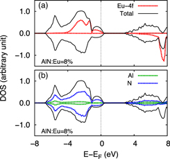
Fig. 2. (Color online) Electronic structure of 8%-Eu-doped zincblende AlN. Calculated partial DOS projected onto (a) Eu atoms and (b) to Al and N atoms.
Download figure:
Standard image High-resolution imageIn the third example, a 3d-transition-metal-doping case is discussed. Figure 3 shows the electronic structure of GaN doped with Mn with a 5% concentration. The arrow in this figure indicates the primary peak of the Mn 3d bonding states that are observed in photoemission experiments. 23) Mn occupies the Ga sites exhibiting an electronic configuration between d4 and d5, and a single hole (= 0.6 3d holes + 0.4 N-2p holes) occupies the antibonding impurity band. This situation is similar to the Eu-doped GaN and Eu-doped AlN cases. That is, in this system, the holes that occupy partially the antibonding impurity band cause a decrease in the band energy, resulting in p-type conductance. This simultaneously makes the double-exchange interaction dominant, which renders the ferromagnetic state stable. 24) Since N ions provide conduction path over the whole crystal, the low resistivity is expected. This result is consistent with the report by Sonoda et al.; Mn-doped GaN films show p-type conductivity. 25)

Fig. 3. (Color online) Electronic structure of 5%-Mn-doped zincblende GaN. Calculated partial DOS projected onto (a) Mn atoms and onto (b) Ga and N atoms. The arrow indicates the primary peak of Mn 3d states observed in photoemission experiments. 23)
Download figure:
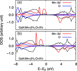
Standard image High-resolution imageFinally, the case of electron doping in Mn-doped GaN is discussed. Figure 4 shows the DOS of (Mn, O)-codoped GaN, where the concentration of Mn is fixed to 5%. The concentration of O is 3% in Fig. 3(a) and 5% in Fig. 3(b). In these figures, the black solid lines indicate the total DOS, the red dashed lines indicate the Mn 3d states, and the blue dashed lines indicate the O states. O is a donor in this situation; hence, it provides electrons to the crystal. The provided electrons increase the exchange-correlation energy of the Mn 3d states, because it makes the electron configuration approach the half-filled configuration. This can be confirmed by comparison between undoped case shown in Fig. 3(a) and 3%-O-doped case shown in Fig. 4(a). The electron-doped exchange splitting shown in Fig. 4(a) is larger than the undoped exchange splitting shown in Fig. 3(a). This oxygen-induced exchange splitting enhancement is further increased upon increasing of the oxygen concentration. In the case of 5% O, the primary peak of the Mn 3d states, which is indicated by the photoemission experiments, shifts energetically downward. When the Mn 3d states become the half-filled configuration, i.e. d5, the energy gain is the largest. Therefore, such electron doping may control resistivity of this p-type conduction. Note that this result cannot be described within the rigid-band model.
Fig. 4. (Color online) Electronic structure of zincblende GaN codoped with Mn and O. The concentration of Mn and O are (a) 5% and 3%, respectively, and (b) 5% and 5%, respectively.
Download figure:
Standard image High-resolution image
In summary, a method to generate p-type conduction in wide- and ultrawide-bandgap III-nitride semiconductors via doping of a magnetic element is proposed in this letter. This novel method is based on energetic competition between the covalency of the magnetic impurity and the ligand nitrogen and the exchange-correlation energy of the magnetic impurity. When a magnetic atom is replaced with a host cation, the former, on one hand, is apt to take the same valence configuration as the host cation due to the covalency but, on the other hand, it also prefer to simultaneously take the half-filled configuration due to the existence of exchange-correlation energy. If the system does not have sufficient number of electrons to satisfy the both conditions, holes are introduced into the valence band maximum, resulting in p-type conduction. Since this conduction is contributed by the state belonging to the host anion, the resistivity should be low.
Acknowledgments
This work was partly supported by JST CREST (Grant Nos. JPMJCR1777 and JPMJCR18I2) and JPSJ KAKENHI (Grant Nos. 18K04926 and 18H05212). This work was partly supported by Osaka University International Joint Research Promotion Program (B). Computations were done at the Supercomputer Center, ISSP, University of Tokyo. This work was also partly supported by MEXT as "Program for Promoting Researches on the Supercomputer Fugaku" (DPMSD) and used computational resources of supercomputer Fugaku provided by the RIKEN Center for Computational Science through the HPCI System Research Project (Project ID: hp210179).