

Abstract
Metal-oxide-semiconductor capacitors with HfO2/1-monolayer TiO2/SiO2 stacks were examined to explore the origin of the interface dipole modulation. The capacitance–voltage (C–V) measurements exhibited that the polarity of the interface dipole layer changes depending on the gate bias. The hard X-ray photoelectron spectroscopy measurements demonstrated that an applied gate voltage induces small changes in the Ti–O chemical bonding and potential profile around the HfO2/SiO2 interface.
Export citation and abstract BibTeX RIS

Content from this work may be used under the terms of the Creative Commons Attribution 4.0 license. Any further distribution of this work must maintain attribution to the author(s) and the title of the work, journal citation and DOI.
The material HfO2 is used as a gate dielectric layer in a current type of advanced MOS field-effect transistors (FETs), and it has a high material affinity with semiconductor device technology. 1–3) There are many studies on emerging HfO2-based memory devices, such as a resistance-change random-access memory using oxygen vacancies in the HfO2 and a ferroelectric FET (FeFET) with a thin ferroelectric HfO2 layer. 2,4–8) One advantage of these devices is the capability to fabricate high-density memory devices via the current semiconductor manufacturing platform. In particular, the technical hurdles of HfO2-based FeFETs are expected to be low, as it has essentially the same device structure as the current MOS FETs. The key issue is the precise control of the ferroelectric crystal phase, which involves the annealing procedure, the selection of dopant atoms, and the dopant concentration. 7–11) On the other hand, an amorphous-HfO2-based MOS memory device, which can be fabricated by a low-temperature process, was recently proposed. 12,13) Amorphous HfO2/SiO2 MOS capacitors with an atomically thin interfacial TiO2 layer have been reported to exhibit C–V hysteresis similar to that of ferroelectric MOS capacitors. The hysteresis width induced by a single HfO2/SiO2 stack is too small (∼0.3 V) to be sufficient for memory applications, so a multi-stack HfO2/1-ML TiO2/SiO2 structure has been proposed. 12,14,15) As for the mechanism of these C–V characteristics, an interface dipole modulation (IDM) induced by Ti–O bond breakage/repair or bonding configuration change has been proposed. 12,14) However, there have been few reports on IDM mechanism, and our understanding of it is not sufficient. In this study, we examine single HfO2/1-ML TiO2/SiO2 MOS stacks, which are the simplest IDM structures, by using the C–V and HAXPES methods.
First, a 10 nm thick SiO2 layer was formed on an n-type Si(100) substrate by a thermal oxidation method. Second, by immersing the substrate in a diluted HF solution, the SiO2 layer was etched and thinned to about 7 nm. Third, the sample was introduced into an ultra-high vacuum chamber and heated at above 350 °C for longer than 10 min to desorb the adsorbed molecules of species such as water. After cooling down to room temperature, 1-ML TiO2 and HfO2 layers were deposited by an EB evaporation method. 12–14) To provide a sample for C–V measurements, an HfO2 layer with a thickness of 2–7 nm was deposited on the same substrate by gradually moving a shutter between the EB evaporator and the substrate. Finally, the post-deposition annealing was performed at 350 °C for 30 min, and 50 nm thick Al was then deposited as a gate electrode by using a stencil mask. To provide a HAXPES sample, 1-ML TiO2 and 2 nm thick HfO2 layers were also deposited on a 10 nm thick SiO2/n-Si substrate. Because the gate electrode has to be thin enough to enable detection of photoelectrons emitted from the oxide stack underneath, 16,17) a 15 nm thick Ir layer was deposited on the HfO2. The HAXPES measurements were performed with synchrotron radiation (hν = 7940 eV) in the BL47XU at SPring-8. 18,19)
As seen in Fig. 1(a), a transmission electron microscopy (TEM) image of the prepared MOS stack showed that the HfO2 and SiO2 were amorphous and the reaction at their interface was negligible. Note that the TEM contrasts of TiO2 and SiO2 are at the same level. The high-frequency C–V curve shown in blue in Fig. 1(b) indicates a counterclockwise hysteresis, which is the same as the IDM operation reported in previous papers. 12–15) Those studies used Ir and Au, which are metals with a large work function (ΦM > 5 eV), as the gate electrode. The present C–V data is the first demonstration with Al, a metal with a low work function (ΦM ∼ 4.25 eV). In high-frequency C–V measurements for an n-type Si substrate, it is well known that a sufficient oxide electric field in the negative bias range is not produced because of the formation of a depletion layer. 20) The red curves in Fig. 1(b) show the C–V hysteresis measured at 5 kHz under laser-light illumination (730 nm) in which the sufficient minority carriers were supplied to overcome the above issue. 12,13) A C–V shift starting from the initial curve was found towards both the positive and negative biases. Here, the flat-band voltage, Vfb, was estimated; it is shown by the dotted green curves in Fig. 1(b), and its bias dependence is plotted in Fig. 1(c). There was a saturation tendency at a bias range wider than ±4 V, and estimated maximum hysteresis width is about 0.3 V.

Fig. 1. (Color online) C–V measurements of HfO2/1-ML TiO2/SiO2 MOS capacitors. (a) TEM image of a typical MOS capacitor. Position of 1-ML TiO2 layer is indicated by green arrow. (b) C–V hysteresis curves measured under high-frequency and light-illuminated conditions. (c) Gate-voltage-induced Vfb shifts estimated by light-illuminated C–V method. (d) Maximum and minimum Vfb values measured for MOS capacitors with various HfO2 thicknesses.
Download figure:
Standard image High-resolution imageThe oxide thickness dependence is well known to provide information about the electric charge position in a MOS stack,
20–22) so we examined the effect of the HfO2 thickness on the switched Vfb, i.e. the maximum and minimum Vfb values, as shown in Fig. 1(d). The HfO2 thickness [ (nm)] was estimated from the equivalent oxide thickness determined from the high-frequency C–V measurements.
22–24) In the following discussion, we assume that two types of electric charges at the HfO2/1ML-TiO2/SiO2 interfaces were changed by the gate voltage: a unipolar sheet charge [qSI
(cm−2)] and a dipole layer with positive and negative changes, respectively, on the HfO2 and SiO2 sides [Φdipole (V)]. This means that the electric charges near the electrode/HfO2 and the SiO2/Si interfaces are ignored. The Vfb value can be expressed by the following equation:
20–22)
(nm)] was estimated from the equivalent oxide thickness determined from the high-frequency C–V measurements.
22–24) In the following discussion, we assume that two types of electric charges at the HfO2/1ML-TiO2/SiO2 interfaces were changed by the gate voltage: a unipolar sheet charge [qSI
(cm−2)] and a dipole layer with positive and negative changes, respectively, on the HfO2 and SiO2 sides [Φdipole (V)]. This means that the electric charges near the electrode/HfO2 and the SiO2/Si interfaces are ignored. The Vfb value can be expressed by the following equation:
20–22)

where, ΦMS (V) is the work function difference between Si and the Al gate metal, and  is the dielectric constant of the HfO2 layer with the relative dielectric constant of approximately 20.
23,24) Ignoring the interface dipole, the switching between the positive sheet charge (4.1 × 1012 cm−2) and the negative sheet charge (3.2 × 1012 cm−2) produced the dotted lines shown in Fig. 1(d). This calculated tendency is different from the experimental data. In contrast, the solid lines in Fig. 1(d) were calculated by considering both types of charges, and this result is suitable for explaining the experimental data. In this case, the sheet charge density, SI
, was estimated to be low (<3 × 1011 cm−2) and the interface dipole, Φdipole, switched between –0.14 and +0.18 V. This indicates that the polarity reversal of the interface dipole was the main contribution to the observed hysteresis characteristics.
is the dielectric constant of the HfO2 layer with the relative dielectric constant of approximately 20.
23,24) Ignoring the interface dipole, the switching between the positive sheet charge (4.1 × 1012 cm−2) and the negative sheet charge (3.2 × 1012 cm−2) produced the dotted lines shown in Fig. 1(d). This calculated tendency is different from the experimental data. In contrast, the solid lines in Fig. 1(d) were calculated by considering both types of charges, and this result is suitable for explaining the experimental data. In this case, the sheet charge density, SI
, was estimated to be low (<3 × 1011 cm−2) and the interface dipole, Φdipole, switched between –0.14 and +0.18 V. This indicates that the polarity reversal of the interface dipole was the main contribution to the observed hysteresis characteristics.
A similar analysis was reported for IDM MOS capacitors with Ir gate electrodes, 13,14) and those results have been proposed to provide one reasons for the IDM mechanism. However, the maximum and minimum Vfb for the Ir-electrode samples were always smaller than the ideal Vfb, so the strength of the interface dipole was considered to have changed. This is different from the dipole polarity reversal of the present Al-electrode samples. We consider that this difference is related to the charge distribution around the metal/HfO2 interface. From Al/HfO2/SiO2/Si MOS capacitors without interface Ti oxide, Φdipole was estimated to be about 0.02 V, which was almost consistent with that estimated for Al/SiO2/Si MOS capacitors. This means that the dipole at the Al/HfO2 interface is negligibly small. On the other hand, Φdipole of Ir/HfO2/SiO2 stacks was reported to be larger than 0.2 V. 13,22) This dipole is probably present at the Ir/HfO2 interface rather than at the HfO2/SiO2 interface. In fact, several groups have proposed dipole formation at the contact between HfO2 and a metal with a large work function. 25,26) Therefore, we concluded that the initial dipole at the HfO2/SiO2 interface is small in both electrode samples, and in the IDM operation, interface dipoles with opposite polarities are formed depending on the induced electric field direction.
In the HAXPES measurements, the gate electrode was connected to the ground and a voltage was applied to the Si back contact, as illustrated in Fig. 2(a). For convenience of comparison with the above C–V measurements, the substrate voltage is denoted as –Vg (V) in the following explanation. The curves indicated (I) in Fig. 2(b) are the Hf 3d, Si 1s, and Ti 1s photoelectron spectra observed before applying the voltage. These curves show that the HfO2, SiO2, and TiO2 were major components and each suboxide was small. 16,27–30) This result is consistent with previous standard X-ray photoelectron spectroscopy results for the HfO2/1-ML TiO2/SiO2 structure without an electrode. 13) Thus, we conclude that the formation of the Ir electrodes does not induce defects in the oxide stack.
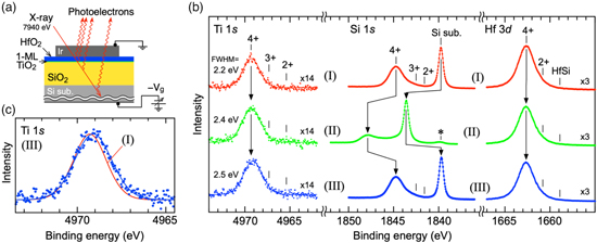
Fig. 2. (Color online) HAXPES measurements of a HfO2/1-ML TiO2/SiO2 MOS capacitor. (a) Schematic illustration of the MOS sample measurement. (b) Hf 3d, Si 1s, and Ti 1s photoelectron spectra measured under the gate voltage conditions of (I) Vg = 0 V, (II) Vg = –5 V, and (III) Vg = 0 V after Vg = –5 V. (c) Ti 1s photoelectron spectra of (III), and fitting curves of (I) and (III).
Download figure:
Standard image High-resolution imageThe curves indicated by (II) in Fig. 2(b) show that an applied voltage of Vg = –5.0 V caused a large binding energy shift and spectral change in the Si 1s photoelectron spectrum, but the Hf 3d and Ti 1s spectra were only slightly changed. This behavior can be mostly explained via the change in the band diagrams shown in Fig. 3. The peak shift of the Si substrate reached about 4 eV, suggesting that about 4 V was applied to the HfO2/1-ML TiO2/SiO2 stack structure. This is reasonable given the Si surface band bending and the parasitic series capacitance. The spectral shape for the oxide components at Vg = –5.0 V is obviously different from the spectral shape at Vg = 0 V. This can be explained by the inclined SiO2 band shown in Fig. 3(b). Even if the chemical composition is the same, the binding energy shifts according to the potential drop. The Si oxide spectrum is the integration of the photoelectrons emitted from such an inclined SiO2 band. 16) Therefore, we can conclude that the applied voltage caused the large spectral change, especially in the SiO2 layer. Note that a small peak indicated by "*" in Fig. 2(b) (II) remained at the binding energy of Si substrate. This is presumed to be due to stray photoelectrons from the area not covered by the Ir. On the other hand, the Hf 3d peak shift is as small as 0.1 eV. This is consistent with the band diagram in Fig. 3(b), where the band slope of the HfO2 layer with a high dielectric constant must be smaller than that of the SiO2 layer. The peak shift of Ti 1s is also small, which is consistent with the small potential drop of the interfacial Ti oxide as shown in Fig. 3(b).

Fig. 3. (Color online) Band diagrams for the HAXPES measurements of the HfO2/1-ML TiO2/SiO2 MOS capacitor. (a) Vg = 0 V conditions, and (b) negative Vg conditions.
Download figure:
Standard image High-resolution imageWhen the gate voltage was returned to Vg = 0 V, all the spectra returned to being almost the same as before applying the voltage. On the other hand, we can find a slight difference in the Ti 1s spectra, i.e. the full width at half maximum (FWHM) changes from 2.2 to 2.5 eV by applying –5 V. The spectral change shown in Fig. 2(c) could be related to the Ti–O bonding configuration (bond length and angle) and the formation of Ti2O3. A more elaborate measurement with higher resolution and higher sensitivity is required to identify the structural change. On the other hand, FWHM returned to 2.2 eV after applying voltage of +3 V (not shown). Therefore, we considered that the above Ti 1s spectral change is a reversible phenomenon similar to the IDM operation. In addition, the above speculation is consistent with the previously reported IDM mechanism with Ti–O structural change. 12,14)
Figure 4(a) shows the Si 1s (4+) and Hf 3d (4+) spectra at Vg = 0 V, which reveal that the peak binding energy difference, BESi1s–Hf4d = Si 1s (4+)-Hf 4d (4+), decreased slightly after applying a voltage of –5 V. The change in BESi1s–Hf4d, δBESi1s–Hf4d = BESi1s–Hf4d–BESi1s–Hf4d (initial), is plotted in Fig. 4(b). As indicated by the blue circles, large δBESi1s–Hf4d shifts took place naturally when the voltage was applied. The red rhombuses show the behavior for Vg = 0 V, zero-voltage δBESi1s–Hf4d, indicating that the δBESi1s–Hf4d decreased after applying voltage of –3 and –5 V. These changes can be explained by the change in the interface dipole, as shown in Fig. 3(a). Here, we assume an interface dipole with positive changes on the HfO2 side and negative changes on the SiO2 side. If this dipole polarity switches, δBESi1s–Hf4d is expected to become small. This behavior is also consistent with the above C–V characteristics, i.e. the C–V curve is shifted toward a positive bias by applying a negative voltage. On the other hand, δBESi1s–Hf4d decreased by about 0.2 eV after applying a voltage of –5 V, which is slightly smaller than the maximum C–V hysteresis mentioned above. This difference can be explained by the band diagram in Fig. 3(a). Even at Vg = 0 V, the energy bands of the SiO2 and HfO2 layers are expected to be slightly tilted. The Si 1s (4+) and Hf 4d spectra are the integration of photoelectrons emitting from these SiO2 and HfO2 layers, respectively. The spectral peak position can be roughly estimated to be the photoelectron binding energy at the center of the oxide layer. Therefore, it is reasonable that the peak energy difference is smaller than the potential change at the SiO2/HfO2 interface. From the above results, we conclude that the same phenomenon was detected in both the C–V and HAXPES measurements. On the other hand, the interface dipole was already formed before applying the voltage in the HAXPES measurement. We consider that the interface dipole has already been produced by the X-ray irradiation.

Fig. 4. (Color online) Effect of the applied voltage Vg on the binding energy difference between the Si 1s (4+) and Hf 3d (4+) photoelectron peaks (BESi1s–Hf3d). (a) Si 1s and Hf 3d photoelectron spectra before and after applying a voltage of –5 V. (b) Difference from initial BESi1s–Hf3d, δBESi1s–Hf3d = BESi1s–Hf3d–BESi1s–Hf3d (initial). The blue circles show the voltage dependence. The red rhombuses show zero-voltage δBESi1s–Hf3d, which shows the changes induced by applying the voltage.
Download figure:
Standard image High-resolution image
Finally, we discuss the other mechanisms that could produce the above counterclockwise C–V hysteresis: (1) mobile electric charges in the oxide stack, and (2) carrier transfer between the gate electrode and the carrier traps in the oxide stack. We first consider the defect-related mobile charges or carrier traps around the interfacial Ti atoms. In this case, Vfb must be proportional to the HfO2 thickness, as expected from Eq. (1). Our experimental data rejects this scenario. If mobile charges or carrier traps are formed in the HfO2 near the electrode, the measured Vfb shifts can be explained. In this case, a usual HfO2/SiO2 MOS stack without an interfacial TiO2 layer should have a similar C–V hysteresis. In addition, if the metal/HfO2 contact induces such defects, the hysteresis characteristics are expected to depend on the electrode material. Furthermore, as seen in Fig. 4(a), the peak shift of Hf 3d is much smaller than that of Si 1s, suggesting that the change in the potential distribution of the HfO2 layer is small. Therefore, from the above C–V and HAXPES measurements, we conclude that the polarity of the interface dipole in the HfO2/1-ML TiO2/SiO2 structure is switched by applying the voltage. The structural change observed for the interfacial Ti oxide described above is considered to induce the polarity reversal of the interface dipole.
In conclusion, the C–V measurements of the HfO2/1-ML TiO2/SiO2 MOS stack revealed that polarity reversal of interface dipole produces the Vfb shift of about 0.3 V. The HAXPES measurement exhibited a small change in the Ti–O chemical bonding and supported the potential change between the HfO2 and SiO2 layers.
Acknowledgments
This work was supported by JSPS KAKENHI Grant Number 16H02335 and 19H02178. The experiments were partly performed at SPring-8 with the approval of the program review committee (2016B0109 and 2018A1360).