

Abstract
Active metasurfaces using metal–insulator transition materials such as vanadium dioxide (VO2) have been demonstrated recently. As most of them are based on plasmonic metasurfaces, it is difficult to realize transmissive devices at optical frequencies. In this study, we theoretically propose and demonstrate the transmission type of an active all-dielectric metasurface mediated by VO2. We numerically study the optical properties of a cylindrical Mie resonator consisting of crystalline silicon and VO2 layers, and we find that it achieves a 2π phase shift of approximately 1550 nm by tuning the radius. The proposed structure can be applied to non-mechanical beam steering, polarizers, metalenses, etc.
Export citation and abstract BibTeX RIS
There is considerable interest in metasurfaces owing to their use in various compact optical components. Metasurfaces are two-dimensional artificial media that can control the amplitude, phase, and polarization of reflected/transmitted light at a subwavelength scale. 1–4) The metasurface is extremely thin and it can be used to miniaturize conventional optical components. A significant research topic on metasurfaces is wavefront control with 2π phase coverage. By obtaining 2π phase coverage, we can fully control the wavefront of the reflected/transmitted light and apply it to beam steering, 5,6) holograms, 7,8) polarizers, 9,10) and flat lenses. 11,12) These applications play a crucial role in the miniaturization of photonic devices.
Recently, active metasurfaces using phase-change materials have attracted much interest. 13,14) Several studies have been conducted using phase-change materials such as indium tin oxide, 15–17) Ge2Sb2Te5, 18–21) and vanadium dioxide (VO2). 22–26) We have focused on VO2 considering it drastically changes the refractive index between the dielectric and metal on the order of picoseconds at relatively lower temperatures of 341 K and can be tuned using thermal, electrical, and optical methods. 27)
Although active metasurfaces utilizing VO2 have been reported, 22–26) various studies have been conducted on plasmonic metasurfaces based on metal–dielectric–metal structures that utilize surface plasmon polaritons. 28,29) Considering that plasmonic metasurfaces suffer from a significant loss during transmission, the efficient wavefront control of transmitted waves is difficult to realize. In fact, the transmission type of wavefront control has been reported only at 100 GHz. 22) All-dielectric metasurfaces (DMSs) composed of Mie resonators supporting various multipole modes have shown great potential in resolving the above problems for plasmonic metasurfaces. 30–36) Although several studies on active DMSs have been reported, it is still challenging to realize active operation at optical frequency by utilizing VO2. 22–26)
In this study, we propose a method for transmitted active phase control using DMS mediated by VO2 (DMSV). DMSV achieves a 2π phase coverage in the dielectric phase and a high contrast in the phase difference between the dielectric and metal phases at 1550 nm.
Figure 1(a) shows a schematic image of a meta-atom of DMSV: a cylindrical resonator on an Al2O3 substrate (refractive index of n = 1.7). The resonator is composed of VO2 and crystalline silicon (c-Si) (n = 3.5) layers with a radius of r. Here, the period of the resonator P is fixed at P = 750 nm and the thicknesses of c-Si (t1) and VO2 (t2) are 450 nm and 300 nm, respectively. The real and imaginary parts of the permittivity of VO2 are taken from our previous paper. 37) Note that Al2O3 substrate is selected for lattice matching to VO2 in epitaxial growth.

Fig. 1. (Color online) (a) A schematic image of a unit cell of DMSV composed of c-Si and VO2 cylindrical resonators on the Al2O3 substrate, (b) transmitted phase, and (c) transmittance of DMSV at 1550 nm versus radius from 50 nm–250 nm. The blue and red lines denote the dielectric and metal phase of VO2, respectively.
Download figure:
Standard image High-resolution imageTo investigate the optical properties of DMSV, we performed finite-difference time-domain (FDTD) simulations (Ansys Lumerical FDTD) to obtain transmission spectra and phase shifts in both the dielectric and metal phases of VO2 at 1550 nm. We used a light source with a y-polarized electric field.
Figures 1(b) and 1(c) show the transmittance and transmitted phase in the dielectric (blue line) and metal phase (red line) of the VO2 layer with r ranging from 50–250 nm, respectively. In the dielectric phase, we find that DMSV obtains 2π phase coverage by changing r while only 0.5π coverage in the metal phase. In the dielectric phase, a resonant dip structure is observed in the transmittance at r = 186 nm. Around the dip, the transmitted phase changed significantly. In the metal phase, a similar dip structure is observed in the transmittance at r = 198 nm. These effects are attributed to the change in the Mie resonant condition, as discussed below.
To clarify the mechanism, we consider an array of a uniform c-Si cylinder with fixed r = 186 and P = 750 nm as a simple model. Figures 2(a) and 2(b) show the transmittance and phase shift spectra in the near-infrared region for transmitted waves with heights t1 = 450 and 750 nm, respectively. As shown in Fig. 2(a), perfect reflections (i.e., transmission dips) caused by electric dipole (ED) and magnetic dipole (MD) resonances are observed at 1250 nm and 1500 nm, respectively [see supplementary data S1 (available online at stacks.iop.org/APEX/14/032007/mmedia)]. At the ED and MD resonances, steep phase shifts with almost π are observed. It is known that ED and MD resonances allow for a maximum π phase shift. 34) In contrast, a phase shift of 2π is observed at the dip around 1650 nm, as shown in Fig. 2(b). We attribute such a 2π phase shift to the degenerate effect of the ED and MD modes, which is observed in the calculated spectral map (see supplementary data S2). Namely, a 2π phase shift is caused by the Huygens' state. 34)
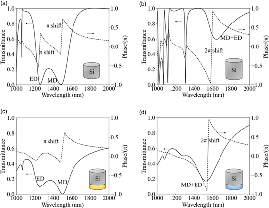
Fig. 2. (Color online) Transmittance (solid lines) and transmitted phase (dashed lines) of various cylindrical resonators with fixed P = 750 nm and r = 186 nm: c-Si resonators with (a) t1 = 450 nm, (b) t1 = 750 nm and t2 = 0 nm. c-Si/VO2 resonators (t1 = 450 nm, t2 = 300 nm) in the (c) metal and (d) dielectric phase of VO2.
Download figure:
Standard image High-resolution imageFigures 2(c) and 2(d) show the transmittance and phase shift spectra of DMSV with fixed r = 186 nm in the metal and dielectric phase of VO2, respectively. The transmittance in Fig. 2(d) is decreased compared to Fig. 2(b) due to the absorption in the VO2 layer caused by a lossy optical property in the dielectric phase. It is clearly observed that a 2π phase shift occurs only in the dielectric phase [Fig. 2(d)], although a π phase shift occurs in the metal phase [Fig. 2(c)]. In Fig. 2(c), the phase shift due to ED is weakened compared with the π shift observed in Fig. 2(a). Furthermore, the transmission dip due to ED is also weakened. Such effects are attributed to the mirror image effect (see supplementary data S3). Recently, some researchers have studied Mie resonators placed on a metal film. 38,39) The mirror image effect is a phenomenon whereby an object on a metal film is reflected and behaves as if it is located inside the metal film. The incident electric field is projected antiparallel while the incident magnetic field is projected parallel inside the metal film. Hence, considering the mirror image effect in a Mie resonator on a metal film, ED is completely cancelled out, resulting in a weakened phase shift as well as transmittance. We note that ED can be excited slightly due to insufficient cancelling by the finite range of a metal disk instead of an infinite metal film. Such a simple model suggests that the 2π phase shift observed in Fig. 1(c) is attributed to the volume change of the resonator. The resonator composed of c-Si and VO2 behaves as a single homogeneous dielectric medium, since the refractive index of c-Si and VO2 are approximately 3.5 and 3.2 at 1550 nm, respectively. As the volume of the high-index material is approximately identical to that in Fig. 2(b), the degenerate MD and ED modes are excited simultaneously, leading to 2π phase coverage. In addition, we note that the phase shift of π (≪2π) observed in Fig. 2(c) is qualitatively consistent with Fig. 1(b).
Next, we design a deflector at the wavelength of λ using generalized Snell's law given by: 40)

where nt and ni are the refractive indices of the transmitted and incident media, respectively, θt and θi are the angles of the transmitted and incident light, respectively, and ∅ is a phase function with respect to x. Here, we consider free space in vacuum and normal incidence; hence, we take nt = ni = 1 and θi = 0. In order to achieve deflection of the incident wave, we design the arrangement of Mie resonators such that its transmitted phase varies linearly by 2π over the length of a unit cell of L, that is,  Then, we obtain the deflection angle
  as
as

Equation (2) means that  can be controlled by L.
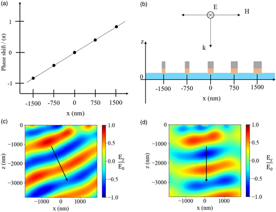
Figure 3(a) shows a designed discrete phase profile versus x for the deflector as five meta-atoms with fixed P = 750 nm and L = 3750 nm, where the phase is shifted over the range of L. Figure 3(b) shows a schematic image of the implemented DMSV consisting of five kinds of Mie resonators followed by the parameters in Fig. 1(c). We numerically simulated the deflection of transmitted optical waves at 1550 nm with normal incidence using the FDTD method and obtained the field distribution of the transmitted waves. Figures 3(c) and 3(d) show the y-component of the electric field in the x–z cross-sectional plane in the dielectric and metal phases of VO2, respectively. As shown in Fig. 3(c), in the case of the dielectric phase, the transmitted wave is deflected with θt = 24.4°, which is consistent with Eq. (2). On the other hand, in the metal phase, the transmitted wave propagates almost straight (θt ∼ 0°) with a transmittance of 27%, as shown in Fig. 3(d). Thus, switchable deflection versus temperature can be achieved for transmitted waves by a phase-change material. In addition, we can control the deflection angle by simply tuning L. We note that the transmittance and period of DMSV are trade-offs between the metal and dielectric phases (see supplementary data S4).
Fig. 3. (Color online) Switchable beam deflector: (a) discrete phase design via x position using generalized Snell's law, (b) a schematic image of the Mie resonator arrangement. The y-component of the electric field distribution of the transmitted waves at 1550 nm in the x–z cross section in the (c) dielectric and (d) metal phase of VO2. The arrows indicate the calculated deflection angle at (c) 24.4°, and (d) 0°.
Download figure:
Standard image High-resolution image
We have proposed a DMSV and demonstrated switchable wavefront control in transmission waves at 1550 nm. DMSV achieves a high phase contrast between 2π (the dielectric phase) and 0.5π (the metal phase) by a phase change of VO2. We have designed a switchable transmitted beam deflector using generalized Snell's law. It deflects incident optical waves with an angle of 24.4° in the dielectric phase, which then propagate almost straight in the metal phase. Such DMSV-based devices can be applied further to non-mechanical beam steering, active polarizers, active metalenses, etc. In addition, DMSV has wide versatility because the operation wavelengths and deflection angle can be adjusted.
Acknowledgments
This work was supported by JSPS KAKENHI grant number JP19H02630 and the JSPS Core-to-Core Program "Advanced Nanophotonics in the Emerging Fields of Nanoimaging, Spectroscopy, Nonlinear Optics, Plasmonics/Metamaterials and Devices".