
Abstract
Laser-assisted atom probe tomography was used to identify the impurity distribution in Si heterojunction (SHJ) solar cells composed of thin doped/intrinsic amorphous Si layers on the textured surface of a crystalline Si wafer. A site-specific lift-out technique involving a focused ion beam enabled the selection of a ∼2 × 2 μm2 area on an arbitrary pyramidal surface. The distributions of B, P and C in the amorphous Si layers introduced by p-type (trimethyl-borane or diborane) or n-type (phosphine) dopant gases were investigated. Standard guidelines for the assessment of the H content in amorphous Si of SHJ solar cells were provided.
Export citation and abstract BibTeX RIS
Photovoltaic modules based on Si solar cells have occupied a significant role in the solar cell market and have been researched to achieve cost-effectiveness and enhanced conversion efficiency in solar cells. 1,2) A Si heterojunction (SHJ) solar cell, which is composed of thin impurity-doped and intrinsic amorphous Si (a-Si) layers [also known as a heterojunction with intrinsic thin layer] 3) is a promising cell structure that enables both high conversion efficiency and low cost. 4,5) By using SHJs, the conversion efficiencies of Si solar cells have been increased by 21.5%, 6) 24.7% 7) and 25.1%. 8) Up to 2018, by introducing interdigitated back-contact into SHJs, higher efficiencies of 25.6% 9) and 26.7% 10,11) were achieved. For the development of SHJ solar cells with higher efficiency, the achievement of a high-quality a-Si layer is desired.
A commercial Si solar cell module features a pyramidal texture to effectively trap absorbed photons with near-bandgap energies. Si(111)-oriented surfaces are fabricated by alkaline solutions for crystalline Si(100) wafers, resulting in anisotropic etching of the front and rear surfaces. 12) Randomly distributed upright pyramid textures are widely employed at the mass production level due to their facile mask-less fabrication. 13) The conformal impurity doping of all textures is a crucial issue because the dopant concentration significantly determines the band structure around the doped/intrinsic interface. The common techniques used for measuring doping profiles on flat substrates encounter certain difficulties when analyzing such textures. To estimate the optimal doping conditions on the pyramidal surfaces, secondary ion mass spectrometry (SIMS) is widely used for profiling the elements along the depth direction of the layers developed on flat substrates. However, the elemental profiles on the pyramid surfaces in SHJs cannot be directly obtained by conventional methods. Recent successful attempts concerning SIMS analysis have been reported for determining the total number of dopants from multiple pyramids by tuning the incident primary ion beam. 14) In recent years, scanning nonlinear dielectric microscopy provided active dopant distributions from the cross-sectional pyramid. 15)
The direct observation of impurities from such a tiny region (i.e. a single pyramidal surface) is a challenging issue and is presumed to be reliable in determining optimal doping conditions. In addition, together with controlling the dopant concentration, the hydrogen (H) content in the a-Si of an SHJ should also be precisely controlled for the desired layer deposition on the textured surface. Atom probe tomography (APT) is a powerful tool for visualizing 3D elemental distributions in materials with a nearly atomic-scale resolution. 16) Combined with a site-specific lift-out obtained by a focused ion beam (FIB) technique, 17) dopant profiles at a desired location on Si-based electronic device structures can be obtained via APT. 18,19) A time-of-flight mass spectrometer equipped in APT is equally sensitive to all elements, and has the potential to detect H atoms in hydrogenated a-Si (a-Si:H) layers, as well as generally analyze the distribution of doped impurities. Although H quantification is a challenging issue in any material, several attempts at the direct detection of H in APT have been reported previously. 20–22) Because the impact of H in SHJ solar cells on the cell properties has been studied thus far, 23–26) a highly accurate quantitative analysis of the H that is incorporated into a-Si layers will be beneficial for creating desired products. Here, we report the successful experimental establishment of APT analysis combined with a site-specific FIB on a single pyramidal surface of actual SHJ solar cells. Based on this method, the atomic ratios of various dopants [boron (B) and phosphorus (P)] and H in p- and n-type a-Si layers were measured. For the p-type a-Si layer, two types of doping molecules, trimethyl-borane [B(CH3)3] and diborane (B2H6), which are commonly used as p-type dopant gases, 27–29) were investigated.
The SHJ sample employed in this study is shown in Fig. 1(a). Randomly Si(111)-faced pyramidal surfaces were generated by the alkaline etching of an n-type Czochralski Si(100) wafer, resulting in a characteristic angle of the texture of approximately 50°, as shown in Fig. 1(b), which is consistent with the previously recorded value. 30) For layer formation, an intrinsic a-Si (i-a-Si) thin layer was grown using SiH4 and H2 gases via plasma-enhanced chemical vapor deposition (PECVD), followed by p-type a-Si (p-a-Si) layer formation using B(CH3)3 or B2H6 gases. An n-type a-Si layer was formed using PH3 gas on the opposite side. An approximately 100 nm thick indium tin oxide layer acting as a transparent conducting oxide (TCO) layer was deposited on top of both sides. The silver electrode formation was processed for both sides, as shown in the inset of Fig. 1(a). All of the fabrication processes were conducted at low temperatures (< 200 °C). 7) The samples with p-a-Si layer introduced by B(CH3)3 or B2H6 are hereafter referred to as Samples 1 and 2, respectively. The conversion efficiency and open-circuit voltage of the SHJ solar cells employed in this work were above 22% and 730 mV, respectively.

Fig. 1. (Color online) (a) Scanning electron microscope (SEM) image tilted at 52° to the surface morphology for the randomly textured SHJ solar cell employed in this work. (b) Cross-sectional view of a single pyramid. (c) Schematic illustration of the ideal needle position for adapting APT measurements on a single pyramid slope. (d) SEM image of the final shape of the needle specimen. TCO layer approximately 50 nm thick remains on top of the a-Si/Si substrate.
Download figure:
Standard image High-resolution imageFor lifting out and fabricating APT needle specimens, a Ga FIB with a dual-beam system (Helios NanoLab600i, Thermo Fisher Scientific) was utilized. The ideal needle-specimen position shown in Fig. 1(c) is expected to be the best direction for obtaining abrupt elemental distributions with the highest depth resolution in the APT analysis. 31) The specimens were sharpened into needles using annular milling patterns based on in situ SEM observations, resulting in the detection of a TCO layer approximately 50 nm thick on top of the a-Si/Si substrate, as shown in Fig. 1(d). A laser-assisted local-electrode atom probe (LEAP4000XHR, AMETEK) equipped with a UV laser (wavelength: 355 nm) was employed. The base temperature of the sample stage was stabilized at 35 K. The laser pulse rate and power were 100 and 160 kHz and 30 pJ, respectively. The 3D reconstruction of the APT data was carried out using Cameca integrated visualization and analysis software (IVAS) based on published algorithms. 32)
Figure 2(a) displays atom maps of the main elements of In, O, Si, H, B and SiO in the SHJ solar cell with p-a-Si layer doped with B(CH3)3 gas (Sample 1). The identity of all ions was determined from the mass-to-charge-state ratio [measured in units of Daltons (Da)], hereinafter referred to as the mass spectrum, as shown in Fig. 2(b). The In and O atoms appear in the TCO layer on top of the Si matrix. A large amount of H originates from the a-Si layer. A distribution of B atoms is found in the top a-Si layer, and a few dots appear in the bottom a-Si layer. The clear presence of double SiO layers is an excellent marker for identifying the interfaces of TCO/p-a-Si and i-a-Si/Si substrates, which were introduced as native oxides during the growth process.
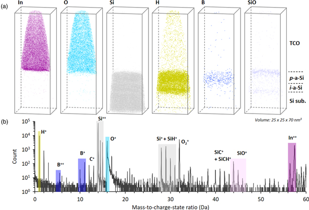
Fig. 2. (Color online) (a) 3D atom maps of In (56.5, 57.5, 113 and 115 Da), O (16 Da), Si (14, 14.5, 15, 28, 29 and 30 Da), H (1 Da), B (5.5, 6, 10 and 11 Da) and SiO (44, 45 and 46 Da) in Sample 1. (b) Mass spectrum for the entire atom map shown in (a).
Download figure:
Standard image High-resolution imageFor comparison of the quantities of C incorporated in the p-a-Si layer grown by B(CH3)3 and B2H6 gases (Samples 1 and 2, respectively), a series of mass spectra around the peak positions for B+ and C+ (9–13.5 Da) and SiC+ (39–43.5 Da) are summarized in Fig. 3. C-related peaks, such as CH, SiC and SiCH, are evidently found in Sample 1 [Fig. 3(a)], while limited C-related peaks exist in Sample 2, as expected [Fig. 3(b)]. A detailed assessment of the H contribution in the a-Si layer will be discussed later. To deduce the ratio of C to B in Sample 1, only the peak interference position at 12 Da overlaying both 11BH+ and 12C+ should be considered, while other peaks separately appear for B and C. By considering 10B+, 11B+ and 10BH+ (10 and 11 Da) for B, and 12CH+, 28SiC+, 29SiC+, 28SiCH+, 30SiC+, 29SiCH+ and 30SiCH+ (13, 40, 41, 42 and 43 Da) for C, the ratio of C/B was calculated to range from 1.5–2.7, less than the original stoichiometric ratio of B(CH3)3 (i.e. a C/B of approximately 3) even at its maximum value. It is speculated that C-related molecules were desorbed as gas during layer formation.

Fig. 3. (Color online) (a) Mass spectra around the peak positions for B+ and C+ (9–13.5 Da) and SiC+ (39–43.5 Da) in the p-type a-Si layer of (a) Sample 1 and (b) Sample 2.
Download figure:
Standard image High-resolution imageFigure 4(a) shows the overlaid atom maps of O, Si, H and B in the SHJ solar cell doped with B2H6 gas (Sample 2). The mass spectra around the B+ and Si+ peaks ranging from 9–11.5 Da and 27–31.5 Da, respectively, are summarized in Fig. 4(b). Because of the large amount of H present in the a-Si layer, both B-H and Si-H molecules were detected. To precisely estimate the actual amounts of H, B and Si, a peak decomposition analysis was conducted based on the isotopic natural abundance of these elements: 10B:11B = 19.9:80.1 and 28Si:29Si:30Si = 92.22:4.69:3.09. 33)

Fig. 4. (Color online) (a) 3D atom map of O, Si, H and B (doped using B2H6 gas) in a stack of TCO/a-Si/Si substrates and a cylindrical volume (10 nmφ × 40 nm) for analyzing 1D profiles. (b) Mass spectra around B+ and Si+ peaks extracted from the cylindrical volume shown in (a). (c) 1D concentration profiles of O, B and H.
Download figure:
Standard image High-resolution imageFigure 4(c) shows the O, B and H profiles obtained from the cylindrical region displayed in Fig. 4(a). All O atoms were extracted from O+ (16 Da), O2 + (32 Da) and SiO+ (44, 45 and 46 Da). The precise quantification of O species in oxide layers remains a serious issue due to the significant loss of O during evaporation, 34) such as via the partial desorption of O as neutral O2 in APT. 35) A large amount of O was detected in the TCO layers up to a distance of ∼18 nm. The presence of O at distances of ∼25 and ∼35 nm provides us with a method for identifying the p-a-Si/i-a-Si and i-a-Si/Si substrate interfaces, respectively. B atoms of 5 at.% at maximum are distributed in the p-a-Si layer, and undesired B atoms are found in the i-a-Si layer. This may plausibly be due to contamination from the unavoidable B atoms adhered to the wafer carrier that was present during the i-a-Si layer growth due to its thermal instability. 36) However, with respect to the B concentration of around 5 at.%, it is higher than the ranges normally used. 37) The present p-a-Si layers were formed with high B2H6 gas phase concentration ratio for achieving sufficiently high active dopant concentration. Although the B concentration in the a-Si is not completely constant (referred to as the p-a-Si layer), one can separately identify the i-a-Si layer beneath the p-a-Si layer and highly B-doped p-a-Si layer. The non-uniform B distribution is probably due to the non-stabilized vapor phase of B2H6 gas concentration in the deposition chamber, which is supported by SIMS measurement. Conversely, few B atoms were detected in the i-a-Si layer of Sample 1 (not shown here), suggesting that it is reasonable to use B(CH3)3 gas to avoid B incorporation in the i-a-Si layer. 27) With respect to the H atoms detected in APT, residual H gas adsorbed on the needle-specimen field evaporates during the analysis, resulting in the occurrence of a background signal when attempting to detect the H present in the actual specimen. 38) Nevertheless, a large number of H atoms appear in the a-Si layer, as displayed in Fig. 2(a). The H concentration, ranging from 5 at.%–10 at.%, appears over the entirety of the a-Si layer, while its concentration in the Si substrate is negligibly low and equivalent to the background level for crystalline Si. H atoms tend to segregate at the interfaces of the TCO/p-a-Si, p-a-Si/i-a-Si and i-a-Si/Si substrates.
The data set for the n-a-Si layer was obtained on the opposite side from which the data for p-a-Si of Sample 2 was obtained. Figure 5(a) shows the entire atom map for O, Si, H and P (doped by PH3 gas) in a stack of TCO/a-Si/Si substrates. Based on the peak ratio in the Si substrate considering the natural abundance of Si isotopes, as shown in (iii) of Fig. 5(b), additional peak counts associated with H are present at 29, 30 and 31 Da in the i-a-Si layer, which is similar to that of Sample 2, as shown in Fig. 4(b). In the n-a-Si layer, the peak at 31 Da is considerably higher compared to that in the i-a-Si layer, thereby demonstrating the presence of P.

Fig. 5. (Color online) (a) 3D atom map of O, Si, H and P (doped using PH3 gas) in a stack of TCO/a-Si/Si substrates and three cylindrical volumes (20 nmφ × 2 nm) for elemental composition analysis. (b) Mass spectra around SiH+ and P+ in the (i) n-a-Si, (ii) i-a-Si and (iii) Si substrates. (c) 1D concentration profiles of O, P and H extracted from the cylindrical volume 10 nmφ × 20 nm shown in the inset of the atom map.
Download figure:
Standard image High-resolution image
Figure 5(c) shows the 1D concentration profiles of O, P and H extracted from the cylindrical volume of 10 nmφ × 20 nm shown in the inset of the atom map. The original P content (P++ and P+ shown at 15.5 and 31 Da, respectively) can be extracted using a peak decomposition method and calculated in the same manner as in Fig. 4(c). P atoms of 3 at.% at maximum are distributed in the n-a-Si layer, and a small amount of P in the i-a-Si layer presumably originates from the residual PH3 gas in the PECVD chamber that was present during the growth of the i-a-Si layer. H atoms tend to segregate at the interfaces of the TCO/n-a-Si, n-a-Si/i-a-Si and i-a-Si/Si substrates. The H concentration in the n-a-Si layer ranges from 10 at.%–15 at.%, while its concentration in the Si substrate is negligibly low, which is a similar trend to that shown in Fig. 4(c). Although the interpretation of H detection results has been systematically investigated under various APT conditions, 39) the high content of H for the a-Si layers compared to that in the Si substrate is presumed to be accurate in the present analysis. This may represent the standard ranges of H ratios in the a-Si:H layer within similar SHJ systems. An accurate quantification method for H has not yet been agreed upon. However, our present H concentration ranges are consistent with the reported values obtained by infrared spectroscopy. 40) A more reliable quantification method should be investigated in future research.
In summary, APT was utilized to identify the 3D distribution of impurities in SHJ solar cells composed of doped/intrinsic a-Si layers on the pyramidal-textured surface. A site-specific FIB enabled the selection of an approximately 2 × 2 μm2 area on a single pyramidal surface. Based on this method, the atomic ratios of dopants (B, C and P) in the a-Si layers were investigated. We assessed a method for H quantification, which may represent an adequate standard for the H content in the a-Si:H layer within the SHJ system.
Acknowledgments
The authors would like to thank R. Shibahara for technical support. This work was supported in part by the New Energy and Industrial Technology Development Organization under the Ministry of Economy, Trade and Industry.