

Abstract
We report GaN-based vertical-cavity surface-emitting lasers (VCSELs) with buried GaInN tunnel junctions (TJs). Under room-temperature continuous-wave operation, the VCSEL with an 8 μm aperture exhibited a low operating voltage of 5.3 V at 10 kA cm−2 and a differential resistance of 110 Ω. In addition, the VCSEL with a 10 μm aperture showed a threshold current of 14.4 mA and a peak output power of 2.0 mW. An influence of an absorption loss at the GaInN TJ on laser performance was estimated using an analysis of a one-dimensional optical intensity profile based on a cross-sectional STEM image.
Export citation and abstract BibTeX RIS
Vertical-cavity surface-emitting lasers (VCSELs) have attracted a lot of attention because of many advantages, such as no catastrophic optical damage, circular beam profiles, and small temperature dependences of lasing wavelengths. 1) Recently, GaN-based VCSELs have been actively developed 2,3) for applications to adaptive headlamps and retinal scanning displays. GaN-based VCSELs have been reported to have various cavity structures 2–7) and have a wide range of wavelengths from UV 8,9) to green, 10–12) and most of them use indium tin oxide (ITO) as a p-type ohmic intracavity contact layer. Since an ITO is known to have a considerably large absorption coefficient in the visible region, 13,14) it is a fundamental issue limiting performances of GaN-based VCSELs. Furthermore, it has been reported that VCSELs using ITO intracavity contacts (ITO-VCSELs) could have problems in terms of long-term reliability. 15) Several groups have expected that tunnel junction (TJ) could solve these problems. 6,15) There have been several reports on GaN-based VCSELs using GaN TJs. 6,15,16) Lee et al. have achieved a room-temperature (RT) continuous-wave (CW) lasing operation of the VCSEL with a buried tunnel junction (BTJ) of GaN on an m-plane GaN substrate, showing an optical output power of 0.72 mW. 16) Shen et al. also have obtained an output power of 2.1 mW in a GaN TJ-VCSEL with a Si diffusion current confinement aperture. 15) Although RT CW operations have been successfully demonstrated, these devices still operate at high voltages, ∼7.2 V at 10 kA cm−2. This is attributed to a relatively large depletion region thickness resulting from the large band gap of GaN. 17–20) On the other hand, GaInN TJs can significantly reduce resistance because GaInN has not only a narrow band gap but also a potentially large polarization field due to piezoelectric effect. 21–24) Although a large absorption coefficient of GaInN with a high InN mole fraction is concerned, 25) its impact on device characteristics could be minimized. This is because a GaInN layer in a GaInN TJ is much thinner (several nm at most) than an ITO layer (20 nm at least). However, there has been no report discussing an influence of absorption loss introduced by GaInN TJs on GaN-based VCSELs. In this letter, we discussed the influence of absorption loss of the GaInN TJ and demonstrated RT CW operations of GaN-based VCSELs with GaInN buried tunnel junctions (BTJ-VCSELs), comparing with an ITO-VCSEL.
A schematic of a 5.5λ-cavity BTJ-VCSEL is shown in Fig. 1(a). The GaN-based layers were grown on a c-plane GaN substrate only by metalorganic vapor phase epitaxy (MOVPE). The cavity structure consisted of a 40-pair AlInN/GaN bottom distributed Bragg reflector (DBR), a 5.5-λ cavity, and an 8-pair SiO2/Nb2O5 top DBR. The center wavelengths of both the DBR stopbands were located at 410 nm. The 5.5-λ cavity composed of a bottom n-GaN layer, 5-pair GaInN/GaN multiple quantum wells emitting at 400 nm, a p-Al0.2Ga0.8N electron blocking layer, a p-GaN layer, a p++-Ga0.75In0.25N (2 nm, [Mg]: 2 × 1020 cm−3), a n++-GaN (5 nm, [Si]: 6 × 1020 cm−3), and a top n-GaN. The heavily Mg-doped GaInN layer of the TJ was designed to place at the node of the optical intensity profile to reduce absorption loss. At the same time, two growth steps were carried out to form the GaInN BTJ. The first epitaxial growth up to the GaInN TJ was performed on the GaN substrate. After taking the wafer out of the MOVPE reactor, TJ mesas with 6–10 μm diameters and ∼10 nm depths were formed by reactive ion etching (RIE) as current apertures. As the second growth, the top n-GaN layer was grown in order to bury the TJ mesas. Next, the top n-GaN layer was partially etched until the bottom n-GaN layer to form 36–40 μm diameter device mesas. The lateral Mg activation 26) was followed by depositions of the SiO2 insulating layer and the top and bottom ring Cr/Ni/Au n-electrodes. Finally, the 8-pair SiO2/Nb2O5 DBR was deposited on top of the top n-GaN surface. We evaluated current–voltage–light output power (I–V–L) characteristics, emission wavelength spectra, and polarization characteristics under RT CW operations. For comparison, we used our previously reported 4λ-cavity ITO-VCSEL 27) to compare the characteristics. The current aperture of the ITO-VCSEL consisted of a combination of a 20 nm ITO electrode and a 10 nm SiO2 insulating layer with an 8 μm aperture. Note that differences between the BTJ-VCSEL and the ITO-VCSEL discussed here were not just the current aperture but also the cavity length as shown in Figs. 1(a) and 1(b).

Fig. 1. (Color online) Schematics of the VCSEL with (a) GaInN BTJ aperture and (b) ITO intra-cavity contact.
Download figure:
Standard image High-resolution imageWe calculated internal losses introduced by the GaInN TJ and the ITO contact in the above-mentioned VCSELs by using one-dimensional transmission matrix method (1D TMM). Table I shows material constants used in the calculation. The 2 nm p++-GaInN and the 20 nm ITO were placed at the node of the optical intensity profile in the cavity to minimize absorption losses. We applied the energy shift method proposed by Bergmann et al. to calculate refractive index of AlGaN and GaInN. 28) The absorption coefficient was roughly estimated by a method proposed by Huang et al. using a simple linear function of doping level. 29) Figure 2 shows the internal losses as a function of positions of the GaInN TJ and the ITO electrode, respectively. The designed positions correspond to 0 nm on the horizontal axis. The result indicates the internal loss is reduced from 2.8 cm−1 to 0.3 cm−1 by using the GaInN TJ instead of ITO. On the other hand, the internal loss of the BTJ-VCSEL increases sharply compared with that of the ITO-VCSEL when the GaInN layer and the ITO deviate from the designed positions, which suggests that BTJ-VCSELs require more precise control of the layer thickness.
Table I. Summary of material constants used in the one-dimensional transmission matrix simulation of 410 nm cavity mode. 13,25,28–32)
| Layer | |||||||||
|---|---|---|---|---|---|---|---|---|---|
| ITO-VCSEL | BTJ-VCSEL | Doping conc. (cm−3) | Abs. Coeff., (cm−1) | Refractive index | Thickness (nm) | ||||
| 8-pair SiO2/Nb2O5 DBR | NA | 0 | 1.469/2.545 | 69.8/40.3 | |||||
| spacer Nb2O5 | top n-GaN | NA | 1 × 10¹⁹ | 0 | 5 | 2.545 | 2.506 | 30.3 | 280.3 |
| ITO | TJ n++-GaN | NA | 6 × 10²⁰ | 2000 | 300 | 2.164 | 2.506 | 20 | 5 |
| p++-GaN | TJ p++-GaInN | 3 × 10²⁰ | 2 × 10²⁰ | 750 | 100000 | 2.506 | 2.599 | 10 | 2 |
| p-GaN | 4 × 10¹⁹ | 100 | 2.506 | 51.99 | 68.1 | ||||
| p-AlGaN | 2 × 10¹⁹ | 50 | 2.431 | 20 | |||||
| GaN barrier | UID | 0 | 2.506 | 6 | |||||
| 5 × GaInN QW | UID | 0 | 2.734 | 3 | |||||
| bottom n-GaN | 1×10¹⁹ | 5 | 2.506 | 423.7 | |||||
| 40-pair AllnN/GaN DBR | UID | 0 | 2.267/2.506 | 45.2/40.9 | |||||

Fig. 2. (Color online) Internal loss in the cavity as functions of position of a p++-GaInN for a BTJ-VCSEL and an ITO for an ITO-VCSEL.
Download figure:
Standard image High-resolution imageFigure 3 shows I–V–L characteristics for the GaInN BTJ-VCSELs having the 6-, 8-, and 10 μm apertures and the ITO-VCSEL having the 8 μm aperture. We observed abrupt light output power increases for all the VCSELs. Figure 4(a) shows emission spectra of the BTJ-VCSEL with the 6 μm diameter aperture at 7 and 10 mA. It shows a very narrow emission spectrum (FWHM: 0.05 nm) at 410.8 nm. Figure 4(b) shows light output power values of the same VCSEL as a function of a polarizer angle at 12 mA, indicating that the emission light was linearly polarized. The other VCSELs also showed similar characteristics. Based on these results, we conclude that we have achieved RT CW operations of the GaN-based VCSELs with the GaInN BTJs. The threshold currents for the 6-, 8-, 10 μm aperture BTJ-VCSELs were 8.5 mA, 10.9 mA, and 14.4 mA, respectively. The maximum light output powers were 1.9 mW, 1.6 mW, and 2.0 mW, respectively. On the contrary, our typical ITO-VCSEL with the 8 μm aperture showed a threshold current of 7 mA and the maximum output power of 3.0 mW. At this moment, the BTJ-VCSEL with the 8 μm aperture had a higher threshold current and a lower slope efficiency than those of the ITO-VCSEL.
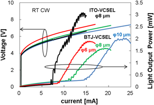
Fig. 3. (Color online) I–V–L characteristics of GaInN BTJ-VCSELs with 6-, 8-, and 10 μm apertures and an ITO-VCSEL with an 8 μm aperture under RT CW operations. 27) Since no anti-reflectance coating was deposited on the backside of the substrate, observed oscillations on the I–L curves were interference fringes due to a reflection of the substrate backside.
Download figure:
Standard image High-resolution image
Fig. 4. (Color online) (a) Emission wavelength spectra and (b) polarization characteristics of the fabricated GaInN BTJ-VCSEL with the 6 μm diameter current aperture.
Download figure:
Standard image High-resolution imageWe here discuss reasons for such inferior characteristics of the GaInN BTJ-VCSELs. We observed no light emission outside the TJ apertures, so that a leakage current outside the aperture seems insignificant for the device performance of the BTJ-VCSELs. Next, we assumed the injection efficiencies of both the devices were the same because of the same active region design. Considering comparable mirror loss between both the VCSELs (calculated value were 5.6 cm−1 for the BTJ-VCSEL and 6.8 cm−1 for the ITO-VCSEL), the BTJ-VCSEL should contain an unintended increase in internal loss. We performed cross-sectional STEM analysis to check a deviation of a thickness of each layer in the cavity from the designed value. The STEM analysis shows that the fabricated BTJ-VCSEL had a 6.5 nm thicker cavity than the designed cavity. The contributions to the deviation were +12.6 nm for the bottom n-GaN, −0.9 nm for the p-(Al)GaN, and −5.2 nm for the top n-GaN. Figure 5 shows the cross-sectional STEM image of the BTJ-VCSEL overlaid with profiles of a refractive index and a calculated optical intensity in the resonance mode. Note that we recalculated the optical intensity profile using the measured layer thicknesses obtained from the STEM analysis. As a result, the layer thickness deviation should cause not only a ∼33 cm−1 internal loss at the GaInN TJ but also decrease an optical confinement factor from the designed value of 1.76% to 1.39% in the cavity direction. Here, the optical confinement factor was given by Γz = ∫da ∣E(z)∣2 dz/∫L ∣E(z)∣2 dz, where L, d a , E(z) are an effective cavity length, a thickness of the active region, and an electric field as a function of position, z, respectively. These factors could lead to the measured high threshold current and low slope efficiency values of the BTJ-VCSELs at this time.

Fig. 5. (Color online) The cross-sectional STEM image of the BTJ-VCSEL overlaid with profiles of a refractive index and a calculated optical intensity in the resonance mode.
Download figure:
Standard image High-resolution image
On the other hand, the BTJ-VCSEL having 8 μm aperture exhibited an operating voltage of 5.3 V at 10 kA cm−2 and a differential resistance of 110 Ω, which were equivalent to that of the ITO-VCSEL. Additionally, this voltage was lower than the GaN BTJ-VCSEL reported by Shen et al. 15) and by Lee et al. 16) This is because the use of GaInN with a narrower depletion layer thickness due to the small band gap and the large polarization electric field, thereby increasing a tunneling probability.
In summary, the 5.5λ-cavity GaN-based VCSELs with the GaInN BTJs was designed and fabricated. The 1D TMM simulation predicted the GaInN BTJ-VCSEL can reduce internal loss by 2.5 cm−1 compared to that of the ITO-VCSEL. RT CW operations of the GaInN BTJ-VCSEL were achieved, showing a low operating voltage of 5.3 V at 10 kA cm−2 and a differential resistance of 110 Ω for the 8 μm aperture case. The maximum output power reached 2.0 mW for the VCSEL with the 10 μm diameter aperture. More precise thickness control should lead to improvements of GaInN BTJ-VCSELs.
Acknowledgments
This work was supported by the MEXT "Research and development of next-generation semiconductor to realize energy-saving society" Program Grant Number JPJ005357, the MEXT Private University Research Branding Project (2016-2020), and the JSPS KAKENHI for Scientific Research A [20H00353].