

Abstract
A 100 nm wide superconducting niobium (Nb) interconnect was fabricated by a 300 mm wafer process for Cryo-CMOS and superconducting digital logic applications. A low pressure and long throw sputtering was adopted for the Nb deposition, resulting in good superconductivity of the 50 nm thick Nb film with a critical temperature (Tc) of 8.3 K. The interconnects had a titanium nitride (TiN)/Nb stack structure, and a double-layer hard mask was used for the dry etching process. The exposed area of Nb film was minimized to decrease the effects of plasma damage during fabrication and atmosphere. The developed 100 nm wide and 50 nm thick Nb interconnect showed good superconductivity with a Tc of 7.8 K and a critical current of 3.2 mA at 4.2 K. These results are promising for Cryo-CMOS and superconducting digital logic applications in the 4 K stage.
Export citation and abstract BibTeX RIS
1. Introduction
Quantum computers using qubits can execute certain algorithms faster than classical computers. 1,2) In a superconductor-based quantum computer system, the qubits must be cooled down to 10 mK to minimize thermal noise. And they require additional control/readout electronics which are controlled by RT devices. It is considered more than two I/O (Input and Output) cables are required for one qubit. To increase the scale of quantum computers, there exists important issues of I/O bottleneck and cooling capacity because space and cooling capacity are limited in dilution refrigerators.
One potential solution to solve the issues is to employ cryogenic CMOS (Cryo-CMOS) at the 4 K stage and reduce the number of I/O cables connecting from RT to cryogenic temperatures. 3–8) Figure 1 shows a schematic image of future quantum computing systems. The quantum–classical interface (QCI) using cryo-CMOS is desired to control/read-out the qubits. However, the cooling capacity at the 4 K stage is limited to around 1 ∼ 3 W, in which the reduction of the power consumption of the Cryo-CMOS is key to realizing an energy-efficient control/readout system for the qubits. The introduction of embedded nonvolatile resistive switching devices 9–15) is one of the significant focuses to reduce the power consumption of the Cryo-CMOS circuit. 16) The small input capacitance of the resistive switching device with the crossbar architecture has great potential not only for RT operation but also for cryogenic temperature one to improve the energy efficiency of QCI chips using cryo-CMOS.

Fig. 1. Schematic image of quantum computing systems. The quantum–classical interface (QCI) using cryo-CMOS is desired to control/read-out the qubits in future quantum computing systems.
Download figure:
Standard image High-resolution imageSuperconducting interconnects are challenging but are expected to drastically enhance the performance of the IC of Cryo-CMOS. If higher operation frequencies are achieved using the superconducting interconnects, it is possible to reduce the operating voltage while keeping the same operating frequencies at RT, resulting in a decrease in power consumption. In superconducting digital electronics, multi-layered Nb interconnects are used. Hidaka et al. reported the fabrication process of 9 layer Nb interconnects with a minimum linewidth of 1 μm using i-line photolithography. 17) Tolpygo et al. also reported the fabrication process of 8 layer Nb interconnects whose minimum dimensions are 500 nm for linewidth and 700 nm for space using 248 nm photolithography. 18)
In Si CMOS fabrication, it is demanded to reduce interconnect pitch to increase circuit density. Out target FPGA is designed and fabricated in a 65 nm node standard CMOS platform, 16) then, a pitch of the superconducting interconnect must be reduced further. Y. W. Kim et al. fabricated narrower Nb interconnects by lift-off technique with e-beam lithography. 19) However, the superconductivity of the Nb interconnect drastically degraded when linewidth was reduced below 200 nm. The 100 nm wide Nb line with a thickness of 50 nm has a critical current density (Jc) of below 2 MA cm−2, therefore, the line could flow a superconducting current of below 0.1 mA. Pokhrel et al. fabricated Nbx Ti(1−x)N superconducting interconnects by a 300 mm CMOS compatible process. 20) The fabricated interconnect had dimensions of 50 nm in width and 50 nm in thickness and had a critical current (Ic) of 0.15 mA. When considering the utilization of superconducting interconnects in Si LSIs, fundamental challenges arise in the need to scale down wirings below a 200 nm pitch while preserving superconducting properties such as Ic at 4.2 K in these scaled-down fine wires.
In this paper, we have developed superconducting Nb interconnects to replace Cu interconnects at cryogenic temperatures for Cryo-CMOS. A 300 mm CMOS and back-end-of-line (BEOL) compatible processes are applied for the fabrication of the Nb wiring with 200 nm pitched. Superconducting critical temperature (Tc) and Ic of the Nb interconnects were evaluated.
2. Experiment
We have developed a fabrication process for superconducting Nb interconnects, and the fabrication is compatible with a standard 300 mm CMOS process. A TiN/Nb stacked structure and a double-layer hard-mask process were adopted to protect the Nb layer from plasma damage during fabrication.
The fabrication flow is shown in Figs. 2(a)–2(e). First, a 50 nm Nb and 25 nm TiN stack were deposited on a thermally oxidized 300 mm wafer by DC magnetron sputtering. A low pressure (Ar pressure of 0.02 Pa) and long throw (target-substrate distance of 240 mm) technique were adopted for the Nb deposition with a water-cooled substrate stage. The sputtering conditions corresponded to the "Zone-T" of the structure zone model developed by Thornton. 21,22) The substrate temperature (T) during depositions was assumed about 300 K by the water-cooled stage, and the mp (Tm) of Nb is 2750 K, then T/Tm was 0.11. In addition, the Ar pressure of 0.02 Pa was low enough for "Zone-T." It is expected the film deposited under the "Zone-T" condition has a structure of densely packed fibrous grains without voids. It has the advantage of preventing gas absorption and oxidation during/after fabrication.
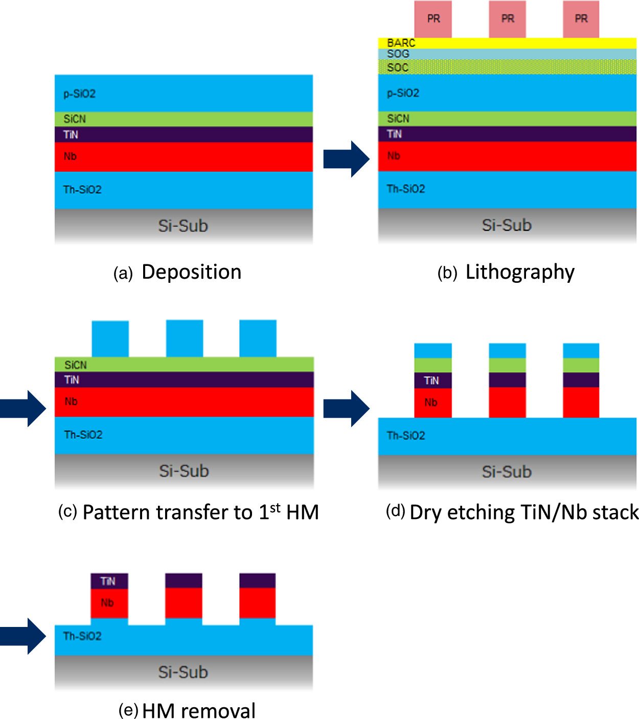
Fig. 2. Fabrication flow for superconducting Nb interconnects. A TiN/Nb stacked structure and a double-layer hard mask process were adopted to protect the Nb layer from plasma damage during fabrication.
Download figure:
Standard image High-resolution imageNext, a double-layer layer hard-mask (HM) of p-SiCN and p-SiO2 was formed by plasma-enhanced CVD (PECVD) at 350 °C [Fig. 2(a)]. After coating the pattering layers of SOC, SOG, and BARC, liquid immersion argon fluoride (ArF) excimer laser lithography was carried out for patterning lines [Fig. 2(b)]. Then, the line patterns were transferred to the 1st HM of the p-SiO2 layer by dry-etching, and then, the photoresist was removed by an oxygen plasma ashing process [Fig. 2(c)]. Next, the line patterns were transferred to the 2nd HM of the SiCN layer, and then TiN and Nb layers were formed into the line patterns by dry etching [Fig. 2(d)]. Finally, the hard mask layer was removed completely to probe pads for electrical measurement [Fig. 2(e)].
We have developed two types of etching gas systems, Cl2/BCl3 and CF4/N2, for the double HM of the TiN/Nb pattering. The optimized etching rates of each material are listed in Table I. It was shown that Cl2/BCl3 chemistry is suitable for etching TiN/Nb stack because it had high selectivity to the HM materials. On the other hand, CF4/N2 chemistry can etch HM materials much faster than TiN. Therefore, after etching the TiN/Nb stack, residual HM is removed completely with a CF4/N2 etching. Consequently, The TiN layer is entirely exposed [Fig. 1(e)]. The developed process could minimize the influence of plasma damage to the Nb interconnects by exposing only the surfaces on the side wall of Nb to the etching plasma.
Table I. Etching rate and selectivity ratios.
| Metal etch recipe | Dielectric etch recipe | |||
|---|---|---|---|---|
| Materials | Cl2/BCl3 | Selectivity | CF4/N2 | Selectivity |
| TiN | 178.2 nm m−1 | 8.6 (to SiCN) | 21.5 nm m−1 | — |
| Nb | 169.2 nm m−1 | 8.1 (to SiCN) | 67.2 nm m−1 | — |
| SiCN | 20.7 nm m−1 | — | 199.8 nm m−1 | 9.2 (to TiN) |
| p-SiO2 | 80.4 nm m−1 | — | 115.2 nm m−1 | 5.3 (to TiN) |
We prepared line-and-space (L&S) patterns with seven different pitches of 200, 400, 800, 1000, 1600, 2000, and 4000 nm. The line width is half of the pitch, and the line lengths are 15 mm, except for the 4000 nm pitched line whose length is 14.4 mm. After the fabrication of TiN/Nb interconnects, the devices were observed and checked morphology by critical dimension scanning electron microscope (CD-SEM) and SEM. Next, electrical measurements were carried out. The line resistance for 25 devices was measured by the four-probe method at RT and sheet resistance was calculated. Then, a few selected samples, which have median values of RT resistance were characterized by low temperature measurement. The devices were cooled in a liquid He dewar, and Tc and Ic were studied.
3. Results and discussion
3.1. Morphological observation
Figure 3(a) shows a CD-SEM image of the fabricated 200 nm pitched L&S patterns of the TiN/Nb stacked structure. It is shown that lines are separated completely with a designed dimension. Figure 3(b) shows a bird's-eye view SEM image, and the surfaces had smooth morphology without redeposited materials or etching residues. Figure 3(c) shows a side-view SEM image, and it shows that approximately 21 nm of TiN remained, completely covering Nb. As a result, the thin Nb layer was protected from plasma damage during fabrication by the TiN layer.
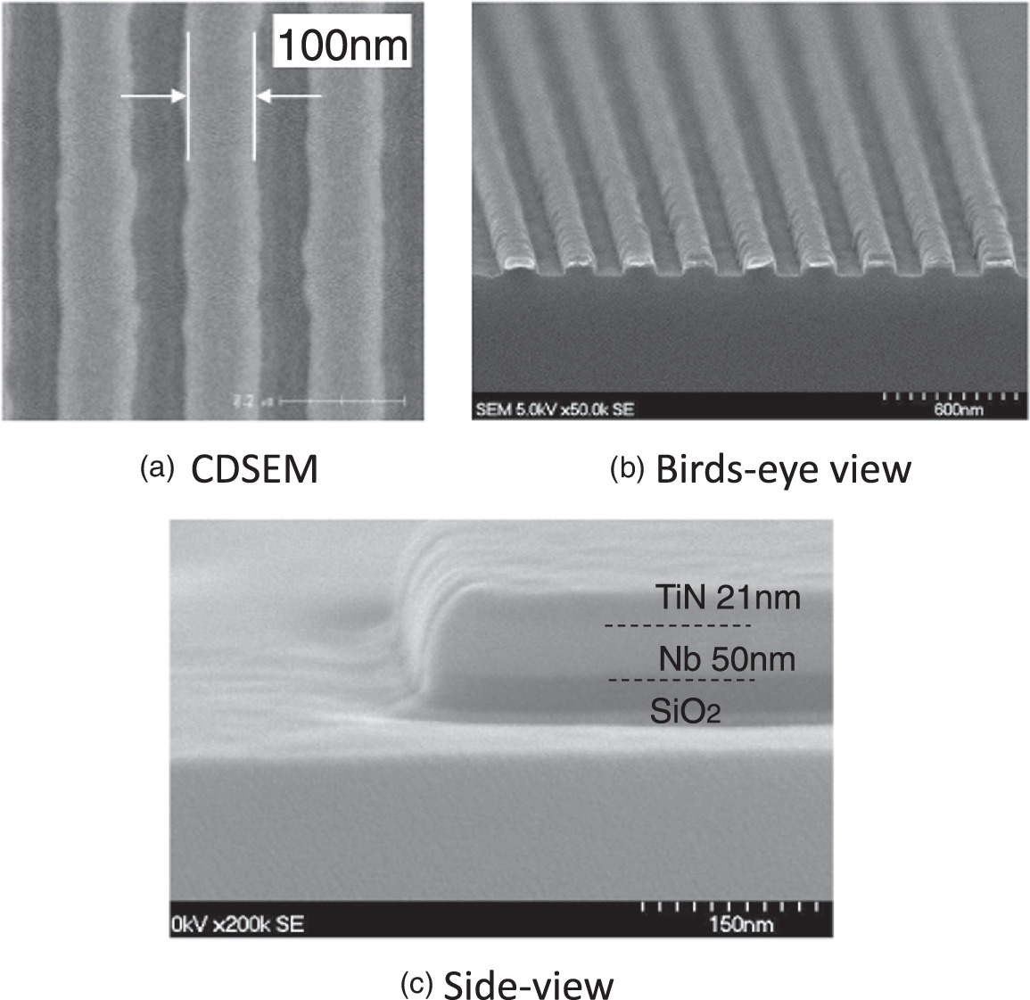
Fig. 3. SEM observation of Fabricated Nb interconnects with a TiN/Nb stacked structure. CD-SEM image (a), bird's-eye view (b), and side-view image (c). The surface had smooth morphology without redeposited materials or etching residues. Approximately 21 nm of TiN remained, completely covering Nb.
Download figure:
Standard image High-resolution image3.2. Room temperature measurements
Figure 4 shows the sheet resistance of the TiN/Nb stack interconnects as a function of the designed line width. The sheet resistance of 3.8 ohm sq−1. is obtained in the wider lines. As the wire width decreases, the sheet resistance increases due to the small size effect and electron scattering from the side walls. 23) The sheet resistance changes gradually with linewidth, then, it shows there are no breaking or shorting. It is confirmed that 100 nm wide TiN/Nb interconnects are successfully fabricated.

Fig. 4. Sheet resistance of the TiN/Nb stack interconnects as a function of the designed line width. It is confirmed that 100 nm wide TiN/Nb interconnects are successfully fabricated without breaking or shorting.
Download figure:
Standard image High-resolution image3.3. Low temperature measurements
Next, superconducting critical temperature (Tc) was measured for the as-deposited 50 nm thick Nb film. The electrical contacts were made by bonding Al wires directly on the Nb surface. The Nb film showed superconductivity at 8.3 K. The Nb interconnects with the TiN/Nb stack structure were also characterized at low temperatures. A 100 nm wide Nb interconnect had a Tc of 7.8 K, and it showed excellent superconductivity with an Ic of 3.2 mA at 4.2 K, and a Jc of 64 M A cm−2 was obtained. A line width dependence of Tc is plotted in Fig. 5. In Fig. 5, the dotted line indicates Tc of the as-deposited 50 nm thick Nb film. It was found that Tc decreased with a reduction of line width.

Fig. 5. Line width dependence of Tc for fabricated Nb interconnects with a TiN/Nb stacked structure. It was found that Tc decreased with a reduction of line width.
Download figure:
Standard image High-resolution image
The most reported bulk Tc of Nb is 9.2 K. The Tc of our as-deposited Nb film was slightly decreased from the bulk value. The film thickness is very thin and close to a coherence length of about 40 nm. Some groups reported that the Tc of Nb film decreased as the thickness decreased. 24–29) Gubin et al. reported Tc of Nb film gradually decreased with a reduction of the thickness from 300 to about 50 nm, and the Tc of their 50 nm thick film was below 9 K. 24) The interpretation of the results was based on the proximity effect by the surface and film-substrate interface layers, of which superconductivity deteriorated. Therefore, the obtained Tc of 8.3 K for as-deposited film is a reasonable value due to the proximity effect.
Y. W. Kim et al. reported Tc and Jc decreased steeply for narrow Nb lines and discussed the non-ideal profile of the line edge of the samples fabricated by the lift-off process with e-beam lithography. 19) In our fabrication, the Nb film was deposited by low pressure and long throw sputtering for densely packed fibrous grain structure and patterned into L&S by dry etching process with the double layer HM. Then, the edge profiles were very smooth without redeposited materials, etching residues, or large grain boundaries as shown in Figs. 3(a)–3(c). Consequently, as the line width reduced, Tc of the TiN/Nb interconnects decreased gradually without sharp changes, and superconductivity for 100 nm wide TiN/Nb interconnects was maintained.
Tanatar et al. reported Tc of the Nb film decreased by proton irradiation. 30) It shows the superconductivity of the Nb film is degraded by physical bombardment. We used a TiN cap layer to protect the Nb film from plasma damage during fabrication, especially in the HM removal process. In addition, we minimized the exposed area of Nb film to decrease the effect of chemical processes such as oxidation and corrosion during/after the fabrication. However, only the sidewalls of the interconnect were exposed to plasma during the dry etching process and atmosphere after the fabrication. Therefore, it is thought that the gradual line width dependence of Tc is due to the proximity effect from the sidewalls damaged by plasma during the dry etching process and/or by the chemical process during/after fabrication.
4. Conclusions
We have developed fine-pitched superconducting Nb interconnects for cryogenic electronics. The fabrication process is compatible with a standard 300 mm CMOS process. The Nb film was deposited by low pressure and long throw sputtering for a densely packed fibrous grain structure, and a 50 nm thick Nb showed good superconductivity with a Tc of 8.3 K. The interconnects had a TiN/Nb stack structure, and a double-layer hard mask was used for the dry etching process. Then, the exposed area of Nb film was minimized to decrease the effect of plasma damage during fabrication and atmosphere. The 100 nm wide Nb interconnects showed good superconductivity with a Tc of 7.8 K and an Ic of 3.2 mA at 4.2 K and they are enough high values for a Cryo-CMOS application in the 4 K stage. These results are promising for Cryo-CMOS and superconducting digital logic applications in the 4 K stage.
Acknowledgments
This work was supported by JST [Moonshot R&D][Grant No. JPMJMS2067]. The authors thank Dr. Tsuyoshi Yamamoto for the helpful technical discussion. A part of this work was performed in AIST Super Clean Room, Japan.