
Abstract
In this study, we present a low thermal budget elevated-laser-liquid-phase-epitaxy technique designed for the precise fabrication of single-crystal islands (SCIs) intended for use in middle-end-of-line (MEOL) FinFETs. Each of these SCIs features a (100) orientation tended from Si seeding structure and is successfully integrated as channel materials in the MEOL circuit of a monolithic 3D IC (3DIC). This technique effectively mitigates the typical performance disparities associated with poly-Si channel materials in upper tiers, addressing a significant challenge in advanced electronic device fabrication and potentially enhancing the performance and reliability of MEOL FinFETs in monolithic 3DIC.
Export citation and abstract BibTeX RIS

Content from this work may be used under the terms of the Creative Commons Attribution 4.0 license. Any further distribution of this work must maintain attribution to the author(s) and the title of the work, journal citation and DOI.
1. Introduction
Monolithic 3DIC offers a seamless approach to achieving highly compact heterogeneous integration. It allows for the creation of various materials, devices, and technologies on different vertical layers within the same chip stack, effectively establishing robust vertical connectivity between these layers. 1–4) This approach addresses the challenges associated with computing circuits, memory, sensors, and connectivity.
Currently, there are three main approaches to producing high-quality top-layered thin films: layer transfer technology, 5–8) selective epitaxial growth, 9–13) and film crystallization technology. 14–19) However, it is crucial to acknowledge that the involved complex procedure lacks cost-effectiveness due to its intricate nature and high processing costs. Selective epitaxial growth, which involves high thermal demands, has the potential to degrade the quality of existing bottom devices and increase fabrication costs due to the need for extended annealing. The annealing process, including solid-phase, metal-induced, and laser crystallization, can produce low-temperature, cost-effective, and large-area polycrystalline films. However, the presence of unpredictable grain boundaries in polycrystalline structures poses a challenge to the practicality of monolithic 3DIC. Therefore, the fabrication of high-quality films is imperative to address the current dilemma.
Random grain boundaries create a significant challenge for monolithic 3DIC technology, driving extensive research to enhance the quality of upper-layer channels. To address this challenge, an innovative technique known as the single-crystal island (SCI) method has been proposed. 20–22) This method combines a cooling hole structure with nanosecond pulse laser crystallization to produce Si SCIs within monolithic 3DIC back-end-of-line (BEOL) FinFET circuits. To further enhance the technology, our study integrates seeding structures with precise designs to exert control over the crystal orientation of these SCIs.
Through the SCI technique, significant enhancements in reducing leakage current and transistor variations in BEOL Si-FinFETs have been achieved. 21) However, a persistent limitation remains: the crystal orientation of each SCI continues to exhibit randomness. This variability in crystal orientation leads to significant differences in transistor performance compared to front-end-of-line (FEOL) FinFETs, which negatively impact overall circuit performance and restrict the potential applications of BEOL circuits.
Nevertheless, the path to practical realization is filled with intricate difficulties. In 3D sequential integration, a critical limitation arises where the thermal budget must not exceed 400 °C. 7,23–25) This limitation, particularly at temperatures around 400 °C, is essential to safeguard the structural and functional integrity of the underlying components. Adherence to this low-temperature regime is paramount, ensuring the stability and performance characteristics of the bottom-tier devices throughout the integration process.
In this work, a low thermal budget elevated-laser-liquid-phase-epitaxy (ELLPE) technique is proposed to fabricate SCIs for MEOL FinFETs. The primary distinction between ELLPE and the SCI method lies in the methodology for achieving single-crystal Si growth. While the SCI method relies on cooling holes to act as nucleation sites for single-crystal Si growth, resulting in random lattice orientations, the ELLPE technique employs precisely defined Si pillars during the green nanosecond laser process to drive the reordering and recrystallization of Si atoms. ELLPE technique successfully produces Si single crystal islands measuring 1.3 μm × 1.3 μm with a uniform (100) crystal orientation through low thermal budget green nanosecond laser recrystallization. The lattice direction and lattice arrangement were investigated to confirm the single crystallinity of the single crystal island. Subsequently, high-performance n-channel and p-channel Si FinFETs were fabricated using ELLPE technology for device characterization, as shown in Fig. 1.
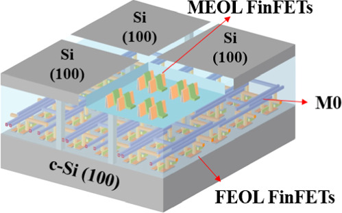
Fig. 1. Monolithic 3D MEOL Si single-crystal islands using the ELLPE technique.
Download figure:
Standard image High-resolution image2. Experimental methods
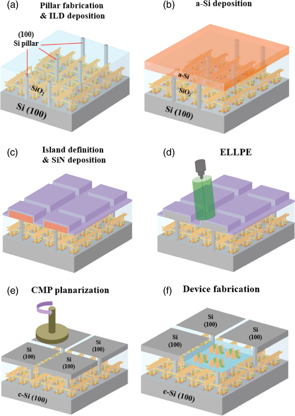
The process for fabricating the MEOL FinFET circuit is shown in Fig. 2, illustrating the crucial process steps involved in creating single-crystalline Si FinFETs through the ELLPE technique. First, single-crystal Si pillars, measuring 200 nm in diameter and 400 nm in height, were defined on the (100) Si wafer by using lithography and dry etching. Subsequently, a SiO2 layer was deposited and then thinned through chemical-mechanical polishing (CMP) to expose the Si pillar, as shown in Fig. 2(a). Following this step, the surface of the pillar was attentively cleaned using diluted hydrofluoric acid (at a ratio of 1:50) to eliminate the native oxide layer. Immediately thereafter, 150 nm thick amorphous silicon (a-Si) films were deposited using plasma-enhanced chemical vapor deposition at 375 °C.

Fig. 2. Process flow of MEOL Si FinFETs using low thermal budget ELLPE technique.
Download figure:
Standard image High-resolution imageThe following steps involved patterning the Si islands, capping them with a 10 nm thick silicon nitride layer to suppress spontaneous nucleation, and subjecting them to recrystallization via green nanosecond laser crystallization at 6.0 W, as shown in Fig. 2(c). The laser parameters included a wavelength of 532 nm, pulse width of 13 ns, frequency of 50 000 Hz, scan rate of 25 mm s−1, and beam size of 2190.6 × 42.2 μm2.
After Si crystallization, a SiO2 layer was deposited, followed by applying CMP process to planarize and reduce the thickness of the Si islands to approximately 50 nm, as depicted in Fig. 2(d), with the thickness increased to 100 nm for electron backscattering diffraction (EBSD) and transmission electron microscope (TEM) samples. Subsequently, the active region, comprising Si fins within the islands, was defined. The high-k/metal-gate process involved several steps. First, post-channel cleaning was performed. Next, a 5 nm thick HfO2 layer was deposited using plasma-enhanced atomic layer deposition. Then, multi-layer metals were deposited, including TaN (400 nm) and TiN (100 nm), through physical vapor deposition. Finally, lithography and etching processes were applied.
The creation of source and drain (S/D) regions involved boron and phosphorus implantation at a dose of 5 × 1015 cm−2, utilizing the energy of 10 keV, and tilt and twist angles of 7° and 22°, respectively. Subsequently, a 10 nm thick Ni film was deposited, and nickel silicide was formed through a two-stage rapid annealing process. This annealing process was conducted in a nitrogen (N2) environment, with temperatures set at 270 °C for 60 s followed by 400 °C for 30 s. The main purpose of this process was to mitigate the short-channel effects arising from the formation of shallow junctions at the source and drain regions. Finally, the fabrication of Si FinFETs was completed through the standard passivation and metallization processes.
3. Results and discussion
Figure 3(a) demonstrates the control of crystal orientation in the SCIs using a Si pillar on a (100) Si substrate and the ELLPE technique. During the short-pulse laser annealing, both the a-Si film and the tops of the Si pillars were melted, resulting in a liquid phase state. As the laser switched off, heat dissipated through the Si pillar, facilitated by its higher thermal conductivity, causing the molten Si to solidify. Subsequently, the liquid phase epitaxy process was initiated at the Si pillar and extended laterally towards the island's edge.

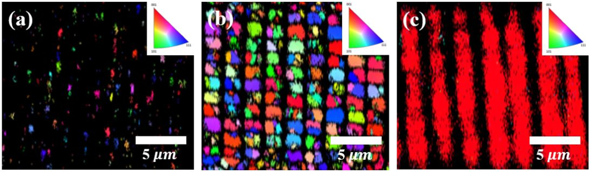
Fig. 3. (a) Schematics of ELLPE technique during green nanosecond pulse laser; (b) tile-view SEM image of Si single crystal island and its (c) EBSD mapping analysis.
Download figure:
Standard image High-resolution imageFigure 3(b) presents the SEM image of Si SCIs with dimensions of 1.3 μm × 1.3 μm, and their characterization is shown in Fig. 3(c) through EBSD mapping. In Fig. 3(c), it is evident that regions where the ELLPE technique was applied consistently exhibit a uniform (100) crystal orientation aligned with the Si pillar, while regions lacking the Si pillar maintain a morphology characterized by random grain boundary arrangements and varied crystal orientations. The presence of a uniform (100) crystal orientation matching that of the Si pillar is notably evident in the regions with a seeding structure.
In contrast, compared to ELLPE Si, the conventional poly-Si was recrystallized, employing a stacking arrangement composed of Si/SiO2/150 nm Si layers and green nanosecond laser crystallization at 6.0 W. The poly-Si films exhibit random grain boundaries and orientations, whereas the ELLPE single-crystal Si islands consistently display a uniform (100) orientation across their entire 1.3 μm × 1.3 μm surface areas. The ELLPE technique involves the full melting of the Si islands by the green nanosecond laser, with the single-crystal Si pillars serving as nucleation sites for Si crystal growth towards the edge of the islands. As a result, uniform (100) oriented single-crystal Si islands are achieved, aligning with the orientation of the Si pillar.
To examine the crystalline structure of the single-crystal Si islands obtained through the ELLPE technique, TEM analysis was conducted and the results are presented in Fig. 4. TEM cross-section images reveal well-arranged Si atoms, both at the junction between the Si pillar and SCI and along the edges of the SCI. Notably, the Si SCI doesn't exhibit observable grain boundaries or defects. Moreover, the material exhibits uniform single-crystal characteristics, both along its edges and at the corners, as confirmed by the presence of an identical selected area diffraction pattern.

Fig. 4. TEM cross-section images and selective area diffraction patterns of a Si single-crystal island.
Download figure:
Standard image High-resolution imageFollowing the verification of the single-crystalline nature of the Si islands, p-type and n-type Si FinFETs were further manufactured with a channel width of 30 nm and a gate length of 150 nm using the ELLPE technique. Comprehensive characterization was subsequently performed on these devices. Figures 5(a) and 5(b) show the transfer and output characteristics of ELLPE Si FinFETs, respectively. The electrical characteristics of both p-type and n-type Si FinFETs are presented in Fig. 5(a) through Id–Vg (drain current versus gate voltage) curves measured at Vd (drain voltage) values of 0.1 V and 1 V, as well as Id–Vd (drain current versus drain voltage) curves measured at Vg (gate voltage) of −0.2 V/step (ranging from 0 to 2 V).

Fig. 5. (a) Id/Vg curves of MEOL Si SCI FinFETs; (b) Id/Vd curves of a MEOL n-type Si SCI FinFET.
Download figure:
Standard image High-resolution imagePoly-Si semiconductor devices often have poorer performance compared to their monocrystalline silicon counterparts. 26–29) The main reason is the presence of grain boundaries and lattice defects in poly-Si, which restrict the movement of charge carriers. As a result, poly-Si devices tend to operate more slowly, consume more power, and exhibit greater variability in performance. In contrast, the uniform crystalline structure of monocrystalline Si enables better carrier mobility and superior electrical properties, making it the preferred choice for high-performance semiconductor devices. Therefore, this structure could be the preferred choice for high-performance semiconductor devices. Although poly-Si offers cost advantages, its inherent limitations make it less suitable for applications requiring top-tier performance.
For p-type Si FinFETs, the Ion/Ioff ratio is determined to be 1.5 × 10⁵. Specifically, at Vd = −0.1 V, the subthreshold swing (S.S.) is measured at 68 mV/decade, and the threshold voltage (Vth) is −0.23 V. At Vd = −1 V, the S.S. is observed to be 74 mV/decade, with a Vth of −0.26 V and ignorable drain-induced barrier lowering (DIBL). In the case of n-type Si FinFETs, the Ion/Ioff ratio is found to be 2.5 × 10⁵. At Vd = 0.1 V, the S.S. is measured at 76 mV/decade, and the Vth is 0.20 V. At Vd = 1 V, the S.S. remains at 74 mV/decade, with a Vth of 0.16 V.
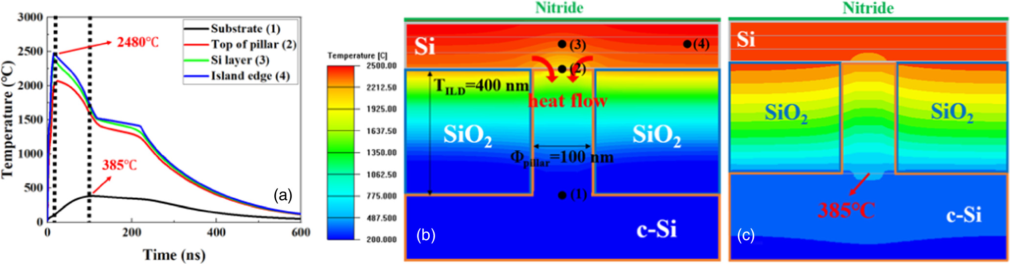
The application of computational fluid dynamics tools for thermal budget simulations is a fundamental and essential element in gaining a comprehensive understanding of the intricate behavior exhibited by MEOL FinFET circuits. In contrast to previous cases that relied on interlayer dielectric (ILD) for heat isolation, 30–32) silicon pillars are now employed as seeding structures to promote single-crystal orientation SCIs. It is crucial to recognize that a significant amount of heat can transfer through the Si pillar during the ELLPE process, highlighting the necessity for meticulous heat management. Therefore, implementing effective heat control measures becomes imperative to safeguard the integrity of the core FEOL circuits.
Figure 6(a) displays time-dependent temperature profiles recorded during the ELLPE process using a pulsed laser. During the laser operation (in the ON state), both the a-Si film and the top of the silicon pillar absorb laser energy within a mere 13 ns. Although high temperatures of 2562 °C and 2068 °C for the a-Si film and pillar top can be observed, the temperature remains remarkably low at just 97 °C at the bottom of the silicon pillar. During the OFF state, heat dissipation occurs through the silicon pillar and is conducted towards the lower silicon substrate, as depicted in Figs. 6(b) and 6(c). For a specific case with a 100 nm diameter pillar (Φpillar) and an ILD thickness (TILD) of 400 nm, the maximum temperature at the base of the silicon pillar reaches 385 °C within 109 ns. It is crucial to note that this temperature level aligns perfectly with the requirements of the BEOL process, which necessitates maintaining temperatures below 400 °C to ensure the structural and functional integrity of the underlying devices.

Fig. 6. (a) Time dependency of temperatures at the different positions during Si ELLPE; temperature distribution at the moments of (b) 24 ns and (c) 109 ns.
Download figure:
Standard image High-resolution imageBased on the findings from EBSD mapping analyzes, it is evident that an increase in laser intensity leads to a continuous enlargement in the grain size of recrystallized grains, as shown in Fig. 7. Once the laser intensity surpasses a particular threshold, the fabrication of SCIs with uniform crystal orientation is achieved.
Fig. 7. EBSD mapping analysis of ELLPE technique at different laser power densities: (a) 4.5 W; (b) 5.5 W; (c) 6.0 W.
Download figure:
Standard image High-resolution image
4. Conclusions
We have proposed the ELLPE technique, which has been demonstrated to effectively produce SCIs. These SCIs are subsequently used in the fabrication of MEOL FinFETs. The uniform (100) crystal orientation of each single crystal island was confirmed through TEM and EBSD analyzes. By adopting this low-thermal-budget method, we can successfully create channels in upper-layer devices while preserving the electronic characteristics of the underlying devices. Additionally, the consistent crystal orientation within the SCI region significantly mitigates device performance variability. These results underscore the potential of the ELLPE technique in enhancing the performance and reliability of advanced electronic devices in the realm of monolithic 3DIC.
Acknowledgments
This work was financially supported by the "Center for the advanced Semiconductor Technology Research" from The Featured Areas Research Center Program within the framework of the Higher Education Sprout Project by the Ministry of Education (MOE) in Taiwan. Also supported in part by the National Science and Technology Council, Taiwan, under Grant NSTC 112-2221-E-A49-163-MY3, and NSTC 110-2221-E-A49-086-MY3.