
Abstract
Many organisms have functional microstructured surfaces. Particularly, lotus leaves have hierarchical dual-scale micro/nanostructures on their surface and exhibit highly water repellent properties. We have developed techniques to fabricate patterns on inorganic material surfaces such as ceramics. Applying these techniques to fabricate hierarchical structures can make ceramic surfaces even more promising. In this paper, we prepared 2 kinds of mold with line-and-space patterns with pitches 50 μm and 2 μm and fabricated micro (rough patterns)/submicron (fine patterns) hierarchical structures on sintered ceramic sheets using a newly developed imprinting process with in-plain compression method. We proposed processes for the fabrication of such hierarchical structures, discussed the possibility of higher resolution of the patterns by comparison with the analytical results.
1. Introduction
In nature, there are many organisms with functional surface microstructures. One of the most famous examples is lotus leaves. Lotus leaves possess the hierarchical structures with dual-scale micro/nanostructures on their surface, and exhibit highly water-repellent properties. Many studies have been conducted on fabricating micropatterned surfaces that mimic such organisms in nature. 1–7) Some studies have also been conducted on the fabrication of lotus leaves-like hierarchical structures. 8–10) For ceramics, fabrication of microstructures using self-assembly has been studied, 11–13) but it is difficult to freely control the periods and shapes of the micropatterns. And a low-cost fabrication process for ceramics with dual-scale micro/nano scale hierarchical structures has not been developed. 14–19) Ceramics are one of the most promising materials in various fields due to their hardness, strength, heat resistance, corrosion resistance and chemical resistance, while ceramics are difficult to microfabricate.
To develop this process, we have focused on nanoimprint lithography (NIL), a microfabrication technique developed by Chou. 20–22) NIL is a low-cost and high-throughput technique for a variety of materials and is generally used for patterning resins. We have reported on the combination of NIL and powder metallurgy techniques to obtain finely patterned ceramic sheets, and named it "micro-powder-imprinting (μPI)." 23–29) Figure 1 shows a schematic diagram of the μPI process. First, ceramic nanopowders are mixed and dispersed with a polymer binder to prepare a compound sheet. The compound sheet is then imprinted using a mold in the same way as for NIL, and fine patterns are fabricated on the surface. After heating at high temperatures, the resin binder is removed and adjacent ceramic particles gradually bond to each other, resulting in smaller gaps between particles and overall shrinkage. Thus, a dense ceramic sheet is obtained. In our previous work, we fabricated submicron pitch line-and-space patterns on sintered ceramic sheets using ceramic powders with an average particle size of about 100 nm. 30) Hierarchical structures with submicron scale patterns on ceramic surfaces had not yet been realized using the imprinting method.

Fig. 1. Schematic diagrams of debinding and sintering in micro-powder imprinting.
Download figure:
Standard image High-resolution imageIn this paper, we propose a process to fabricate micro (rough patterns)/submicron (fine patterns) hierarchical structures on sintered ceramic sheets. Hierarchical structures with submicron patterns were achieved for the first time in this study. By in-plane compression of these hierarchical structures, changes in pitch, depth, and other characteristics were also investigated. Furthermore, the possibility of higher resolution of the patterns was discussed by comparison with the analytical results.
2. Multi-step imprint process
We have developed the 2-step imprinting process to fabricate hierarchical structures on ceramic surfaces. 31–33) Figure 2 shows 2-step imprinting process flow. This process uses fine and rough molds and compound sheets. First, the fine mold is imprinted to fabricate fine patterns [Fig. 2(i)]. Then, a protective resin layer is spin-coated onto the surface of the pattern [Fig. 2(ii)]. Next, rough mold is imprinted to fabricate rough-fine patterned hierarchical structures [Fig. 2(iii)]. A protective layer and resin in a compound sheet are removed by heating at high temperatures and ceramic particles are sintered, resulting in fabricated ceramics with hierarchical structures [Fig. 2(iv)]. This method has the advantage that the patterns to be fabricated can be determined by changing the pitch and depth of the mold patterns. Also, in contrast to general imprinting that uses only resin, it is possible to remove the protective layer resin at appropriate temperatures.

Fig. 2. Flow of the 2-step imprinting process. (i) 1st imprinting is carried out using a fine mold. (ii) A protective layer is applied by spin coating. (iii) 2nd imprinting is carried out with a rough mold. (iv) High-temperature heating removes resins and sinter ceramic particles.
Download figure:
Standard image High-resolution imageIn combining with 2-step imprinting, we have developed in-plane compression process to obtain higher aspect ratios of the imprinted structures. 31–34) Figure 3 shows in-plane compression process flow. This process uses a rubber substrate and an imprinted compound sheet before debinding. The compound sheet is bonded to a pre-tensioned rubber substrate and compressed by in-plane elastic recovery. As a result, the pitch of the patterns is smaller, and the aspect ratio of the structures can be increased. In this step, the fine patterns are deformed to be folded. In this study, we aim to fabricate micro/submicron hierarchical patterns on ceramic surfaces by combining these two processes.

Fig. 3. Flow of the in-plane compression process. (i) Elastic substrate is pre-tensioned. (ii) Imprinted sample is adhered onto the substrate. (iii) The sample is deformed in-plane with the elastic recovery of the substrate. (iv) High-temperature heating removes resins and sinter ceramic particles.
Download figure:
Standard image High-resolution image3. Materials and methods
In this paper, as the compound sheet materials, alumina powder (TM-DAR, Taimei Chemical Industry Co., Ltd.), polyvinyl alcohol (PVA; Wako Pure Chemical Industries, Ltd.), and glycerin (Wako Pure Chemical Industries, Ltd.) were used. The average particle size of the alumina powder was about 100 nm and its purity was 99.99%. PVA was used as a binder for the alumina powder. The degree of polymerization of PVA was 500 and its degree of saponification was 86.0–90.0 mol%. Glycerin was used as a plasticizer. The compound sheet consisted of alumina powder, PVA, and glycerin in a volume ratio 50:35:15. Figure 4 shows schematic flow of the process of making the compound sheet. First, the slurry was prepared by mixing with pure water [Fig. 4(i)]. Next, the slurry was spread on a PET sheet using the doctor blade method [Fig. 4(ii)]. The sheet was then dried at 70 °C for 0.9 ks to evaporate the water [Fig. 4(iii)]. Finally, the sheet was cut into 19.8 mm squares to fit into a container used for the following imprinting process [Fig. 4(iv)].

Fig. 4. Schematic flow of making the compound sheet. (i) Mixing sheet materials. (ii) Applying slurry on a film. (iii) Heating in an oven. (iv) Cutting into 20 mm.
Download figure:
Standard image High-resolution imageIn order to prevent the master patterns from being damaged the rigid alumina particles during imprinting, we transferred the patterns onto high-hardness RT-vulcanizing (RTV) rubber (KE-1600, Shin-Etsu Chemical), and used it as a mold. First, 10% curing agent (CAT-1600, Shin-Etsu Chemical) was mixed with KE-1600. The mixture was stirred, poured on the master pattern, and degassed to remove bubbles. After degassing, curing agent was filled into the patterns by centrifuging at 270 rpm for 600 s. The master pattern was then transferred to the RTV rubber by curing in an oven at 70 °C for 3.6 ks. The patterned RTV rubber mold was then further cured by heating in an oven at 150 °C for 1.8 ks, increasing the hardness from 45 to 70 on the Durometer Type A scale. The schematic of fine and rough patterns is shown in Fig. 5. The pitches of the respective line-and-space patterns were 2 μm and 50 μm. The RTV rubber mold was cut into 20 mm squares as well as the compound sheet.

Fig. 5. Micrographs and schematic diagrams of the cross-sectional patterns of the fine and rough molds. The fine pattern pitch and depth were 2 μm and 250 nm. The rough pattern pitch and depth were 50 μm and 50 μm.
Download figure:
Standard image High-resolution imageBefore 1st imprinting, the compound sheet was placed in a thermo-hygrostatic chamber at 30 °C and humidity of 80% for 1.8 ks to keep the water content constant. The compound sheet, the fine RTV rubber mold, and punches were then placed in a container as shown in Fig. 6 and pressed at 17.5 MPa for 60 s while heated to 100 °C. The container was used to prevent the compound sheet from flowing out horizontally. After being kept in the container until cooled to 40 °C, the protective layer, 2 mass% of Polyethylene oxide (ALKOX EP-10, Meisei Chemical Works), was spin-coated at 500 rpm for 10 s and dried in an oven at 60 °C for 900 s. The 2nd imprinting was also carried out under the same conditions as the 1st imprinting using the rough RTV rubber mold after water content of the compound sheet was kept.

Fig. 6. Images of the imprint equipment and diagram of the container, the molds, the compound sheet, and the punches.
Download figure:
Standard image High-resolution imageFor in-plane compression, first, the imprinted sample was placed in a thermo-hygrostatic chamber at 30 °C and humidity of 80% for 1.8 ks to keep the water content constant. Next, the imprinted sample was bonded to the pre-tensioned silicone rubber substrate (0.3 mm thick silicone sheet, AS ONE) using the adhesive (Arabic Yamato, YAMATO Co., Ltd.). After being placed in a chamber again at 30 °C and humidity of 90% for 1.8 ks, the load applied to the silicone rubber was released by changing the length of the substrate to the specified value. The sample was compressed by the elastic recovery force.
Figure 7 shows the heating program of sintering. The rate of temperature increase was 200 °C/3.6 ks and the sintering temperature was 1350 °C.

Fig. 7. Heating program of sintering.
Download figure:
Standard image High-resolution image4. Results and discussion
First, we describe the dimensional changes during the 1st and 2nd imprinting steps. Figure 8 shows cross-sectional SEM micrographs of the imprinted patterns of the samples. The ceramic surface layer was covered by the polymer protective layer so that the samples were kept at 600 °C for 1.8 ks to remove the polymer before observation. Figures 8(a)–8(c) show the sample after imprinting with the fine mold, after 2-step imprinting with the fine and rough molds, and after 2-step imprinting and sintering, respectively. Figure 8(d) shows an enlarged view of the microstructures depicted in Fig. 8(c). Sintering was conducted based on the conditions shown in Fig. 7. After the 1st imprinting, line-and-space patterns with a pitch of 2 μm were fabricated on the surface of the sample. The pattern was not very clear since the size of the primary particles ceramics was about 100 nm while the depth of the fine-mold pattern was 250 nm. This is discussed in our previous report. 30) The alumina particles are clearly observed. The surface of the sample after 2-step imprinting remained the fine patterns on the surface of the rough patterns fabricated by the rough mold. Also, fine patterns were obtained on the surfaces even after the alumina particles were sintered into dense ceramic sheets, fabricating micro/submicron scale hierarchical structures. Hierarchical structures with submicron patterns were achieved for the first time in this study.

Fig. 8. Cross-sectional SEM micrographs. (a) After imprinting with the fine mold and debinding (600 °C, 7.2 ks). (b) After 2-step imprinting with the fine and rough molds, and debinding. (c) After 2-step imprinting and sintering (1350 °C, 7.2 ks). (d) Enlarged view of the microstructures depicted in (c).
Download figure:
Standard image High-resolution imageWe focused on difference of the fine patterns observed on the peak areas of the rough patterns and on the valley areas. The patterns in the valley looked unclear. To discuss these results, we performed finite element simulation of the deformation during 2-step imprinting. For the analysis, we used the generalized Maxwell model for the finite element analysis. A commercial FEA software, ANSYS, was used for this simulation. The detailed simulation method was described in the reference. 33)
In this simulation, we employed cosine wave patterns for the rough mold and rectangular wave patterns for the fine mold. The pitches for each pattern were set at 140 μm and 10 μm, and the pattern depths of 65 μm and 10 μm, respectively. The simulated deformation during the 2nd-stage imprinting is shown in Fig. 9. From the top, the rough mold, the upper layer of the sheet shows the protective layer and the lower layer of the sheet shows the compound sheet after 1st imprinting. The protective layer and the compound sheet were bonded together to prevent detachment. From left to right in Fig. 9, the imprinting process was advanced by displacing the rough mold downwards. During the process, initial contact occurred between the peaks of the rough mold and the sheet. At these areas, the fine patterns in the regions experienced some elongation, resulting in larger pitch dimensions and shallower depths. Conversely, due to the minor deformation of the peak regions, the fine patterns remained intact without distortion. The variations in line width and depth at the valley to peak regions are plotted in Fig. 10. The line width in the valley region reached a maximum of approximately 11 μm during imprinting, representing an approximately twofold increase compared to the initial line width of 5 μm for the fine patterns. The line width of each pattern gradually decreased from the valley to peak regions, reaching a minimum of about 4 μm at the peaks. The depth in the valley region reached a maximum of approximately 5 μm, which was less than half of the pre-imprint depth. The depth exhibited almost linear increase from the valley to peak regions, reaching a maximum of approximately 14 μm at the peaks.

Fig. 9. Cross-sectional images during the rough mold imprinting in 2-step imprinting, obtained by the simulation.
Download figure:
Standard image High-resolution image
Fig. 10. The line width and the depth changes of the fine patterns during 2-step imprinting, obtained by simulation.
Download figure:
Standard image High-resolution imageThe similar tendency was observed in the experimental results, which suggest that the fine patterns in the valley regions became less distinct during imprinting due to their depths being reduced to less than half of those in the peak regions. Due to the utilization of relatively smaller mold patterns compared to particle sizes, the depth decreased in the valley areas, making pattern observation difficult.
In the current analysis, larger fine patterns were set for computational resource considerations. However, it is anticipated that the observed trend, as described above, remains consistent regardless of pattern size.
Next, the pattern changes by in-plane compression process are shown. Figures 11(a) and 11(b) show cross-sectional SEM micrographs of the sintered samples before and after the in-plane compression, respectively. The rough patterns fabricated through the 2nd imprinting process underwent horizontal compression, resulting in a pitch reduction of approximately 0.7 times. Furthermore, even after in-plane compression, a hierarchical structure with fine patterns on the surface was obtained. The pitch, depth, and half-width of the rough patterns were measured to quantitatively evaluate the deformation before and after in-plane compression. The half-width of the concave areas refers to the distance shown in Fig. 12. The measured values are summarized as shown in Fig. 13. Compared to before in-plane compression, the pitch shrank by about 32%, the depth by about 17% and the half-width of the concave areas by about 74%. The much larger shrinkage of the concave half-width compared to the pitch was due to the concave areas being compressed preferentially over the convex areas during in-plane compaction. The shrinkage of the depth was considered to be due to thinner protective layer thickness in the concave areas during the rough patterns imprinting and subsequent preferential compression of the concave areas by in-plane compression, resulting in the convex areas adhering to each other. Given the shrinkage rate of the half-width of the concave areas, it is considered necessary to fabricate rough patterns with larger half-widths to obtain fine patterns with large aspect ratios and clear in the concave areas. If the half-width of the concave area is larger, the deformation of the fine patterns during imprinting will be smaller, and the concave areas will shrink a lot during in-plane compression, which should result in clearer fine patterns.

Fig. 11. Cross-sectional SEM micrographs after sintering (1350 °C, 7.2 ks). (a) After 2-step imprinting. (b) After in-plane compression process.
Download figure:
Standard image High-resolution image
Fig. 12. Schematic diagram of the half-width in the valley region.
Download figure:
Standard image High-resolution image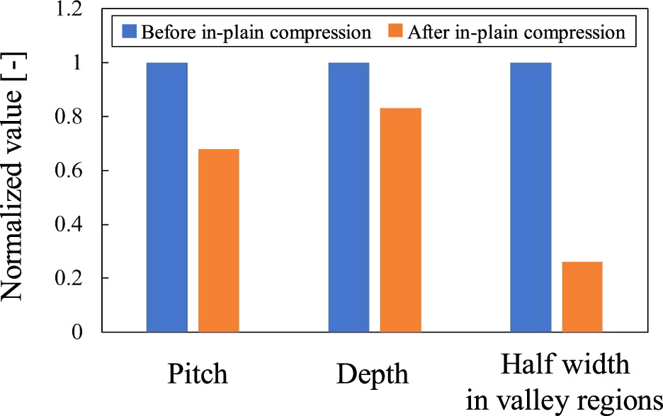
Fig. 13. The pattern pitch, the pattern depth, and the half width in the valley regions before and after in-plane compression. Normalized by the values before in-plane compression, respectively.
Download figure:
Standard image High-resolution image
5. Summary
In this study, we proposed 2-step imprinting and in-plane compression processes and fabricated hierarchical patterns with submicron scale patterns on ceramic surfaces after sintering. The fabricated patterns were compared with the FE-analysis results. By changing these parameters depending on the size of the fine patterns, clearer hierarchical patterns would be fabricated. Deformation at the bottom is crucial in this process, necessitating a more detailed evaluation. As observed in the analysis, the preparation of relatively deep fine molds would enable the quantitative evaluation of the obtained pattern pitch and depth. In the near future work, we plan to use fine patterns with deeper depths. The use of an analysis system also facilitates the design of hierarchical fine patterns. Additionally, it becomes feasible to apply this approach to surfaces mimicking the microstructures found in lotus leaves or morpho butterflies.
Acknowledgments
The SEM observation was made using JSM-IT700HR at the Center of Advanced Instrumental Analysis, Kyushu University.