
Abstract
We have investigated how the parameters of an input gate voltage (Vg) waveform and a drain voltage (Vd) impact the performance of reservoir computing (RC) using a Hf0.5Zr0.5O2 ferroelectric FET (FeFET). The RC performance is maximized by the high swing amplitude of the Vg and the most symmetrical polarization switching condition in the triangular-shaped input waveform, obtained by the center Vg of 0.5 V, because of the enhanced polarization switching of the FeFETs. Regarding the Vd dependence, the amount of the drain current and polarization switching have a trade-off relationship. As a result, a moderate Vd of 1.0 V becomes optimum in terms of the RC performance because a difference in drain current responses between different gate input patterns is maximized with this Vd. Furthermore, high computing capacities are achieved by combining the above optimal bias condition with drain current responses to both original and inverted gate input patterns.
Export citation and abstract BibTeX RIS
1. Introduction
The rapid development of information science technology has required versatile electrical hardware units and processing methods. Recently, machine-learning technologies based on deep neural networks have attracted significant attention. Here, low power consumption and low computational cost are highly emphasized to efficiently process huge volumes of information. However, the conventional Boolean logic and von-Neumann-computing architecture are inefficient in terms of power limitation and computational load, 1,2) which are particularly challenging for edge artificial intelligence (AI) processing. Accordingly, emerging electron devices such as 1D-nanostructure-based synaptic devices, two-terminal memristors, and multi-terminal synaptic transistors have been proposed for in-memory computing technologies. 3–5)
In the computing technology domain, reservoir computing (RC), which is one computational framework derived from recurrent-neural networks, is promising for temporal information processing. Figure 1(a) shows the schematic concept of an RC system which consists of three major components: an input layer, a reservoir part, and an output layer. The input layer is connected to the reservoir part with a fixed input weight so that time-series inputs are fed into the reservoir. The reservoir part has many history-dependent and nonlinear nodes that are randomly connected with each other through sparse-density recurrent connections having fixed weights. In the output layer, the readout part is connected to reservoir output nodes with adjustable readout weights that can be optimized by simple learning algorithms such as linear or ridge regression. 6,7) This computational cost is much lower than those of AI systems using backpropagation learning algorithms. Thus, RC systems are promising for real-time and low-power machine-learning applications. 8,9)
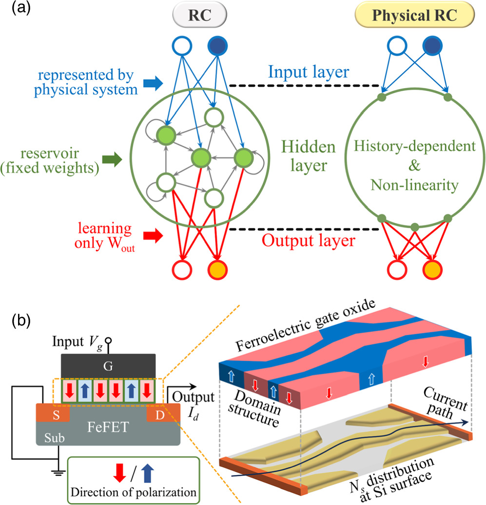
Fig. 1. (a) Concept of the RC system. (b) Schematic of FeFET with a dynamic ferroelectric polarization of gate oxide.
Download figure:
Standard image High-resolution imageThe reservoir in an RC system nonlinearly transforms time-series inputs into high-dimensional data to allow efficient training with a linear regression. To further improve the energy efficiency of AI computation toward edge AI, a physical RC in which the reservoir part is represented by a physical system has been proposed. 10) Effective physical reservoirs are required to have input-history dependence and nonlinear characteristics that transform the input data into a higher dimensional space. 11) Various RC systems utilizing a physical reservoir such as photonics, 12,13) spintronics, 14–16) electrochemical materials, 17,18) nanomaterials, 19–21) and memristors 22–24) have been proposed. Nevertheless, for practical edge AI computing implementation, further understanding of physical reservoir properties and on-chip integration technologies are highly required.
Our research group has demonstrated a physical RC system utilizing a Hf0.5Zr0.5O2 (HZO)-based ferroelectric FET (FeFET). 25–28) Hafnium oxide-based ferroelectric materials are promising as gate insulators of FeFETs because of the high compatibility with CMOS and scalability. 29–31) Here, the HZO-based FeFET is expected to transform time-series input signals into high-dimensional data through ferroelectric polarization, domain dynamics, and nonlinear interaction with channel carriers [Fig. 1(b)]. Therefore, HZO-based FeFET is promising as a physical reservoir for edge AI applications. We have reported the fundamental characteristics of the HZO FeFET-based RC system. 25,26) However, the impact of the bias conditions of FeFETs on the RC performance needs to be examined. Since the FeFET is fundamentally a multi-terminal device, optimization of the operating gate and drain bias conditions can enhance the RC performance.
In this study, we investigate how the parameters of input gate voltage waveform (Vg = v(t)) and drain bias voltage (Vd
) impact the performance of the HZO FeFET-based RC system. Moreover, we investigate the enhancement of the computational capacities by combining the optimum bias condition with an RC system utilizing complementary responses obtained by original ( ) and inverted gate input signals (
 ).
32) In addition to the published abstract,
33) we show new experimental data on the polarization switching currents of FeFETs and the RC performance with different values of Vd
. The correlation between the drain current (Id
) and the memory window of FeFETs with Vd
have been included to gain an understanding of the behavior of the RC performance. Furthermore, we analyze prediction rates for 16 different output patterns under input v(t) of "0110" and "1110" to gain insights into mistaken predictions. Finally, we deeply discuss the computing accuracy for 4-bit time-series inputs with different Vd
.
).
32) In addition to the published abstract,
33) we show new experimental data on the polarization switching currents of FeFETs and the RC performance with different values of Vd
. The correlation between the drain current (Id
) and the memory window of FeFETs with Vd
have been included to gain an understanding of the behavior of the RC performance. Furthermore, we analyze prediction rates for 16 different output patterns under input v(t) of "0110" and "1110" to gain insights into mistaken predictions. Finally, we deeply discuss the computing accuracy for 4-bit time-series inputs with different Vd
.
2. Experimental methods
The gate-last HZO FeFETs employed as the physical reservoir were fabricated as follows. We prepared (100)-orientated p-type silicon substrate with a doping concentration of 1015 cm−3. After a substrate cleaning process, a 210 nm thick SiO2 layer was thermally grown and patterned by a buffered-HF solution to define the active region. The highly-n-doped source and drain (S/D) regions were formed by ion implantation with P at 30 keV and followed by rapid-thermal annealing (RTA) at 1000 °C. Before gate stack deposition, the interfacial layer was chemically grown by a standard hydrogen peroxide mixture at 70 °C for 90 s to improve the MOS interface properties. 34) Then, an 11 nm thick HZO layer was deposited by atomic layer deposition at 300 °C using tetrakis(ethylmethylamino)hafnium (TEMAH), tetrakis(ethylmethylamino)zirconium (TEMAZ), and H2O as precursors. Subsequently, a 16 nm thick TiN metal gate was deposited by sputtering and annealed by RTA at 500 °C for 30 s in an N2 atmosphere to form the ferroelectric phase in the HZO layer. Finally, Al and silicon (2%)-doped Al were deposited as the gate and S/D contact electrodes, respectively, by thermal evaporation.
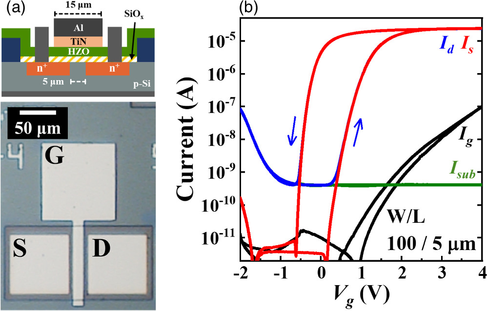
Figure 2(a) shows the schematic structure and an optical microscope image of a fabricated gate-last HZO FeFET with channel width and length of 100 μm and 5 μm, respectively. The channel length is defined by the separation of the highly-n-doped S/D region, which is not visible in the image. Figure 2(b) shows Id , source current (Is ), gate current (Ig ), and substrate current (Isub) of a HZO FeFET as a function of Vg . We can clearly confirm the ferroelectric (counterclockwise) hysteresis for Id and Is . Note that Ig increases at positive Vg is due to the leakage current from the gate to the channel through HZO, and that Isub increases at negative Vg is due to the gate-induced drain leakage (GIDL) current. 35)

Fig. 2. (a) Schematic structure and an optical microscope image of a fabricated gate-last HZO FeFET device. (b) Id , Is , Ig , and Isub of a HZO FeFET as a function of Vg with ferroelectric hysteresis.
Download figure:
Standard image High-resolution imageFigure 3 shows the schematic of a FeFET-based RC system utilizing the time response of Id (Id (t)) as virtual nodes and definitions of the pulse parameters. 10 sets of 1000 time-series random binary data u(n) (discrete time step n = 1, 2, ..., 1000) is encoded into a triangular-shaped waveform v(t) using a mask function with gate center voltage (Vg.center) and swing amplitude (Vg.sw). Here, the time period (tp ) of one triangular signal is 4 μs (0.25 MHz) and positive/negative swings correspond to 1/0 digital inputs. The Id (t) of a FeFET reservoir is sampled at 200 points per one period of input v(t) to obtain the virtual nodes x(i)(n) of the FeFET reservoir, where i (=1–200) is the virtual node number. In the output layer, after x(i)(n) is multiplied by each weight value, all the resultant values for i (=1–200) are summed to obtain the system output y(n). 25,36) In machine-learning computing, x(i)(n) values in the first 500 steps out of 1000 steps for each set are discarded to eliminate transient responses. Then, x(i)(n) values in the following 8 sets (4000 steps in total) are used in the training phase, where all the weight values are optimized for each specific task by ridge regression. The resultant weights and x(i)(n) values in the 2 sets (1000 steps in total) are used in the testing phase.

Fig. 3. Schematic of a FeFET-based RC system utilizing the time-response of Id as virtual nodes and definitions of the pulse parameters.
Download figure:
Standard image High-resolution imageGiven the delay time step Tdelay (=1–10), we perform two computational tasks 37,38) as the indexes of RC capacities of the HZO FeFET reservoir: short-term memory (STM; a capability to recall the input Tdelay steps back in the past) and parity check (PC; a capability to calculate if the number of 1 inputs during the recent Tdelay step is odd or even). Here, both short-term memory and nonlinearity can be evaluated for the PC task. The target signal d(n) for Tdelay is:


where ⊕ represents the XOR operator. In the testing phase, the computational capacity for each task is estimated by the squared correlation coefficient r2 between y(n) and d(n):
Here,  and
and  are the mean values of y(n) and d(n) over the n steps in the testing phase, respectively.
The capacities for the STM and PC tasks, CSTM and CPC are given by the sum of all r2 over the Tdelay step:

This summation is performed within the range of 1 ≤ Tdelay ≤ 10 because the r2 values fall to almost zero by Tdelay = 10.
3. Results and discussion
3.1. Center voltage optimization on RC performance
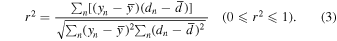
First, we examine the P-Vg characteristics of the fabricated FeFETs. Figure 4 shows the polarization switching current and the P-Vg hysteresis loop as a function of Vg.sw under different Vg.center conditions from −0.5 to 1.5 V (0.5 V step). The triangular-wave voltage with a frequency of 1 kHz is applied to the gate terminal and the displacement current of the HZO FeFET is measured. To evaluate the accurate P-Vg characteristics of the HZO FeFETs, the substrate and the S/D terminals are connected as illustrated in Fig. 4(a). The majority carriers from the substrate and minority carriers from the S/D regions ensure that the Si MOS surface is in equilibrium during fast-sweep-rate P-Vg measurements. 39) Figures 4(b) and 4(c) show that the two-polarization switching current peaks and the hysteresis loop increase with increasing Vg.sw . The most symmetrical polarization switching is obtained under Vg.center = 0.5 V because of the non-zero flat-band voltage of the FeFET. Then, the largest 2Pr value is achieved as shown in Fig. 4(d). On the other hand, when applying voltage waveforms to cause asymmetric polarization, only partial polarization switching in HZO occurs, resulting in a decreased 2Pr value.
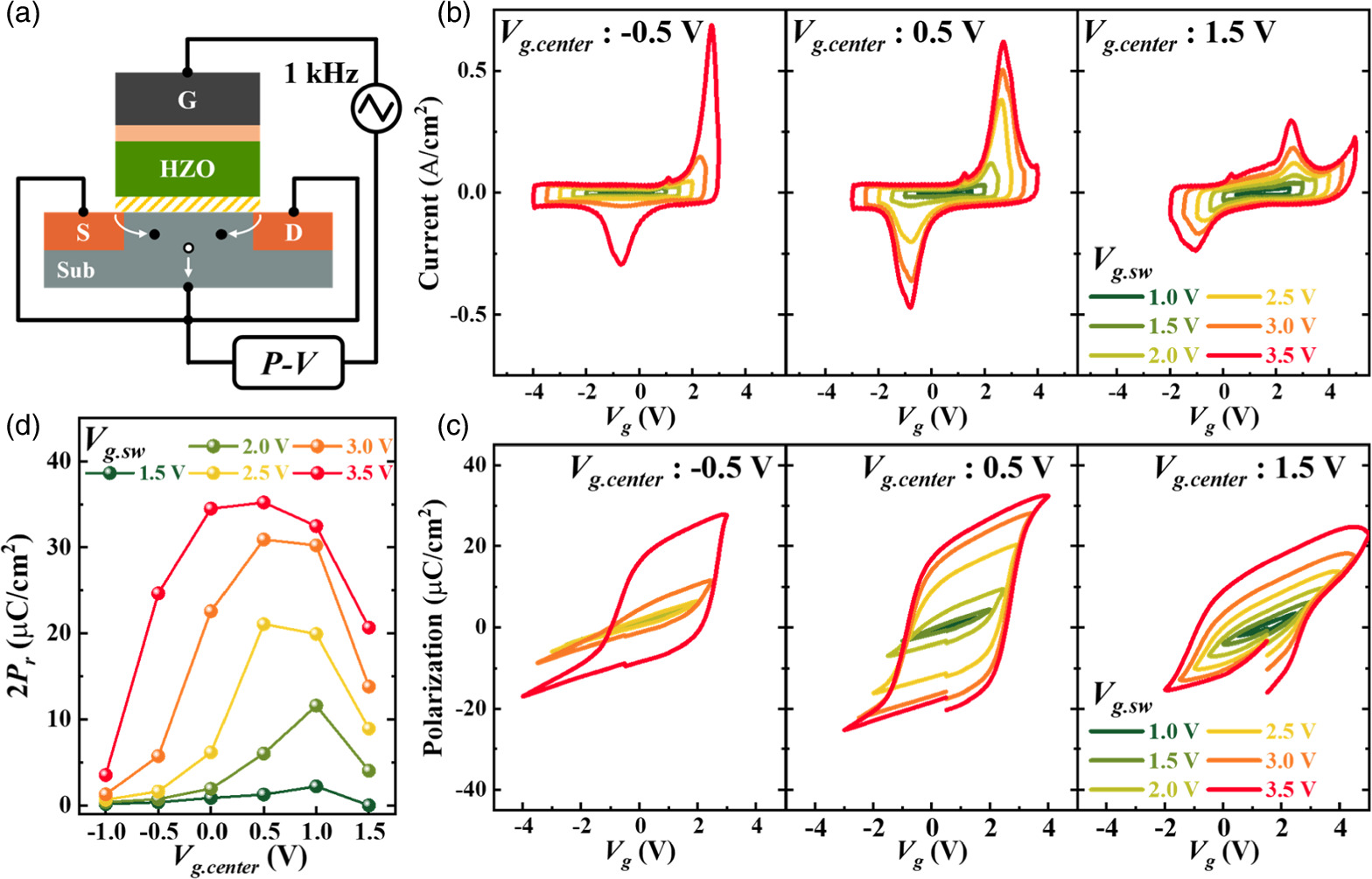
Fig. 4. Ferroelectric polarization switching properties of the fabricated HZO FeFET as a function of Vg.sw under different Vg.center conditions. (a) Schematic of the measurement circuit. (b) Polarization switching current, (c) P-Vg hysteresis loop, and (d) 2Pr values.
Download figure:
Standard image High-resolution imageFigure 5(a) shows the r2 values of the STM and PC tasks as a function of Tdelay with different Vg.sw conditions (Vd = 0.3 V). It is found that the HZO FeFET exhibits the computing performance for both STM and PC tasks up to Tdelay of 3, and that the r2 values at Tdelay = 2 are remarkably affected by Vg.sw . Figure 5(b) shows the comparison between y(n) and d(n) at Tdelay = 2 at two Vg.sw conditions. When a larger Vg.sw is used to generate the voltage input v(t), the agreement between the target d(n) and the computed output y(n) is improved in comparison with a smaller Vg.sw . As a result, the higher Vg.sw enhances the computing performance, which is attributable to the increased polarization switching. Figure 6 shows the computing capacities for STM and PC tasks with different Vg.sw as a function of Vg.center. The highest RC capacities are achieved under Vg.center of 0.5 V and Vg.sw = 4 V, attributed to the highly symmetric ferroelectric polarization switching. These results well match with those of the 2Pr analysis shown in Fig. 4(d).

Fig. 5. (a) r2 values of the STM and PC tasks as a function of Tdelay with different Vg.sw conditions (Vd = 0.3 V). (b) Comparison between y(n) and d(n) at Tdelay = 2.
Download figure:
Standard image High-resolution image
Fig. 6. Computing capacities for STM and PC tasks with different Vg.sw as a function of Vg.center.
Download figure:
Standard image High-resolution image3.2. Drain voltage optimization on RC performance
Next, we examine the impact of Vd
on the RC performance in order to find the optimum Vd
value in terms of the RC performance. Figure 7 shows the ferroelectric characteristics of a FeFET with various Vd
conditions. Figure 7(a) shows the P-Vg
characteristics and polarization switching current of the FeFET during the P-Vg
measurements with different Vd
conditions ( ≥ 0). As the Vd
increases, the potential difference between gate-to-source voltage (Vgs) and gate-to-drain voltage (Vgd) becomes more evident. When Vg
is swept in (I) and (II) regions shown in Fig. 7(a), the direction of polarization in HZO starts to be turned downward (Pdown). Here, when Vd
is applied, the polarization switching in HZO near the drain region is suppressed because Vgd is insufficient. When Vgd is sufficiently large, the drain-side domains also switch downward. As a result, as Vd
increases, the peak of the current associated with polarization switching decreases and shifts toward a larger Vg regime. When Vg
is swept in (III) and (IV) regions, Vgd becomes negative first compared to Vgs. Thus, the direction of polarization in HZO is driven upward (Pup) near the drain region first, followed by polarization switching near the source region. As Vd
increases, the peak of the switching current moves toward a smaller |Vg| regime. Figure 7(b) shows the P-Vg
hysteresis loop of the FeFET with different Vd
. We can confirm that the 2Pr
values decrease with increasing Vd
. This is because the reduced Vgd is insufficient to modulate the polarization condition in HZO near the drain region and decreases the total amount of polarization switching domains in the channel.
40,41)
≥ 0). As the Vd
increases, the potential difference between gate-to-source voltage (Vgs) and gate-to-drain voltage (Vgd) becomes more evident. When Vg
is swept in (I) and (II) regions shown in Fig. 7(a), the direction of polarization in HZO starts to be turned downward (Pdown). Here, when Vd
is applied, the polarization switching in HZO near the drain region is suppressed because Vgd is insufficient. When Vgd is sufficiently large, the drain-side domains also switch downward. As a result, as Vd
increases, the peak of the current associated with polarization switching decreases and shifts toward a larger Vg regime. When Vg
is swept in (III) and (IV) regions, Vgd becomes negative first compared to Vgs. Thus, the direction of polarization in HZO is driven upward (Pup) near the drain region first, followed by polarization switching near the source region. As Vd
increases, the peak of the switching current moves toward a smaller |Vg| regime. Figure 7(b) shows the P-Vg
hysteresis loop of the FeFET with different Vd
. We can confirm that the 2Pr
values decrease with increasing Vd
. This is because the reduced Vgd is insufficient to modulate the polarization condition in HZO near the drain region and decreases the total amount of polarization switching domains in the channel.
40,41)
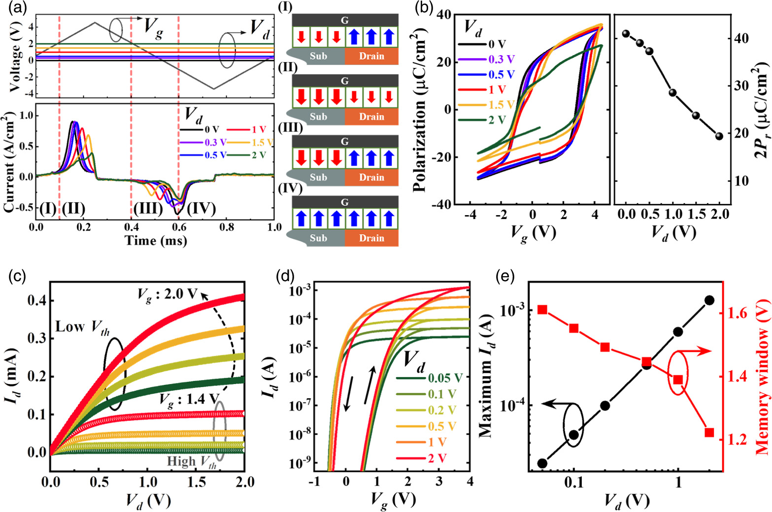
Fig. 7. Ferroelectric characteristics of a FeFET with various Vd conditions. (a) Polarization switching current, (b) P-Vg hysteresis loop, and 2Pr values with various Vd conditions. (c) Id –Vd characteristics with high/low Vth conditions. (d) Id –Vg characteristics, (e) maximum Id , and the memory window as a function of Vd .
Download figure:
Standard image High-resolution imageFigure 7(c) shows the Id –Vd characteristics for the FeFET with high threshold voltage (Vth) (−Ps initialization) and low Vth (+Ps initialization). The device operates in the linear region at small Vd and transitions into the saturation region with increasing Vd . When Vd exceeds the saturation voltage determined by Vg and Vd , the pinch-off occurs. Figure 7(d) shows the Id –Vg characteristics of the FeFET. It is observed that the memory window slightly decreases with an increase in Vd . Figure 7(e) shows the maximum Id values at Vg = 4 V and the memory window as a function of Vd . As Vd increases, the maximum Id increases by the higher lateral electric field, while the memory window decreases because of less switchable polarization at the drain side [see Figs. 7(a)–7(b)], indicating a trade-off relationship between Id and the memory window in terms of Vd . This decrease in the memory window is attributable to the decrease in 2Pr , shown in Fig. 7(b). Thus, this trade-off relationship between the increase in Id and the decrease in the amount of polarization switching can lead to the existence of the optimum Vd .
Figure 8 shows the computing capacities for STM and PC tasks under different Vg.center and Vg.sw conditions as a function of Vd . It is found that the computing capacities initially increase with increasing Vd , take a peak, and then decrease. The peak capacities are obtained at Vd = 1 V with Vg.sw of 4.0 V and symmetric Vg.center of 0.5 V.

Fig. 8. Computing capacities for STM and PC tasks under different Vg.center and Vg.sw conditions as a function of Vd .
Download figure:
Standard image High-resolution imageFigure 9(a) shows the r2 values of the STM and PC tasks with different Vd as a function of Tdelay. The meaningful computing performance is obtained up to Tdelay of 4 for STM and up to Tdelay of 3 for PC tasks. It is also observed that the r2 values at Tdelay of 3 are remarkably affected by Vd and significantly improved at optimal Vd . The r2 values in the 3-step-delay tasks mean the correlation between output y(n) and target d(n) by using the virtual nodes at u(n) to recall u(n-3). Meanwhile, 10 sets of 1000 time-series random binary data u(n) were used as input to the FeFET reservoir, various cases of 4-bit input patterns can be grouped and divided from the long random pattern, as shown in Fig. 9(c). In total 16 input patterns from "0000" to "1111," the left 3 bits in the 4-bit patterns mean the past history u(n-3), u(n-2), u(n-1) (leftmost bit means the input at Tdelay of 3) and the rightmost 1 bit means the present input u(n). To gain more understanding of the improvement of r2 at Tdelay of 3, we evaluated each accuracy of 3-step-delay tasks by separating the different input history and analyzed which input pattern is improved by Vd optimizing. In Fig. 9(b), the significant Vd dependence of the accuracy is observed for the "0110" input for both STM and PC tasks. It is found that the accuracy for the "0110" input is significantly improved by choosing the optimum Vd of 1.0 V.

Fig. 9. (a) r2 values of the STM and PC tasks with different Vd as a function of Tdelay. (b) Computing accuracy at Tdelay = 3 for 4-bit time-sequence inputs with a different history from "0000" to "1111" with different Vd conditions. (c) Schematic of procedure to extract 4-bit input patterns out of random input series.
Download figure:
Standard image High-resolution imageHere, when the accuracy at Tdelay of 3 is low, we can expect that "0110" can be misinterpreted as "1110" in high probability. In order to confirm this expectation, the probability distribution of prediction is evaluated for input of "0110" and "1110." The results are shown in Fig. 10. As expected, "0110" and "1110" are likely to be incorrectly predicted at Tdelay of 3 as "1110" and "0110," respectively. This fact indicates that the appropriate choice of Vd can typically enhance the prediction rate between "1110" and "0110." As a result, Vd of 1 V leads to the highest prediction accuracy of >83% with the lowest classification error rate of <17% for input v(t) of "0110," as seen in Fig. 10.

Fig. 10. Prediction rates of 16 different output patterns for input v(t) of "0110" and "1110".
Download figure:
Standard image High-resolution imageThus, in order to understand the physical origin of the reason why Vd of 1 V is optimum, the output Id waveform patterns for the input v(t) of "0110" and "1110" are examined. First, Fig. 11 shows the history-dependent Id (t) responses for "0110" with different Vd . It is observed that the Id (t) responses contain two distinct peaks, which can be due to the polarization switching current and the GIDL current. Here, the GIDL current increases with increasing Vd , whereas the polarization switching currents have the maximum at Vd of 1 V. The decrease in the polarization current with Vd higher than 1 V is attributable to the decrease in polarization switching domains in HZO near the drain region.
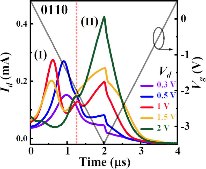
Fig. 11. History-dependent Id (t) responses for input v(t) of "0110".
Download figure:
Standard image High-resolution imageIn order to verify this interpretation, the difference in the history-dependent Id (t) responses between v(t) of "0110" and "1110" is compared. Figures 12(a)–12(e) show the Id (t) responses for v(t) of "0110" and "1110," and ΔId (t) between "0110" and "1110" with different Vd . The values of ΔId (t) are large in a short time region (t < 1.2 μs), where the polarization switching is dominant, and become smaller at longer times (t > 1.2 μs). This fact suggests that the current associated with polarization switching can contribute to the computing capabilities, because a large difference in history-dependent Id (t) responses is advantageous for identifying the input patterns. Figure 12(f) shows the maximum |ΔId (t)| in the polarization switching region (t < 1.2 μs) as a function of Vd . It is found that the largest |ΔId (t)| is obtained at Vd of 1 V, which results in the maximum RC performance at Vd of 1 V. Here, the largest |ΔId (t)| at Vd of 1 V can be explained by the trade-off relationship in the polarization switching current between Id and the amount of polarization switching domains, as shown in Fig. 7.
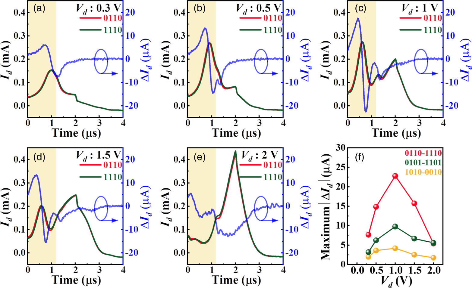
Fig. 12. (a)–(e) History-dependent Id (t) responses for v(t) of "0110" and "1110," and ΔId (t) between "0110" and "1110" with different Vd . (f) Maximum |ΔId (t)| in the polarization switching region (t < 1.2 μs) as a function of Vd .
Download figure:
Standard image High-resolution image3.3. RC performance improvement by complementary responses
Our group has previously reported that the RC capabilities in a single n-channel HZO FeFET reservoir are limited by the low current at negative input Vg
.
31,42) This is because sufficient information cannot be extracted from the low channel currents with Vg
lower than Vth. Therefore, a new computing scheme utilizing complementary information through original  and inverted
  as input signals has been proposed in the previous study.
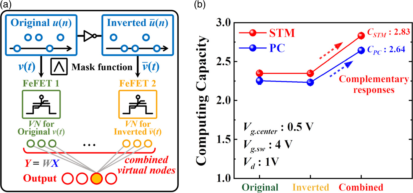
31) Thus, we also estimate the RC capabilities for this RC scheme utilizing complementary information under the optimized bias conditions, obtained in the present study. Figure 13(a) shows the schematic of the RC system utilizing complementary responses by
as input signals has been proposed in the previous study.
31) Thus, we also estimate the RC capabilities for this RC scheme utilizing complementary information under the optimized bias conditions, obtained in the present study. Figure 13(a) shows the schematic of the RC system utilizing complementary responses by  and
and  as input signals. Here, the inverted input signal
  is the waveform created by the logically inverted data of digital input
  The virtual nodes for RC computing are prepared by combining the Id
(t) values of the FeFETs in response to
The virtual nodes for RC computing are prepared by combining the Id
(t) values of the FeFETs in response to  and
and  Figure 13(b) shows the RC capacities for STM and PC tasks using the combined virtual nodes under the optimized bias conditions, Vg.center of 0.5 V, Vg.sw of 4 V, and Vd
of 1 V. There is no significant difference in the capacities between RC using the virtual nodes for the original input
Figure 13(b) shows the RC capacities for STM and PC tasks using the combined virtual nodes under the optimized bias conditions, Vg.center of 0.5 V, Vg.sw of 4 V, and Vd
of 1 V. There is no significant difference in the capacities between RC using the virtual nodes for the original input  only and those for the logically inverted input
  only. On the other hand, the computing capacities by using the combined virtual nodes are significantly improved. This is because the combined virtual nodes can include the components of high channel currents under the complementary gate voltages, irrespective of the positive and negative original input voltage, leading to rich information and resulting high computing capacities. As a result, the highest RC performance with CSTM = 2.83 and CPC = 2.64 is achieved under the optimized bias conditions.
Fig. 13. (a) Schematic of the RC system utilizing complementary responses by  and
and  as input signals. (b) RC capacities for STM and PC tasks using the combined virtual nodes under the optimized bias conditions (Vg.center of 0.5 V, Vg.sw of 4 V, and Vd
of 1 V).
as input signals. (b) RC capacities for STM and PC tasks using the combined virtual nodes under the optimized bias conditions (Vg.center of 0.5 V, Vg.sw of 4 V, and Vd
of 1 V).
Download figure:
Standard image High-resolution image
4. Conclusions
We have experimentally verified how the parameters of input v(t) and Vd conditions impact the HZO FeFET-based RC system and have optimized the operating voltage conditions to maximize the RC performance. For the gate voltage waveform, a high swing amplitude of 4.0 V and a center voltage of 0.5 V, which introduces the most symmetrical polarization switching, maximize the RC performance because of the high polarization switching current of FeFETs. Regarding the Vd dependence, it is necessary to consider the trade-off relationship between the increase in Id and the decrease in the amount of polarization reversal near the drain edge. As a result, a moderate Vd value of 1.0 V has been found to maximize RC performance by increasing the polarization current and the input history difference in the Id time response. Furthermore, the high computing performance with CSTM = 2.83 and CPC = 2.64 have been achieved in RC by combining the time-responses of Id to the original and inverted gate inputs of FeFETs under the optimal bias conditions, obtained in this study.
Acknowledgments
This work was supported by JST CREST (JPMJCR20C3) and JSPS KAKENHI (21H01359), Japan.