
Abstract
The degree of anisotropy and the domain arrangement of crystal structures in ferroelectrics are affected by the grain boundaries and by the shape and size of the grains. To understand the grain boundary effects that occur in ferroelectric ceramics, we introduce a technique for nondestructively observing the internal lattice strain distribution of a submicrometer-sized ferroelectric grain in polycrystalline materials. The ferroelectric phase transition of a single grain in the polycrystalline materials was evaluated by tracking the changes in the Bragg coherent X-ray diffraction (CXD) patterns. The internal lattice strain distribution of the grains in the paraelectric phase was visualized via Bragg CXD imaging. A pair of 90° domains in the ferroelectric phase were also imaged in three dimensions, and showed a domain boundary correlated with the internal lattice strain caused by the stresses from the adjacent grains.
Export citation and abstract BibTeX RIS
1. Introduction
Ferroelectrics with specific crystalline sizes exhibit dielectric properties and a degree of anisotropy, which depend on the crystalline sizes and shapes. 1,2) Barium titanate (BaTiO3, BTO), a typical ferroelectric material, shows a remarkable size effect where the crystalline sizes are in the range of several hundred nanometers (called mesoscale hereafter); 3–5) the tetragonality of BTO (c/a ratio) decreases monotonically when the particle size is less than 100 nm for isolated particles 6–8) and is less than 1 μm for polycrystalline ceramics. 4,9,10)
Anomalously high dielectric constants occur for particle or grain sizes at which the tetragonality begins to decrease. 4,6,10) The spontaneous electric polarization of ferroelectrics reduces with the decreasing tetragonality and disappears at a critical size. 2,11) The reported critical size values of BTO are 40, 7) 10–30, 9) 26, 12) and 8 nm, 13) and this variation in the critical size can be attributed to the shape of the crystals. 13) Thus, the crystalline sizes and shapes at the mesoscale significantly affect the ferroelectric and dielectric properties.
The size effect for polycrystalline ceramics used in dielectric and piezoelectric devices is more complicated than that for single-crystalline particles owing to the interactions between one crystalline grain and its surroundings. 14) A crystalline grain in a polycrystalline ceramic is subjected to stress and pressure from the adjacent grains. 5) The stress and pressure increase or decrease the number of 90° domain walls per unit cell volume in the crystal, resulting in anomalously high dielectric constants. 4) The anisotropic strain in the crystal lattice due to stress reduces the domain wall density, 15) whereas an isotropic pressure promotes the development of the paraelectric phase below Curie temperature. 16) These observations related to grain sizes, grain shapes, and internal lattice strain distributions will significantly aid in understanding the ferroelectricity of polycrystalline ceramics with size effects.
These aforementioned factors can be evaluated by nondestructively examining the mesoscale structure of a single grain in polycrystalline materials. The Bragg reflections from a single grain are distinguishable from those of the others, because grains with the same orientation are rarely adjacent to each other in polycrystalline ceramics. The ferroelectric domain inside a grain can be identified by measuring the Bragg reflections that characterize anisotropy; in the case of 90° domains of tetragonal BTO, pairs of 200/002 and 110/101 reflections appear. 3,17) Using X-rays with spatial coherence lengths in the micrometer scale (coherent X-rays hereafter) as probes, the grain sizes, shapes, and internal lattice strain distributions in a crystalline material can be determined. 18–20) Coherent X-rays are generated by third and later-generation synchrotron radiation sources, such as SPring-8. When coherent X-rays completely irradiate a crystalline particle or grain, a diffraction pattern—speckle 21)—forms, which contains information on the external shape, size, and atomic misalignment of the crystal (for Bragg condition). By analyzing an adequately sampled speckle pattern to retrieve the phase of the crystal structure factor, we can simultaneously image the shape, size, and lattice strain distributions of the structure that satisfies the Bragg conditions; 22,23) this technique is called Bragg coherent X-ray diffraction (CXD) imaging (Bragg-CDI). Bragg-CDI can be applied to speckles from a single grain buried in a polycrystalline ceramic to reconstruct a grain boundary with a lattice strain distribution, including ferroelectric domains.
In this study, considering the restrictions of the Bragg-CDI technique, we focused on the lattice strain distribution and outer shape of a BTO crystalline grain in the paraelectric (cubic) phase, and complemented these results with the temperature dependence of the CXD pattern and domain configuration in the ferroelectric (tetragonal) phase. The present Bragg-CDI technique cannot extract complete information on the shape and arrangement of ferroelectric domains from two (or more) separated Bragg peaks. Because the Bragg-CDI technique can be apply to only one Bragg reflection, for typical ferroelectric crystals with sufficient anisotropy (e.g. c/a ≥ 1 for tetragonal structures), the outer shape obtained from the reflection is not that of the whole crystal, but only that of the domain corresponding to that reflection. 24,25) Structure factor reconstructed by a computer-aided phase retrieval analysis of Bragg-CDI contains information on both domain boundaries and dislocations. 26) Moreover, for polycrystalline samples, the reconstructed image includes the intracrystalline grain boundaries. 20) In this study, we applied Bragg-CDI to a whole BTO single grain in the cubic phase and to 90° domains within the grain in the tetragonal phase to distinguish the domain boundaries, grain boundaries, and defects. For the tetragonal phase, domain boundary identification was performed by applying Bragg-CDI to each Bragg reflection corresponding to a pair of mutually adjacent domains. To augment the results obtained with Bragg-CDI, we also recorded the CXD patterns of the BTO grains in the cubic and tetragonal phases, including those near the ferroelectric phase transition temperature, using the same procedures previously reported for an isolated BTO particle. 27)
2. Experimental
2.1. Sample characterization
We prepared a BTO polycrystalline powder by grinding a BTO ceramic pellet in a mortar. The ceramic pellet was prepared by sintering a typical fine BTO powder synthesized by the hydrothermal method. We first used a large Debye-Scherrer camera with a multi-MYTHEN-detector system installed at the SPring-8 beamline BL02B2 28) to characterize the basic structure of the BTO polycrystalline powders. Temperature sweep measurements at approximately 0.4 K s−1 during heating were performed to assess the tetragonal-to-cubic phase transition in the BTO polycrystalline ceramics. To measure the temperature dependence of the crystal structure, the BTO polycrystalline powder was sealed in a borosilicate glass capillary with a 0.1 mm diameter. A high-temperature N2 gas flow system was used to change the sample temperature, which was maintained within 0.1 K. The temperatures of the powder samples were measured using a thermocouple device (K-type). The X-ray energy was 15.9 keV (λ = 0.78 Å), which was monochromatized by a Si(111) double-crystal monochromator (DCM).
The polycrystalline ceramics were sufficiently sintered from the starting material, i.e. the fine powder, and therefore, the powder diffraction patterns of the BTO polycrystalline ceramics exhibited a typical tetragonal-to-cubic phase transition. Figure 1 shows a two-dimensional (2D) intensity map, as a function of temperature, created using the diffraction patterns collected every 5 K (14 s exposure time, 0.2 s readout time, and 0.8 s waiting time). Upon heating, the 200T and 002T peaks approach each other and eventually merge to form a single 200C peak. Similar to the spectra of a bulk crystal, a steep peak splitting occurs at approximately 403 K (Curie temperature TC) in the spectra of the BTO polycrystalline ceramics, and this feature indicates the occurrence of the first-order phase transition.
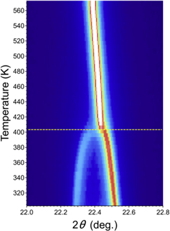
Fig. 1. Temperature dependence of the powder diffraction patterns of the BTO 200/002 reflections. The dashed-yellow line indicates the TC of the BTO polycrystalline powder (∼403 K).
Download figure:
Standard image High-resolution image2.2. Sample preparation
The following procedure was employed to prepare the sample for the CXD and Bragg-CDI measurements: (i) we ground the BTO ceramics pellet in a mortar [left of Fig. 2(a)] and dispersed (suspended) the clusters of BTO polycrystalline ceramics in ethanol using an ultrasonic apparatus; (ii) we transferred and dispersed them on a MEMS heating chip (Norcada Inc., HTN-0101H) using a high-precision spin coater (ACE-200, HiSOL, Inc.); (iii) we evaporated the ethanol in a vacuum chamber for several minutes. We used an MEMS heating chip with a 30–50 nm thick laminated membrane, in which spiral-patterned (Au) heating elements were sandwiched between crystalline SiNx membranes. 29) The heating chip also had 19 dents, each with a diameter of 3 μm, in the center, and these dents trapped and stabilized the BTO polycrystalline clusters as shown in the optical microscopy (VHX7000, Keyence Corp.) image in Fig. 2(a) (middle). The coherent X-rays were focused on one dent. As shown on the right side of Fig. 2(a), the CXD and Bragg-CDI measurements can detect only a single grain with an orientation satisfying the Bragg condition.

Fig. 2. (a) Sample preparation procedure for the CXD and Bragg-CDI measurements. (b) Schematic of the setup used for Bragg-CDI.
Download figure:
Standard image High-resolution imageThe prepared MEMS heating chip was mounted on a heating holder (Norcada Inc., NHB5100). 29) The temperature of the polycrystalline sample was determined by the resistance of the heating elements measured by four-terminal sensing; the terminals are shown in Fig. 2(b). For these measurements, the temperature was maintained between 303 K (30 °C) and 573 K (300 °C) within ±1 K. The measured temperature tolerances and drift velocities were similar to those reported in previous studies. 27,29)
2.3. CXD measurements
The CXD and Bragg-CDI experiments were carried out using the CDI instruments 26,27,30) installed at the BL22XU beamline in SPring-8. 31)
Liquid-nitrogen-cooled Si(111) DCM-monochromatized X-rays, with energy tuned to 8 keV (λ = 1.5498 Å), were obtained from an in-vacuum undulator. The heating holder was mounted on a vacuum chamber, 26,27) and the mounting holder was compatible with the other membrane holders. 26) The X-rays were focused using a refractive lens (Karlsruhe Institute of Technology 32)) with a typical size of 2.9(6) × 2.00(3) (vertical × horizontal) μm2 and a focal length of 1.0 m. The sample indicated by the white arrow in Fig. 2(a) was illuminated using these focused X-rays. The MEMS heating chip did not affect the X-ray coherency.
As shown in Fig. 2(b), the diffracted X-rays were detected in three dimensions using a 2D photon-counting detector (Eiger500k, Paul Scherrer Institute), around the Bragg position, by changing the Bragg angle (ω scan, while 2θ and χ were fixed) by ±1.2°. The pixel size of the detector was 75 × 75 μm2, and it was located at a position 0.7 m downstream from the sample. The 200 Bragg reflection was chosen for the current measurements with a scattering angle (2θ) of approximately 45.76°. An ac peak split associated with the tetragonal-to-cubic phase transition was expected if a domain structure formed inside the grain, as shown in Fig. 1. The above experimental settings meet the conditions required for phase retrieval of the observed CXD patterns, as indicated in Ref. 30.
This study was focused on the analysis of the CXD pattern changes and Bragg-CDI images of a BTO single grain in a polycrystalline cluster. We began the measurements using the tetragonal phase at 313 K. The temperature dependence of the CXD patterns was measured every 10 K from 313 to 573 K. The Bragg-CDI data were acquired at 313 and 573 K, which are the typical temperatures in the tetragonal and cubic phases, respectively. A series of hybrid input–output and error reduction algorithms, 33) commonly used in CDI, was used to retrieve the phase of the observed diffraction patterns. The shrink-wrap algorithm 34) was used to update the real-space constraints.
In this study, 2D speckle patterns and 3D images (including cross-sectional images) were drawn using ImageJ 35) and VESTA 3 36) respectively.
3. Results and discussion
The temperature-dependent CXD patterns of the ferroelectric single grain indicated the occurrence of a structural phase transition. Figure 3 shows the speckle patterns of the 200/002 Bragg reflections from a single grain in the BTO polycrystalline cluster at 313–573 K. The horizontal and vertical axes are 2θ and χ, respectively, and the scattering intensities are plotted on a logarithmic scale. We determined TC from the powder diffraction patterns shown in Fig. 1; the red arrow represents the scattering vector Q . In the tetragonal phase (T < TC), the Bragg spots split into two 200T and one 002T reflection peaks; the 200T reflections contain intense and weak spots (200T1 and 200T2, respectively). The 002T spots are connected to the 200T1 and 200T2 spots with their respective streaks. The 200T1-002T-200T2 connection corresponds to the 200T1-002T-200T2 domain configurations with mutually independent boundaries, as shown at the top left in Fig. 3. Considering the intensities of these spots, the volume of the 200T2 domain is significantly smaller than those of the 200T1 and 002T domains. The distance between the two spots decreases in the reciprocal space as the temperature is increased from 313 to 403 K, indicating that the tetragonality c/a decreases. Moreover, the intensity of the streak tails strengthens near TC; this temperature dependence of the intensity is similar to that of the previously reported BTO isolated particles. 27) In the cubic phase (T > TC), only a 200 Bragg reflection (200C) appears. The speckle patterns of 200C display several streak components, although those oriented at 45° with respect to the Q vector in an isolated BTO particle 27) do not appear. From 413 to 433 K, the pattern of the 200C reflection changes from streaky to spotty. At a temperature ≥453 K, the speckle patterns barely change.
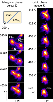
Fig. 3. Considered domain configurations (the top-left) and temperature dependence of the 2D speckle patterns of the BTO 200/002 reflections obtained from a BTO single grain. The left and right columns represent the pairs of 200T1/002T and 200T2/002T reflections for the tetragonal phase (T < TC), and the 200C reflection for the cubic phase (T > TC), respectively.
Download figure:
Standard image High-resolution imageA linear boundary and steep phase contrast are visible in the reconstructed images of a single BTO grain, despite the cubic phase. Figure 4(a) shows the 3D speckle pattern of the BTO single grain at 573 K; the red, yellow, and light blue colors indicate the order of intensity. The outer shape is reflected in the intense Bragg spots and streaks extending from the spots, whereas information on the atomic displacement from the average position is contained in the surrounding speckles. The 3D reconstructed image obtained by applying Bragg-CDI to a 3D speckle intensity of 200C [Fig. 4(a)] is shown in Fig. 4(b). The reconstructed image exhibits an outer shape with multiple planes, which are the grain boundaries caused by the sintering-induced grain growth. The image size is approximately 400 nm in the longitudinal direction, and the real-space resolution is approximately 13 nm. Figures 4(c) and 4(d) show the cross-sectional images of the amplitude (electron density distribution) and phase (lattice strain distribution), respectively, determined from the reconstructed structure factor. The images are cut by the blue plane parallel to Q . The electron density image exhibits a homogeneous distribution inside the outer shape, except at a few local density deficiencies (blue–green color). Only regions that satisfy the Bragg condition are reflected in the obtained CXD patterns and reconstructed images, because the electron density is equivalent to the norm components of the structural factors. The electron density deficiencies can be attributed to intracrystalline grain boundaries. The phase image shows the phase boundary along the direction indicated by the blue arrow at an angle of 45° from the Q vector. The linear region of the phase boundary is discontinued at the point where the electron density is low [dashed circles in Figs. 4(c) and 4(d)]. The phase contrast is approximately less than 0.4π near the phase boundary; this value corresponds to an atomic misalignment of 0.04 nm per 13 nm, because 2π corresponds to a (200) d-spacing of 0.2 nm. Figures 4(e) and 4(f) show the cross-sectional images of the electron density and lattice strain distribution cut by the blue plane approximately perpendicular to the Q vector. The electron density image displays the density-deficient regions with white arrows. Starting at the edges of these regions, the lattice strain image exhibits a steep contrast of more than π, corresponding to an atomic misalignment of more than 0.1 nm per 13 nm.
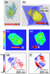
Fig. 4. (a) 3D speckle pattern and (b) reconstructed image of the 200C reflection from a BTO single grain at 573 K. Cross-sectional images of (b) cut by the plane parallel to Q [(c) the electronic density and (d) lattice strain distributions] and approximately perpendicular to Q [(e) the electronic density and (f) lattice strain distributions].
Download figure:
Standard image High-resolution imageThe CXD and Bragg-CDI results suggest that the BTO grains in the cubic phase inherit the boundaries of the 90° domains in the tetragonal phase and exhibit grain-boundary sliding. The pattern and boundary of the phase in Fig. 4(d) are consistent with the domain configuration and boundary of the tetragonal phase, respectively. To understand the structure of the tetragonal phase, we applied Bragg-CDI to the 200T1 and 002T reflections of a BTO single grain in the tetragonal phase at 313 K. Figure 5(a) shows the 3D speckle patterns corresponding to the 2D patterns at 313 K shown in Fig. 3 (viewed from different angles). We excluded the weaker reflection, i.e. 200T2 in Fig. 3, from this analysis, because although the domain corresponding to 200T2 and 002T forms another boundary elsewhere, the volume of the 200T2 domain is negligibly small. The 200T1 and 002T Bragg spots of BTO connected by the streak tail correspond to the adjacent 90° domains; 37) herein, 200T1 and 002T are named as the a- and c-domains, respectively. Figure 5(b) shows the reconstructed 3D outer shape of the BTO single grain consisting of a- and c-domains viewed from the same direction as that in Fig. 4(d). We obtained the reconstructed images with a real-space resolution of approximately 20 nm using the same procedure previously reported in Ref. 24. The outer shape, including the a- and c-domains, is consistent with that of the cubic phase [shown in Fig. 4(b)], whose outline is indicated by a dashed line. The reconstructed a- and c-domains exhibit a typical 90° domain boundary 38,39) represented by the perimeter of the area enclosed by a white hatched line in the direction indicated by the blue arrow. The domain boundary is oriented at an angle of 45° with respect to the Q vector and is perpendicular to the pair of Bragg spots, 200T1 and 002T. Although a detailed near-boundary structure is not available because of the inadequate spatial resolution, the spotted streak tail in the CXD pattern at 313 K suggests a domain wall of negligible width according to model calculations. 27,37) Notably, the domain boundary observed in the tetragonal phase [Fig. 5(b)] is at the same position as that of the phase boundary observed in the cubic phase [Fig. 4(d)]. In addition, the two regions with different phase values in the cubic phase are colored blue and red in Fig. 4(d), where the a- and c-domains exist prior to the structural phase transition. This domain configuration inheritance can be ascribed to the grain deformations caused by the stresses from the adjacent grains via the boundaries. The steep phase contrast in Fig. 4(f) suggests that grain-boundary sliding occurs at the two points indicated by the black arrows. The neighboring grains in polycrystalline materials have different shapes and faces in different directions. The various shapes, directions, and combinations result in sliding motion of the grains, and thus induce anisotropic deformations in the grains. Anisotropic deformation can retain the atomic misalignments where the domain boundary is located, even in the paraelectric phase. These results indicate that the misaligned structures in the paraelectric phase reflect the domain configurations in the ferroelectric phase, similar to a previous report. 27) In the present study, we did not identify any dislocation in the BTO grain. We rejected other possibilities for the origin of the phase contrast, increasing/decreasing lattice parameter, and lattice tilting; these deformations should have appeared as gradual phase changes; however, such a trend was not observed. Thus, the results indicate that the grain-boundary sliding deforms the grain anisotropically in the cubic phase, resulting in the 90° domain configuration of the grain.

Fig. 5. (a) 3D speckle pattern and (b) reconstructed image of the pair of 200T1/002T reflections from a BTO single grain at 313 K.
Download figure:
Standard image High-resolution image
The results obtained in this study explain the 200T-002T peak splitting in the speckle patterns recorded at 413–433 K, despite the cubic phase. As mentioned before and previously explained in size effect studies, 5,40) the BTO grains are subjected to an anisotropic lattice strain due to grain boundary effects, and hence, the apparent "TC" of a single grain may be higher than the intrinsic TC. Because not all grains are susceptible to similar stresses, the temperature at which the phase transition occurs may vary by 10 K for each grain.
4. Conclusions
We recorded the temperature dependence of the speckle pattern of a single-crystalline grain in a BTO polycrystalline ceramic using an MEMS heater and the CXD method, and investigated the structural changes in a 400 nm sized BTO single grain undergoing structural phase transition from the tetragonal to the cubic phase. One 200 Bragg spot in the cubic phase and a 200/002 Bragg spot pair with streak-tail scattering connecting the two spots in the tetragonal phase appeared. The reconstructed image showed a linear phase boundary, and a steep phase contrast began at the grain boundary. The CXD and Bragg-CDI results indicated that the BTO grain inherited domain configurations, even in the paraelectric phase, owing to grain-boundary sliding. Visualization of the submicrometer-sized structure using coherent X-rays significantly aided in understanding the external effects on the ferroelectricity and dielectric properties of ceramics.
Acknowledgments
We would like to thank Dr. J. R. Harries (QST) for discussions and comments. The compound refractive lenses used in the experiments were manufactured by the Karlsruhe Institute of Technology/Institute of Microstructure Technology and ASICON Tokyo Ltd. We also thank Nocada Inc. for providing the MEMS heating holder used in this study. This study was supported in part by a JSPS Grant-in-Aid for Scientific Research (Grant No. JP18H03850, JP18H05518, JP19H05819, JP19H05625, JP22H01976, JP23H01868, and JP23H04860); QST President's Strategic Grant (QST Advanced Study Laboratory); and QST Advanced Research Infrastructure for Materials and Nanotechnology under the remit of the "Advanced Research Infrastructure for Materials and Nanotechnology" of the Ministry of Education, Culture, Sports, Science and Technology (MEXT), Japan (Grant No. JPMXP1222QS0017). The synchrotron X-ray scattering experiments were performed at SPring-8 with the approval of JASRI (Proposal Nos. 2021A1100, 2021B1252, 2022A1172, 2022A3761, 2022A3762, 2022A3763, 2022A3784, 2022B1834, 2022B3761, 2022B3763, and 2022B3784).